 Zhou Dai
 Wei Li
 Chenxin Ma3
95% of researchers rate our articles as excellent or good
Learn more about the work of our research integrity team to safeguard the quality of each article we publish.
Find out more
ORIGINAL RESEARCH article
Front. Phys. , 30 May 2023
Sec. Interdisciplinary Physics
Volume 11 - 2023 | https://doi.org/10.3389/fphy.2023.1190073
This article is part of the Research Topic Advanced Signal Processing Techniques in Radiation Detection and Imaging View all 13 articles
This paper proposes a new design of an electromagnetic interference wideband filtering power divider (FPD) with a wide stopband based on the genetic algorithm (GA). A set of data structures is constructed by describing the corresponding connection method between the basic units and their electrical parameters in the three-port design. Then, the GA is used to find the appropriate design topology and electrical parameters, including isolation resistances, to meet FPD specifications by optimizing the data structures. For validation, one prototype is implemented. The results indicate that the new wideband FPD exhibits compact size, sharp roll-off, and good in-band isolations.
In recent years, with the rapid development of RF systems, there is an increasing demand for compact and high-performance RF equipment. The design of a highly integrated multifunctional microwave circuit can meet these needs well. Among them, a filtering power divider (FPD) with high performance, especially high isolation, becomes a research hotspot. For wideband (WB) application in wireless communication systems, WB-FPDs are desired and have been explored in [1–9]. A wideband FPD is introduced in [1], which sacrifices passband insertion loss. A wideband FPD with a wide stopband implemented by using open-stub loaded coupled lines [2, 3] presents a novel microstrip dual-mode FPD with a wide upper stopband. In [4–9], several FPDs are introduced, showing good performance in both the passband and stopband. However, the design of FPDs with merits of good insertion loss and high isolation still remains a great challenge.
On the other hand, in order to improve the design efficiency and performance of microwave circuits, multiple intelligent algorithms have been applied to the design [10–13]. [10] presented a computer-aided design procedure of the simulated annealing algorithm to optimize dual-wideband microstrip line filters. [11] proposed a novel method to model the microwave circuit by combining traditional full-wave electromagnetic simulation with the annealing algorithm for the first time. In [10], a compact dual-band bandpass filter was designed using the genetic algorithm (GA). Nevertheless, up to now, there are few algorithms used to design FPDs, not to mention wideband FPDs.
In this paper, a high-performance wideband FPD is designed using the GA. Taking advantage of the capability of avoiding the local optimal situation from the adaptive GA, suitable circuit topology, including the isolation network and corresponding electrical parameters, is determined to achieve the desired performance. To verify this design concept, a wideband FPD working at 1.3 GHz with a fractional bandwidth of 69.2% and out-of-band suppression greater than 4.5 times the center frequency is simulated, fabricated, and tested.
Since a three-port FPD can be considered a symmetrical structure, the even- and odd-mode analysis method can be applied. The equivalent odd- and even-mode circuits of the FPD can be obtained by setting the symmetrical plane open- and short-circuited ends, and the theoretical three-port scattering parameters can be easily obtained as follows:
where S11e and S11o denote reflection coefficients of the even- and odd-mode equivalent circuit models, respectively, while Se21 represents the transmission coefficients of the even-mode equivalent circuit model.
Traditionally, as shown in Figure 1A, any two-port microstrip circuit can be divided into basic circuit elements, as shown in Figure 1B. The circuit can be seen as a data structure, as shown in Figure 1C, composed of three sections. The first section is coded in integer which is determined by the topology of a basic element. The second section is coded in integer, which indicates the method of connection to the former elements. The third section coded in floating number and represents the corresponding electrical parameters. The details of the basic circuit elements are shown in Table 1. During the GA, a structure is chosen as a gene and a set of structures is set as a chromosome [14–16]. Therefore, it is obvious that the two-port even-mode equivalent circuit model of a microstrip FPD can be indicated by a chromosome.
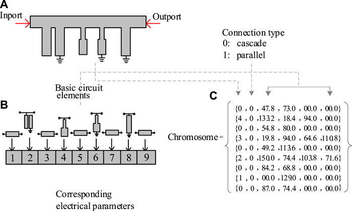
FIGURE 1. Representation scheme in the proposed algorithm. (A) Typical microstrip circuit working at 3.5 GHz. (B) Decomposition of the circuit in (A) into basic circuit elements. (C) Chromosome of the circuit in (A), a set of structures.
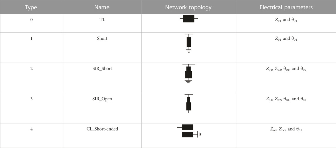
TABLE 1. Electrical parameters of the basic elements.
In this work, a wideband FPD is designed to improve the operation wideband performance and design efficiency by adopting the adaptive GA [17]. Different from the traditional GA, the adaptive GA changes the crossover and mutation probability with the fitness value automatically, which greatly increases the convergence accuracy and accelerates the convergence process of the GA. The optimization process is as follows: first, in the adaptive GA, the convergence time is influenced by the initial population significantly. Therefore, the corresponding electric length and characteristic impedance of each chromosome is randomly initialized between π/6–5π/6 and 20–150 Ω for practical implementation. Next, in order to effectively appraise the frequency response of chromosome [8], the transmission-line models are utilized to calculate the scattering parameter (S21e). Finally, the ABCD matrix chain of the chromosome is converted into a scattering matrix. The conversion process is shown in the following formula.
where Z01 and Z02 are the source and load impedances of the system, respectively, and R01 and R02 are the real parts of Z01 and Z02, respectively.
Then, the fitness value is designed as follows:
where N represents the number of sampling points, wi is the weighting value at the ith sampling parameter, and fi is the square deviation between the calculated scattering parameter (S21e) and the desired value at the ith sampling point.
Based on the ideal frequency response, the optimal solution is obtained by optimizing the topological structure and the corresponding electrical parameters. Here, in order to validate the proposed algorithm, a wideband FPD is designed and implemented. The specifications of the FPD are as follows:
Return losses within 0.5–2.0 GHz >20 dB.
Rejections within 2.0–6.0 GHz >20 dB.
Figure 2 shows the desired scattering parameters of the wideband FPD. The whole flowchart of the even-mode circuit optimization procedure for the desired power division filtering response is defined in the left part of Figure 4. In this design, the optimal chromosome after 45 generations is composed of four transmission lines, two short-ended stubs, and two coupled lines, which is used for the dual-port even-mode equivalent circuit model of the desired FPD. The final electrical parameters are shown in Table 2.

FIGURE 2. Desired function of the genetic algorithm.
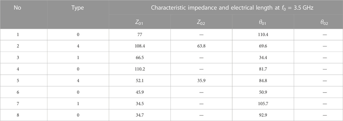
TABLE 2. Electrical and physical parameters of the initial FPD.
The next step is to obtain the isolation network configuration with high isolation performance. First, the positions of the isolation resistors need to be determined. In our design, when a short-ended stub or short-ended coupled line is introduced in each branch, a resistor will be placed between the connection points. Additionally, to simplify the configuration, a resistor is necessary when the next unit is a transmission line (TL) unit only. Therefore, three resistors are introduced, as shown in Figure 3C. On the other hand, to make the resistors achieve the satisfactory isolation performance, the resistances need to be set properly. These resistors are utilized in the GA as extended unknown design parameters of the genes, together with the known electrical parameters from the aforementioned determined even-mode equivalent circuit. The initial values of these resistors are set between 100 and 1,000 Ω. S23 is made to approach 0 to find the optimal resistances. More specifically, based on Eq. 1, it can be concluded that once the even-mode equivalent circuit is obtained, S23 is only affected by the odd-mode equivalent circuit. As a result, to obtain S23, the following equation should be optimized to approach 0:
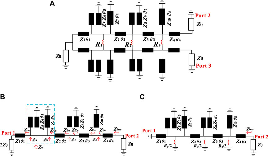
FIGURE 3. (A) Equivalent circuit of the proposed WB-FPD, (B) even mode, and (C) odd mode.
where
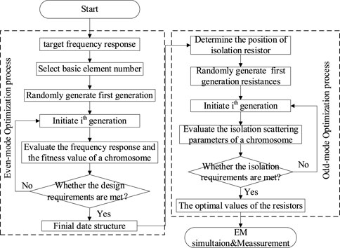
FIGURE 4. Flowchart of the proposed algorithm.
Based on the aforementioned design process, the final circuit structure is determined, as shown in Figure 3A. Figure 5 shows the theoretical filtering performance of the proposed WB-FPD circuit. It can be found that the design exhibits wideband and good spurious suppression, which meets the requirement well.
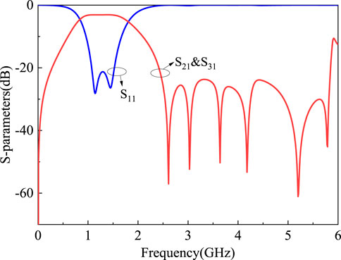
FIGURE 5. Theoretical filtering performance of the WB-FPD circuit.
In order to illustrate its high filtering performance better, the transmission zeros (TZs) will further be analyzed. Figure 3B shows the even-mode equivalent circuit, which can be utilized to obtain the filtering function. Herein, Zine is the input impedance, and it can be derived as follows:
where
Therefore, the reflection coefficient at output port 2 (or port 3) can be derived as follows:
Next, S21 can be determined as follows:
By setting |S21| = 0, six TZs are deduced as (9), which are generated by the short-ended stub and couple lines.
According to the aforementioned analysis, a WB-FPD prototype with f0 = 1.3 GHz is designed and manufactured. The proposed circuit is designed on a Rogers RO4003C substrate with a relative dielectric constant of 3.55, a loss tangent of 0.0027, and a thickness of h = 0.508 mm The corresponding parameters shown in Figure 3A are determined as follows (units: mm): L1 = 17.7, L2 = 12.53, L3 = 7.17, L4 = 12.79, L5 = 10.64, L6 = 35.07, L7 = 12.54, L8 = 15.72, W1 = 0.52, W2 = 0.21, W3 = 1.29, W4 = 2.18, W5 = 0.38, W6 = 0.68, W7 = 1.34, W8 = 0.76, S1 = 0.23, S2 = 0.11, and R1 = 100 Ω, R2 = 600 Ω, and R3 = 100 Ω. A photograph of the fabricated WB-FPD is shown in the inset of Figure 6A. The S-parameters are performed using the Agilent 5244 A network analyzer. As shown in Figures 6A,B, the measured center frequency is 1.3 GHz, and the corresponding 3-dB fractional bandwidth is 69.2%. The insertion loss in the passbands is 1.3 dB, while the return losses of the input and output are better than 20.3 and 22.4 dB, respectively. Six TZs can be found as expected, which help achieve good out-of-band suppression. In addition, the measured isolation is 19.8 dB within passbands.
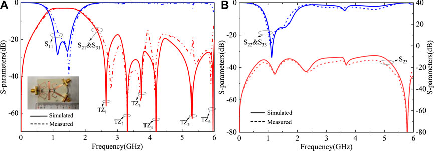
FIGURE 6. Measured and simulated results of the WB-FPD. (A) Magnitudes of S11, S21, and S31. (B) Magnitudes of S23, S22, and S33.
Table 3 shows a detailed comparison between the proposed design and other reported works. It can be concluded that this design can not only achieve wider working bandwidths and sharper frequency selectivity but also higher in-band isolation. It is also worth mentioning that it realizes a wideband FPD with a wide stopband design using the optimization algorithm for the first time.
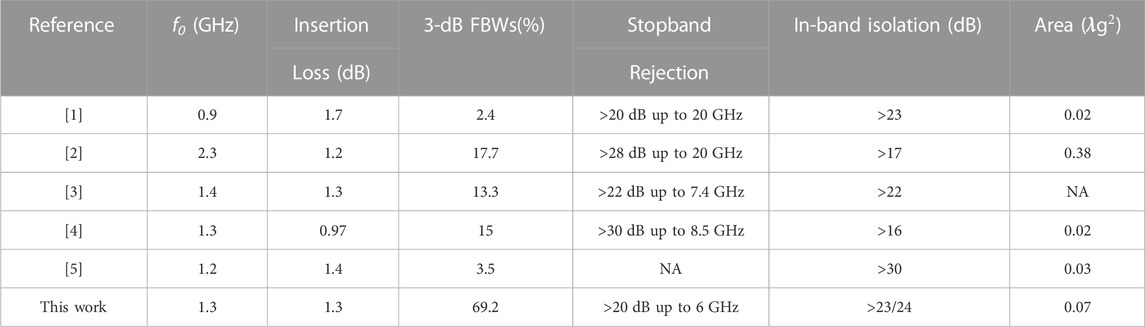
TABLE 3. Comparisons with other previous works.
In this paper, a new design of a wideband FPD with a wide stopband based on the GA is proposed. The analysis and design procedure have been illustrated. A prototype WB-FPD has demonstrated the design concept. With decent performance and high design efficiency, the proposal is attractive for wireless communication systems.
The original contributions presented in the study are included in the article/Supplementary Material; further inquiries can be directed to the corresponding authors.
ZD conducted extensive analysis and wrote parts of this paper. WL gave assistance in the measurement and wrote parts of this paper. CM, WZ, and WT wrote and revised this paper. All authors contributed to the article and approved the submitted version.
The authors declare that the research was conducted in the absence of any commercial or financial relationships that could be construed as a potential conflict of interest.
All claims expressed in this article are solely those of the authors and do not necessarily represent those of their affiliated organizations, or those of the publisher, the editors, and the reviewers. Any product that may be evaluated in this article, or claim that may be made by its manufacturer, is not guaranteed or endorsed by the publisher.
1. Chau W-M, Hsu K-W, Tu W-H. Filter-based Wilkinson power divider. IEEE Microw Wireless Compon Lett (2014) 24(4):239–41. doi:10.1109/lmwc.2014.2299543
2. Fan L, Qian HJ, Yangl B, Wang G, Luo X, "Filtering power divider with wide stopband using open-stub loaded coupled-line and hybrid microstrip T-stub/DGS cell," Proceedings of the 2018 IEEE/MTT-S International Microwave Symposium, Philadelphia, PA, USA, June 2018, pp. 1–4.
3. Zhang G, Wang J, Zhu L, Wu W. Dual-mode filtering power divider with high passband selectivity and wide upper stopband. IEEE Microw Wireless Compon Lett (2017) 27(7):642–4. doi:10.1109/lmwc.2017.2711556
4. Zhao X, Gao L, Zhang X, Xu J. Novel filtering power divider with wide stopband using discriminating coupling. IEEE Microw Wireless Compon Lett (2016) 26(8):580–2. doi:10.1109/lmwc.2016.2585551
5. Chen CF, Lin CY. Compact microstrip filtering power dividers with good in-band isolation performance. IEEE Microw Wireless Compon Lett (2014) 24(1):17–9. doi:10.1109/lmwc.2013.2287243
6. Gómez-García R, Loeches-Sánchez R, Psychogiou D, Peroulis D. Single/multi-band Wilkinson-type power dividers with embedded transversal filtering sections and application to channelized filters. IEEE Trans Circuits Syst Reg Pap (2015) 62(6):1518–27. doi:10.1109/tcsi.2015.2418838
7. Tian H, Dong Y. Packaged filtering power divider with high selectivity, extended stopband and wideband isolation. IEEE Trans Circuits Syst Exp Briefs (2023) 70(4):1311–5. doi:10.1109/tcsii.2022.3227169
8. Han C, Tang D, Deng Z, Qian HJ, Luo X. Filtering power divider with Ultrawide stopband and wideband low radiation loss using substrate integrated defected ground structure. IEEE Microw Wireless Compon Lett (2021) 31(2):113–6. doi:10.1109/lmwc.2020.3036419
9. Liu B -G, Lyu Y -P, Zhu L, Cheng C -H. Compact square substrate integrated waveguide filtering power divider with wideband isolation. IEEE Microw Wireless Compon Lett (2021) 31(2):109–12. doi:10.1109/lmwc.2020.3042332
10. Hsu MH, Huang JF. Annealing algorithm applied in optimum design of 2.4GHz and 5.2GHz dual-wideband microstrip line filters. IEICE Trans Elect (2005) E88C(1):47∼56.
11. Rayas-Sanchez JE. EM-Based optimization of microwave circuits using artificial neural networks: The state-of-the-art. IEEE Trans Microw Theor Techn. (2004) 52(1):420–35. doi:10.1109/tmtt.2003.820897
12. Pan Y, Dong J. Design and optimization of an ultrathin and broadband polarization-insensitive fractal FSS using the improved bacteria foraging optimization algorithm and curve fitting. Nanomaterials (2023) 13(1):191. doi:10.3390/nano13010191
13. Pan Y, Dong J, Wang M. Equivalent circuit-assisted multi-objective particle swarm optimization for accelerated reverse design of multi-layer frequency selective surface. Nanomaterials (2022) 12(21):3846. doi:10.3390/nano12213846
14. Lai M-I, Jeng S-K. Compact microstrip dual-band bandpass filters design using genetic-algorithm techniques. IEEE Trans Microw Theor Techn. (2006) 54(1):160–8. doi:10.1109/tmtt.2005.860327
15. Uhm M, Nam S, Kim J. Synthesis of resonator filters with arbitrary topology using hybrid method. IEEE Trans Microw Theor Tech. (2007) 55(10):2157–67. doi:10.1109/tmtt.2007.906505
16. Nicholson GL, Lancaster MJ. Coupling matrix synthesis of cross-coupled microwave filters using a hybrid optimisation algorithm. IET Microw Antennas Propag (2009) 3(6):950–8. doi:10.1049/iet-map.2008.0145
Keywords: filtering power divider (FPD), wideband, genetic algorithm (GA), wide stopband, isolation network
Citation: Dai Z, Li W, Ma C, Zhang W and Tang W (2023) Wideband electromagnetic interference filtering power divider with a wide stopband using the genetic algorithm. Front. Phys. 11:1190073. doi: 10.3389/fphy.2023.1190073
Received: 20 March 2023; Accepted: 10 May 2023;
Published: 30 May 2023.
Edited by:
Jian Dong, Central South University, ChinaReviewed by:
Guoan Wang, University of South Carolina, United StatesCopyright © 2023 Dai, Li, Ma, Zhang and Tang. This is an open-access article distributed under the terms of the Creative Commons Attribution License (CC BY). The use, distribution or reproduction in other forums is permitted, provided the original author(s) and the copyright owner(s) are credited and that the original publication in this journal is cited, in accordance with accepted academic practice. No use, distribution or reproduction is permitted which does not comply with these terms.
*Correspondence: Zhou Dai, ZGFpemhvdTE5ODZAMTYzLmNvbQ==; Wei Li, bGl3ZWlfbm51QDE2My5jb20=
Disclaimer: All claims expressed in this article are solely those of the authors and do not necessarily represent those of their affiliated organizations, or those of the publisher, the editors and the reviewers. Any product that may be evaluated in this article or claim that may be made by its manufacturer is not guaranteed or endorsed by the publisher.
Research integrity at Frontiers
Learn more about the work of our research integrity team to safeguard the quality of each article we publish.