 Chenyu Yao
 Mengjie Jiang1
 Lin Wang
- 1State Key Laboratory for Infrared Physics, Shanghai Institute of Technical Physics, Chinese Academy of Sciences, Shanghai, China
- 2University of Chinese Academy of Sciences, Beijing, China
- 3College of Physics and Optoelectronic Engineering, Hangzhou Institute for Advanced Study, University of Chinese Academy of Sciences, Hangzhou, China
- 4Zhejiang Lab, Intelligent Perception Research Institute, Research Center for Quantum Sensing, Hangzhou, China
Terahertz (THz) detection has been extensively studied in the application fields of wireless communication, non-destructive imaging and spectrum inspection, etc., in the decades. Here, we report that a self-mixing terahertz detector based on hemispherical silicon lens and antenna-coupled InGaAs/AlGaAs high electron mobility transistor (HEMT) enables wide spectrum detection, and improves detection performances. In this device configuration, the optimal log-periodic antenna is used to enhance light field in the channel, the double-gate could further adjust the carrier concentration, and the hemispheric silicon lens can concentrate the terahertz radiation in the center of the hemisphere to effectively improve the terahertz wave collection efficiency, which could improve the sensitivity of the detector. The broadband Terahertz responsivity and noise equivalent power (NEP) of the detector are characterized at the range from 0.07 to 0.82 THz at room temperature. A peak responsivity of 2 kV/W and a minimum optical noise equivalent power of 59 pW/Hz1/2 at 0.8 THz without any external field, are reached from two-terminal configuration at 0.8 THz. The minimum optical NEP of the device can be reduced to 30 pW/Hz1/2 by applying a gate voltage, realizing scanning imaging demonstration.
Introduction
Terahertz radiation (0.1–10 THz) is characterized by its high frequency, ultrashort pulse duration (in the picosecond range), low photon energy, and strong penetrating power. These remarkable properties make it a highly promising technology for various applications, including material research, safety inspection, environmental monitoring, and communication [1–3]. The primary approach to harnessing terahertz radiation is via terahertz detection technology, which significantly impacts both fundamental and applied terahertz research. One of the foundational tools for advancing terahertz application technology and a key method and primary component of terahertz scientific study is the development of room temperature, high-speed, and high-sensitivity terahertz wave detectors. Detectors based on thermal detection principles, such as Golay cells, pyroelectric detectors, and bolometers, have gained widespread use [4]. However, such devices have limitations including low modulation speed, relatively large area, and reliance on external filters, which severely restrict their practicality. On the other hand, a type of uncooled THz detector that includes Schottky barrier detectors [5, 6] and families of detectors based on field-effect transistors (FETs), offer high appeal due to their fast response time and high sensitivity. Additionally, FET-based detectors have greatly benefited from advances in integrated circuit technology, allowing for the creation of large arrays [7–11].
The High Electron Mobility Transistor (HEMT) is a type of field-effect transistor that utilizes a heterojunction structure, also known as a modulation-doped field-effect transistor or a two-dimensional electron gas (2DEG) field-effect transistor. The device uses two materials with different energy gaps to create a heterojunction, resulting in the generation of a triangular potential well at the interface. The 2DEG within this potential well functions as the channel for field-effect transistor regulation. The unique spatial isolation of electrons and holes within the heterostructure’s potential well enables high electron mobility, which is responsible for the device’s outstanding properties, including large transconductance, low noise, high cut-off frequency, and fast switching speed. These characteristics make the HEMT an ideal choice for microwave amplifiers and power devices, and its potential for future applications is significant [12–15]. The cut-off frequency formula of HEMT shows that the highest can only be more than 100 GHz. When the terahertz wave of (0.1–10 THz) is irradiated, it is difficult to generate a photoelectric response, and it is difficult to directly detect the terahertz wave [16, 17]. Dyakonov and Shur proposed for the first time that the detection of terahertz waves could be realized by using the nonlinearity of plasma [18, 19]. Plasma waves belong to a form of periodic collective motion of electrons. In the past 10 years, many groups have successively realized room-temperature field-effect terahertz detectors based on CMOS, III-V compound semiconductors and graphene [20–27]. Using the AlGaAs/GaAs HEMT tri-gate device successfully realized the spectrum detection from 185 to 380 GHz, and successfully distinguished the high-order plasma mode, and the responsivity and noise equivalent power (NEP) at 11.5 K reached 100 kV/W and 50 pW/Hz1/2 respectively [28]. A GaN/AlGaN HEMT based on a special butterfly antenna coupling achieves a NEP value of 21 pW/Hz1/2 at 0.52 THz [27].
Simple field-effect transistor terahertz detectors have low responsivity and high equivalent noise power, so it is necessary to integrate some special structures in the transistor structure, such as grating-gate, planar antenna, etc. Among them, the planar antenna is convenient and has high coupling efficiency, which can greatly improve the performance of the detector, so it has attracted the attention of many scholars. Planar dipole antennas have various structures, including bowtie antennas, helical antennas, log-periodic antennas, and slot antennas. The integration of a butterfly antenna with a GaN/AlGaN HEMT structure, featuring a gate length of 0.25 μm, has been demonstrated to achieve outstanding performance with a NEP as low as 0.125 nW/Hz1/2 [22]. Meanwhile, the helical antenna, a type of circularly polarized antenna, is well-suited for applications where the polarization direction is uncertain or changing over time. By utilizing this antenna, a graphene terahertz detector has been able to achieve an impressive responsivity of 28 V/W [29]. Additionally, the log-periodic antenna is characterized by its broad bandwidth and numerous resonant peaks. In 2010, Dyer successfully integrated a high-bandwidth log-periodic antenna with a GaAs/AlGaAs HEMT, enabling the resonance detection of a terahertz detector at 20 K within the 0.235–0.24 THz frequency range [30]. Designing materials and structures for higher frequency terahertz detection requires careful consideration. InP-based HEMTs can achieve an electron mobility of 11,000 cm2/(V·s), and when combined with a nanoscale grating structure, a maximum response of more than 20 kV/W can be achieved at 200 and 292 GHz. Meanwhile, an ultra-low NEP of 0.48 pW·Hz−1/2 is obtained at 200 GHz [31]. However, this impressive NEP relies on high-quality material growth and high-precision device fabrication processes, which is both its strength and a limiting factor for its widespread adoption. Due to the long wavelength of terahertz radiation, it is challenging to focus the beam on the core region of the terahertz antenna due to the limit of optical diffraction. As a result, the detector’s effective light receiving area is limited, which makes detecting most terahertz waves difficult, leading to poor optical sensitivity. This presents a severe constraint for field-effect detectors, necessitating the development of a compact, high-speed, high-sensitivity, high-stability, and portable terahertz detector module. To address this, a commonly used quasi-optical focusing element in the terahertz band is a hemispherical silicon lens. This lens effectively increases the terahertz electric field strength and reduces the terahertz spot size, which helps to irradiate the detector surface with more terahertz waves, thereby improving the detector’s responsivity [32, 33]. Silicon lenses have been used to improve the performance of terahertz detectors before, enabling passive detection of 10 GHz–2.52 THz at room temperature [34]. Furthermore, coordinating the silicon lens and substrate can minimize substrate interference, expanding the detector’s response frequency band and increasing its consistency.
In this letter, we present a GaAs HEMT epitaxial wafer with a specific structure and a monolithic detector chip featuring a dual-grid logarithmic antenna structure. To enhance the gain, we employ a hemispherical silicon lens, which was also simulated. Notably, the silicon lens can amplify the terahertz wave electric field’s focus at the center by up to 4.5 times. The module, integrated into the silicon lens package, achieves wide-band detection of 0.07–0.82 THz, with a responsivity of 2 kV/W and a NEP of 59 pW·Hz−1/2 at a high frequency of 0.8 THz. We further improved the detector performance by applying a gate voltage to the channel, reducing the NEP to 30 pW·Hz−1/2. Additionally, we conducted terahertz imaging experiments with the unit module and obtained high-frequency terahertz images. Our work has significant implications for exploring HEMT integrated modules’ application in the terahertz field.
Simulation and design
Figures 1A, B depicts the structure of the proposed detector. The detector is mainly composed of high-resistance silicon lens, GaAs HEMT antenna chip and readout circuit. All components are assembled in a metal shielded box, leaving space outside the lens, and three SMA port connectors. The dielectric lens is held by the retaining ring, and the antenna chip is placed directly on the back of the lens as the main source. Based on the above design, the terahertz radiation from space is focused by the lens and received by the on-chip antenna in a back-illuminated manner. Supplementary Figure S1 shows a schematic diagram of our material structure (refer to the method for the specific structure), the two-dimensional electron gas concentration Ns = 2.4 × 10¹²/cm2 of our material.
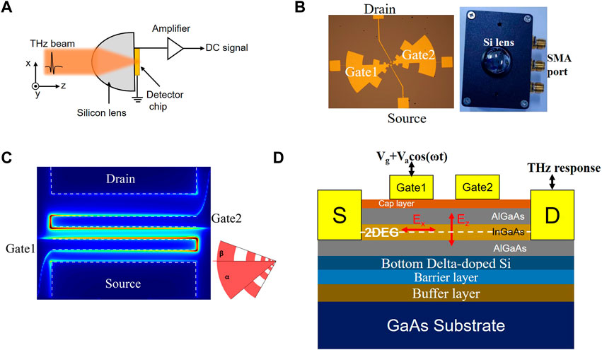
FIGURE 1. Module structure. (A) Silicon lens model design. (B) Component physical diagram and antenna structure diagram. (C) Antenna simulation result plot. Inset: Schematic diagram of the simulation parameters. (D) Schematic diagram of self-mixing detection.
We use time-domain numerical simulation technology to design a sub-wavelength coupling structure suitable for field effects, and realize a field effect integrated structure with broadband detection function by improving the existing antenna structure. The logarithmic periodic antenna is a well-established antenna structure that boasts an exceptionally broad operating bandwidth, capable of reaching 10:1 or wider [27, 28, 33, 34]. The dimensions of the oscillators of the log-periodic antenna designed in this paper satisfy the relationship:
Here, Rn represents the vertical distance from the geometric vertex of the antenna to the nth oscillator, where the oscillator is assigned a serial number of n. The logarithmic periodic antenna emits electromagnetic waves that are linearly polarized, with the polarization direction aligned parallel to the direction of the vibrator. It consists of a double-grid logarithmic periodical antenna with left and right lobes and a symmetrical source-drain antenna. Its resonant frequency is closely related to the length and angle of the lobes. The angle is determined as α = 45°, β = 30°.
The terahertz response of our device is a result of the combined impact of the photo-thermoelectric effect and self-mixing mechanism, which are contingent upon the specific working states of the device. When there is no external bias voltage (no gate voltage), the device works under the photo-thermoelectric mechanism. The asymmetric light field shown in Figure 1C. Hot carrier diffusion produces a temperature gradient, which drives the directional movement of carriers to generate photocurrent [27]. As depicted in Figures 2B–E, our device exhibits a favorable response even in the absence of a gate voltage.
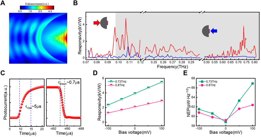
FIGURE 2. Device performance characterization. (A) Silicon lens simulation results. (B) Device response spectrum. (C) Device response time. (D) Curves of responsivity versus bias voltage at 0.73 and 0.8 THz. (E) NEP curves for bias voltages at frequencies of 0.73 and 0.8 THz.
When the device is subjected to both gate voltage and source-drain voltage, it operates based on the principle of plasma wave terahertz detection. The non-linear characteristics of plasma waves can detect terahertz waves. It was first proposed by Dyakonov and Shur that terahertz waves excite plasma waves in the channel [18, 19]. The nonlinear characteristics of plasma waves and asymmetric boundary conditions can induce a constant voltage is the terahertz response. With the deepening of research, a theoretical model of frequency mixing detection has recently been proposed [23–26]. Gated terahertz frequency mixing detector is composed of a high electron mobility transistor integrated with a terahertz antenna. The terahertz wave, denoted by ωTHz, is coupled into the channel of a two-dimensional electron gas, which is controlled by a field effect gate, through a terahertz antenna. The lateral terahertz electric field then modulates the drift velocity of the electrons in the two-dimensional electron gas channel, resulting in a modulation of
E0 is the free space terahertz electric field intensity; Z0 (
Utilizing finite difference time domain (FDTD) simulation, it is evident that the silicon lens exhibits a robust aggregating and enhancing effect on the electric field of the terahertz wave, as illustrated in Figure 2A. The diameter of the silicon lens is 10 mm, and to achieve the optimal terahertz light focusing effect, the GaAs substrate of the terahertz detector chip was thinned to 200 μm. Under the influence of the silicon lens, the terahertz wave is focused to a region of nearly 100 microns in the core of the lens. Although there is an impedance mismatch between the permittivity of the terahertz silicon lens and free space, about 30% of the terahertz wave is reflected, but at a frequency of 0.8 THz, the terahertz electric field in the center area of the silicon lens increases by 4.5 times compared to the incident terahertz wave, as seen in Figure 2A. Considering that the energy density of the electric field is proportional to the square of its intensity, the energy density within the core area of the detector can be increased up to approximately 20 times that of the incident terahertz wave due to the near-field convergence of the silicon lens. This enhancement in energy density has significant potential to boost the detector’s responsivity.
Test results
Figure 2B depicts the responsivity of the terahertz module detector integrated with the silicon lens. The photoresponse at zero source-drain voltage originates from the photo-thermoelectric effect, which benefits from our designed asymmetric structure. To assess the light-gathering efficiency of the lens, we carried out terahertz response tests on the detector module under front and back illumination, as illustrated in Figure 2B. The blue solid line in the figure corresponds to back illumination, which is equivalent to direct incidence of the terahertz wave on the detector chip surface. The red solid line in the figure represents front illumination, where the terahertz wave is focused onto the chip surface through the silicon lens. As a result of the amplified terahertz electric field, the terahertz response rate increases by about 20 times, which is consistent with the simulation results in Figure 2A. The frequency band of the incident terahertz wave is 0.02–0.82 THz. The device response time is shown in Figure 2C, with the turn-on time being about 5 μs and the turn-off time being around 0.7 μs. These results demonstrate the high-speed nature of our devices, making them ideal for applications in high-speed communications. We measured the source-drain voltage dependence curve of the module under 0.73 and 0.8 THz light as shown in Figure 2D. NEP, which measures the responsivity of photodetection, is calculated by taking the ratio of noise voltage density and responsivity (Vn/R). The noise spectral density reflects various noise sources present in the system, including but not limited to 1/f noise, shot noise, and Johnson-Nyquist noise. Supplementary Figure S2A is the noise spectrum of the test of the detector module. According to the noise spectrum, we calculated the NEP test results of the device, as shown in Figure 2E. Under zero bias voltage, the minimum NEP value of the module device can reach 59 pW/Hz1/2. Our four-end antenna structure is capable of efficiently coupling terahertz optical fields, but there is still room for improvement. We anticipate that even better results can be achieved by constructing the gate electrode with nanometer precision and incorporating a grating structure [31].
The source-drain current in a field effect transistor (FET) is influenced by both the source-drain voltage and the gate voltage. The correlation between the fixed gate voltage, source-drain voltage, and source-drain current is referred to as the output characteristic curve. Likewise, the transfer characteristic curve is used to describe the relationship between gate voltage and source-drain current at a fixed source-drain voltage. In our work, Gate1 plays the role of gate voltage regulation, and Gate2 only serves as antenna coupling. Figure 3A depicts the saturation characteristics of a HEMT. At a specific gate voltage, the source-drain current increases linearly with increasing source-drain voltage until saturation occurs, which is characterized by the saturation voltage Vdsat. Once the transistor reaches this point, it enters the saturation region where the source-drain current no longer increases linearly with increasing source-drain voltage. Moreover, as the gate voltage decreases, the saturation voltage also decreases. The transfer characteristic curve of HEMT, which provides information on the transistor’s threshold value, is shown in Figure 3B. The measurement curve in Supplementary Figure S3 represents the relationship between channel conductance and gate voltage when the source-drain voltage is held constant at 0.1 V. Additionally, Figures 3C, D illustrate the gate-controlled photoresponse curves under 0.73 and 0.8 THz terahertz wave illumination, respectively. The module’s maximum responsivity occurs when the gate voltage is approximately 0.6 V. Furthermore, Supplementary Figure S2B shows the noise equivalent power (NEP) curve of the device with respect to the gate voltage, with the module device reaching an NEP of 30 pW·Hz−1/2 at a gate voltage of 0.6 V. To demonstrate the effectiveness of our method, we complete a table (Table 1) and compare key parameters such as responsivity, NEP and response band between our detector and other detectors. At least one specification of our device is stronger than that of a reported work. Due to equipment limitations, we measured the responsivity and NEP profiles of the chip (without lens) at both room temperature and low temperature. We found that the responsivity and NEP of the unpackaged device were better at low temperatures due to lower thermal noise and larger mobility. This data has been included in Supplementary Figures S4A, B.
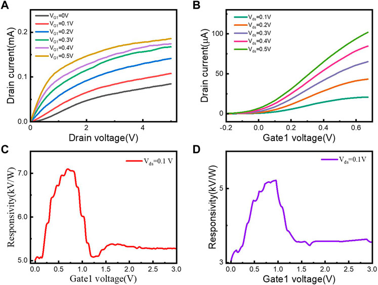
FIGURE 3. Characteristic curves under module gating control. (A) The output characteristic curve of device. (Under different gate1 bias) (B) The transfer characteristic curve of device. (Under different source-drain bias) (C) Gating control response curve at 0.73 THz. (D) Gating control response curve at 0.8 THz.
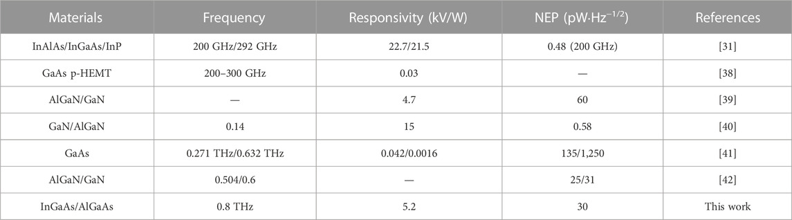
TABLE 1. Comparison of key parameters.
Terahertz imaging is a critical research area, and our module device demonstrates high responsivity and stable response output, making it an ideal choice for exploring terahertz scanning imaging applications. We have developed an optical system, as illustrated in Figure 4A, where a motor-controlled imaging object is scanned point by point, and the detector module signal at 0.8 THz is captured by a computer via an amplifier. The collected signal is subsequently processed by programming software to generate an image, as shown in Figure 4B. The resulting projection imaging data highlights intricate details, including the key outline and the structure of the metal triangle. Notably, even when an object is enclosed and visually undetectable, our detector module can scan every detail of the target object.
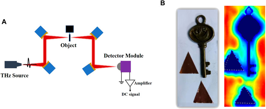
FIGURE 4. Modular imaging application. (A) Optical path diagram of terahertz imaging system. (B) Imaged objects and imaging results.
Discussion
In this study, we presents a novel high-sensitivity broadband room temperature terahertz module detector that integrates a hemispherical silicon lens. The detector utilizes a GaAs high electron mobility transistor with a unique structure. The joint coupling effect of the silicon lens and the four-terminal antenna improves the optical sensitivity of the detector; in addition, the back-illuminated method can eliminate the interference effect of the device substrate and improve the response bandwidth. At room temperature, the module detector achieves a wide-spectrum response of 0.07–0.82 THz, of which the responsivity at 0.73 and 0.8 THz are 4 and 2 kV/W, respectively, and the corresponding NEPs are 59 pW/Hz1/2 and 60 pW/Hz1/2, respectively. To enhance the module device’s performance, we implemented gate voltage regulation, resulting in a reduction of the NEP to 30 pW/Hz1/2 with a gate voltage regulation of 0.6 V. Finally, based on this module detector, the terahertz imaging application at a high frequency of 0.8 THz is realized. Our detector module has the characteristics of miniaturization, portability, room temperature operation and high sensitivity, and can be applied in terahertz-related fields.
Methods
Materials structure
On the GaAs substrate, grow 200 nm GaAs buffer layer, 250 nm AlxGa1-xAs buffer layer, 20 nm AlxGa1-xAs barrier layer, Si delta-doped bottom layer, 6 nm AlxGa1-xAs spacer layer, 10 nm InxGa1-xAs channel layer, 6 nm AlxGa1-xAs spacer layer, Si delta-doped layer, 22 nm AlxGa1-xAs barrier layer, 2 nm undoped AlAs layer, 15 nm undoped GaAs layer, 1.5 nm Si-doped AlAs barrier layer and 25 nm Si-doped GaAs cap layer. The source and the drain are respectively in contact with the GaAs buffer layer and both ends of each barrier layer to form ohmic contacts, and a (2-DEG) channel is formed between the channel layers.
Device fabrication process
The material grown by the MBE method was ultrasonically cleaned in acetone, isopropanol and deionized water for 5 min respectively. Use the method of ultraviolet lithography (MA6) to photoetch the channel, and then etch it by wet etching method. The etching depth is 110–130 nm, the etching time is about 28 s, and the composition ratio of the etching solution is H3PO4: H2O2: H2O = 1:1:25. The corroded samples were cleaned again in the above-mentioned manner. The source and drain ends of the device were etched out again using MA6, and then a metal layer of AuGe/Ni/Au = 100/20/300 nm was evaporated by electron beam evaporation (EBE-07). Then the excess metal was stripped off, annealed in a rapid annealing furnace, maintained at 450°C for 30 s, and the annealing was completed. Then perform an IV test on both ends of the device to confirm that the ohmic contact of the device is good. Finally, the gate electrode is etched out by ultraviolet lithography (MA6), and a metal layer of Ti/Au = 30/100 nm is deposited by electron beam evaporation (EBE-07), and a Schottky contact is formed after the lift-off process.
Photocurrent measurements
The electrical characteristics of the devices were measured using a Semiconductor Parameter Analyzer (B2912A). To obtain light response data, a custom optical setup was used. The setup involved using continuous low-energy photons that were modulated by the electric chopper of a microwave source (Agilent E8257D). These photons passed through a frequency doubler (VDI WR 9.0) and a lock-in amplifier (SR830) to obtain a detection current of 0.1 THz. Additionally, the 0.3 THz radiation was generated by a 0.1 THz IM PATT diode that was connected to a VDI WR 2.8 tripler. Use a low-frequency microwave generator (WA-04609) to generate low-frequency microwaves to generate 0.49–0.82 THz electromagnetic waves through a multiplying link (VDI WR 1.9). To enable the locking procedure in the presence of DC offset and 1/f noise, the amplitude of the terahertz wave was electronically chopped using a 1 kHz square wave signal. This ensured that the terahertz wave was TTL modulated. The power density of the terahertz waves was measured using a commercially calibrated photoconductive terahertz power meter (TK100). The responsivity RV is extracted from the measured Iph as RV = Iph∙r/(P∙S), where P is the power density, S is the effective area S = λ2/4π, and r is the device resistance. All measurements were performed under room temperature ambient conditions.
Data availability statement
The original contributions presented in the study are included in the article/Supplementary Material, further inquiries can be directed to the corresponding authors.
Author contributions
All authors listed have made a substantial, direct, and intellectual contribution to the work and approved it for publication.
Funding
This work was supported in part by the National Key R&D Program of China (No. 2021YFB2800702), Fundamental Research Funds for the Central Universities (2232022A-11), Zhejiang Lab (No. 2021MB0AB01), Shanghai Natural Science Foundation Project (21ZR1402200, 21ZR1473800).
Conflict of interest
The authors declare that the research was conducted in the absence of any commercial or financial relationships that could be construed as a potential conflict of interest.
Publisher’s note
All claims expressed in this article are solely those of the authors and do not necessarily represent those of their affiliated organizations, or those of the publisher, the editors and the reviewers. Any product that may be evaluated in this article, or claim that may be made by its manufacturer, is not guaranteed or endorsed by the publisher.
Supplementary material
The Supplementary Material for this article can be found online at: https://www.frontiersin.org/articles/10.3389/fphy.2023.1182059/full#supplementary-material
References
1. Rogalski A, Sizov F. Terahertz detectors and focal plane arrays[J]. Opto-electronics Rev (2011) 19(3):346–404.
2. Nagatsuma T, Ducournau G, Renaud CC. Advances in terahertz communications accelerated by photonics. Nat Photon (2016) 10(6):371–9. doi:10.1038/nphoton.2016.65
3. Naftaly M, Vieweg N, Deninger A. Industrial applications of terahertz sensing: State of play. Sensors (2019) 19(19):4203. doi:10.3390/s19194203
4. Khanna VK. Bolometers, Golay cells and pyroelectric detectors[M]. In: Practical Terahertz Electronics: Devices and Applications, Volume 2: Optical devices and applications. IOP Publishing (2021).
5. Shin JH, Park DW, Lee ES, Kim M, Lee IM, et al. Highly reliable THz hermetic detector based on InGaAs/InP Schottky barrier diode. Infrared Phys Tech (2021) 115:103736. doi:10.1016/j.infrared.2021.103736
6. Sai P, But DB, Yahniuk I, Grabowski M, Sakowicz M, Kruszewski P, et al. AlGaN/GaN field effect transistor with two lateral Schottky barrier gates towards resonant detection in sub-mm range. Semiconductor Sci Tech (2019) 34(2):024002. doi:10.1088/1361-6641/aaf4a7
7. Al Hadi R, Sherry H, Grzyb J, Zhao Y, Forster W, Keller HM, et al. A 1 k-pixel video camera for 0.7-1.1 terahertz imaging applications in 65-nm CMOS. IEEE J Solid-state Circuits (2012) 47:2999–3012. doi:10.1109/jssc.2012.2217851
8. Lisauskas A, Bauer M, Boppel S, Mundt M, Khamaisi B, Socher E, et al. Exploration of terahertz imaging with silicon MOSFETs. J Infrared, Millimeter, Terahertz Waves (2014) 35:63–80. doi:10.1007/s10762-013-0047-7
9. Boukhayma A, Dupret A, Rostaing JP, Enz C. A low-noise CMOS THz imager based on source modulation and an in-pixel high-Q passive switched-capacitor N-path filter. Sensors (2016) 16(3):325. doi:10.3390/s16030325
10. Zdanevičius J, Bauer M, Boppel S, Palenskis V, Lisauskas A, Krozer V, et al. Camera for high-speed THz imaging. J Infrared, Millimeter, Terahertz Waves (2015) 36:986–97. doi:10.1007/s10762-015-0169-1
11. Yokoyama S, Ikebe M, Kanazawa Y. 5.8 A 32× 32-pixel 0.9 THz imager with pixel-parallel 12b VCO-based adc in 0.18 μm CMOS[C]. In: 2019 IEEE International Solid-State Circuits Conference-(ISSCC). IEEE (2019). p. 108–10.
12. Mimura T. The early history of the high electron mobility transistor (HEMT). IEEE Trans Microwave Theor Tech (2002) 50(3):780–2. doi:10.1109/22.989961
13. He J, Cheng WC, Wang Q, Cheng K, Yu H, Chai Y. Recent advances in GaN-based power HEMT devices. Adv Electron Mater (2021) 7(4):2001045. doi:10.1002/aelm.202001045
14. Satou A, Otsuji T. Recent progress in the development of grating-gate InGaAs-channel HEMTs for fast and sensitive THz detection[J]. Terahertz Emitters, Receivers, Appl XIII (2022) 12230:80–5.
15. Tamura K, Tang C, Ogiura D, Suwa K, Fukidome H, Takida Y, et al. Fast and sensitive terahertz detection with a current-driven epitaxial-graphene asymmetric dual-grating-gate field-effect transistor structure. APL Photon (2022) 7(12):126101. doi:10.1063/5.0122305
16. Lin YM, Dimitrakopoulos C, Jenkins KA, Farmer DB, Chiu HY, Grill A, et al. 100-GHz transistors from wafer-scale epitaxial graphene. Science (2010) 327(5966):662. doi:10.1126/science.1184289
17. Wu Y, Lin Y, Bol AA, Jenkins KA, Xia F, Farmer DB, et al. High-frequency, scaled graphene transistors on diamond-like carbon. Nature (2011) 472(7341):74–8. doi:10.1038/nature09979
18. Dyakonov M, Shur M. Detection, mixing, and frequency multiplication of terahertz radiation by two-dimensional electronic fluid. IEEE Trans Electron Devices (1996) 43(3):380–7. doi:10.1109/16.485650
19. Dyakonov M, Shur M. Shallow water analogy for a ballistic field effect transistor: New mechanism of plasma wave generation by dc current. Phys Rev Lett (1993) 71(15):2465–8. doi:10.1103/physrevlett.71.2465
20. Javadi E, But DB, Ikamas K, Zdanevičius J, Knap W, Lisauskas A. Sensitivity of field-effect transistor-based terahertz detectors. Sensors (2021) 21(9):2909. doi:10.3390/s21092909
21. Vicarelli L, Vitiello MS, Coquillat D, Lombardo A, Ferrari AC, Knap W, et al. Graphene field-effect transistors as room-temperature terahertz detectors. Nat Mater (2012) 11(10):865–71. doi:10.1038/nmat3417
22. Bauer M, Lisauskas A, Boppel S. Bow-tie-antenna-coupled terahertz detectors using AlGaN/GaN field-effect transistors with 0.25 micrometer gate length[C]. In: 2013 European Microwave Integrated Circuit Conference. IEEE (2013). p. 212–5.
23. Sun JD, Sun YF, Wu DM, et al. High-responsivity, low-noise, room-temperature, self-mixing terahertz detector realized using floating antennas on a GaN-based field-effect transistor[J]. Appl Phys Lett (2012) 100(1):013506.
24. Sun YF, Sun JD, Zhou Y, Tan RB, Zeng CH, Xue W, et al. Room temperature GaN/AlGaN self-mixing terahertz detector enhanced by resonant antennas. Appl Phys Lett (2011) 98(25):252103. doi:10.1063/1.3601489
25. Sun J, Zhu Y, Feng W, Ding Q, Qin H, Sun Y, et al. Passive terahertz imaging detectors based on antenna-coupled high-electron-mobility transistors. Opt Express (2020) 28(4):4911–20. doi:10.1364/oe.385042
26. Sun JD, Qin H, Lewis RA, et al. Probing and modelling the localized self-mixing in a GaN/AlGaN field-effect terahertz detector. Appl Phys Lett (2012) 100(17):173513. doi:10.1063/1.4705306
27. Amirmazlaghani M, Raissi F. Feasibility of room-temperature GHz-THz direct detection in graphene through hot-carrier effect. IEEE Trans Device Mater Reliability (2018) 18(3):429–37. doi:10.1109/tdmr.2018.2862642
28. Dyer GC, Preu S, Aizin GR, Mikalopas J, Grine AD, Reno JL, et al. Enhanced performance of resonant sub-terahertz detection in a plasmonic cavity. Appl Phys Lett (2012) 100(8):083506. doi:10.1063/1.3687698
29. Guo W, Wang L, Chen X, Liu C, Tang W, Guo C, et al. Graphene-based broadband terahertz detector integrated with a square-spiral antenna. Opt Lett (2018) 43(8):1647–50. doi:10.1364/ol.43.001647
30. Dyer GC, Vinh NQ, Allen SJ, Aizin GR, Mikalopas J, Reno JL, et al. A terahertz plasmon cavity detector. Appl Phys Lett (2010) 97(19):193507. doi:10.1063/1.3513339
31. Kurita Y, Ducournau G, Coquillat D, Satou A, Kobayashi K, Boubanga Tombet S, et al. Ultrahigh sensitive sub-terahertz detection by InP-based asymmetric dual-grating-gate high-electron-mobility transistors and their broadband characteristics. Appl Phys Lett (2014) 104(25):251114. doi:10.1063/1.4885499
32. Sherry H, Al Hadi R, Grzyb J. Lens-integrated THz imaging arrays in 65nm CMOS technologies[C]. In: IEEE Radio Frequency Integrated Circuits Symposium. IEEE (2011). p. 1–4.
33. Jalili H, Momeni O. A 0.46-THz 25-element scalable and wideband radiator array with optimized lens integration in 65-nm CMOS. IEEE J Solid-State Circuits (2020) 55(9):2387–400. doi:10.1109/jssc.2020.2989897
34. Seliuta D, Kasalynas I, Tamosiunas V, et al. Silicon lens-coupled bow-tie InGaAs-based broadband terahertz sensor operating at room temperature[J]. Electron Lett (2006) 42(14):1.
35. Mistry KK, Lazaridis PI, Zaharis ZD, Loh TH. Design and optimization of compact printed log-periodic dipole array antennas with extended low-frequency response. Electronics (2021) 10(17):2044. doi:10.3390/electronics10172044
36. Rasheed FM, Abdulnabi HA. Toothed log periodic graphene-based antenna design for THz applications. Bull Electr Eng Inform (2022) 11(6):3346–52. doi:10.11591/eei.v11i6.4256
37. DuHamel R, Isbell D. Broadband logarithmically periodic antenna structures[C]. In: 1958 IRE International Convention Record. IEEE, 5 (1966). p. 119–28.
38. Kopyt P, Salski B, Cuper J, et al. Broadband quasi-optical sub-THz detector based on GaAs HEMT[C]. In: 2018 22nd International Microwave and Radar Conference (MIKON). IEEE (2018). p. 159–60.
39. Bai S, Liu B, Li K, et al. Direct laser 3D printing of refractory materials. IEEE (2021) 11:1–15.
40. Hou H, Liu Z, Teng J, Palacios T, Chua SJ. A sub-terahertz broadband detector based on a GaN high-electron-mobility transistor with nanoantennas. Appl Phys Express (2016) 10(1):014101. doi:10.7567/apex.10.014101
41. Javadi E, Lisauskas A, Shahabadi M, Masoumi N, Zhang J, Matukas J, et al. Terahertz detection with a low-cost packaged GaAs high-electron-mobility transistor. IEEE Trans Terahertz Sci Tech (2018) 9(1):27–37. doi:10.1109/tthz.2018.2877908
Keywords: terahertz detector, HEMT, hemispherical lens, broadband, antenna
Citation: Yao C, Jiang M, Wang D, Zhang L, Zhang N, Wang L and Chen X (2023) Hemispherical lens integrated room temperature ultra-broadband GaAs HEMT terahertz detector. Front. Phys. 11:1182059. doi: 10.3389/fphy.2023.1182059
Received: 08 March 2023; Accepted: 18 April 2023;
Published: 05 May 2023.
Edited by:
Li Li, Harbin Institute of Technology, ChinaReviewed by:
Vyacheslav V. Popov, Kotelnikov Institute of Radio Engineering and Electronics, RussiaJia Shi, Tianjin Polytechnic University, China
Copyright © 2023 Yao, Jiang, Wang, Zhang, Zhang, Wang and Chen. This is an open-access article distributed under the terms of the Creative Commons Attribution License (CC BY). The use, distribution or reproduction in other forums is permitted, provided the original author(s) and the copyright owner(s) are credited and that the original publication in this journal is cited, in accordance with accepted academic practice. No use, distribution or reproduction is permitted which does not comply with these terms.
*Correspondence: Lin Wang, d2FuZ2xpbkBtYWlsLnNpdHAuYWMuY24=; Xiaoshuang Chen, eHNjaGVuQG1haWwuc2l0cC5hYy5jbg==