- 1Department of Nuclear Engineering, North Carolina State University, Raleigh, NC, United States
- 2Nuclear Science Research Institute, King Abdulaziz City for Science and Technology (KACST), Riyadh, Saudi Arabia
Metal halide perovskites have been sought for ionizing radiation detection due to their tunable bandgap, high quantum yield, high absorption coefficient, excellent charge transport properties, flexible chemistry synthesis and cost-effective manufacturing. Among the family of perovskites, bismuth-based halide perovskites have attracted a rapidly growing interest as possible alternatives to lead-based halide perovskites in the development of nontoxic perovskites for opto-electronic devices. Herein, bismuth-based inorganic perovskite Cs3Bi2Br9 single crystals were successfully grown using an innovative dual-diffusion gel growth technique for the first time. Silica gel has been developed as an enabling medium for gel growth of single crystals due to its transparency and easy control of nucleation sites. The UV-vis transmission spectrum was recorded using a light source of deuterium and halogen lamps and a Tauc plot was obtained, which gave an estimate of the bandgap energy, 2.54 eV. Silver electrodes were used on the top surface and the bottom surface of Cs3Bi2Br9 single crystals for material characterization and detector tests. Current-voltage (I-V) measurements gave a room-temperature resistivity of
1 Introduction
Perovskites consist of a large family of materials that have the same crystal structure of the mineral calcium titanium oxide. The perovskite family can be divided into different categories based on their chemical compositions and microstructures. The different microstructures represent the structural dimensionality of halide perovskites at the molecular level. The more traditional 3D halide perovskite has a general formula of ABX3, where A can be a small organic cation (e.g., MA+ = Methylammonium (CH3NH3 +), FA+ = Formamidinium (CH (NH2)2 +)) or an inorganic cation (e.g., Cs+, Rb+), B is a metal cation (e.g., Pb2+, Sn2+), and X is a halide anion (e.g., I−, Br−, Cl−). Thus, depending on whether the A cation is an inorganic or organic ion, one can determine perovskites’ classification as inorganic or hybrid metal halide perovskites, respectively. In comparison with hybrid halide perovskites, inorganic perovskites often have better thermal stability and lower ion migration, and thus are preferred for high-energy radiation detection [1].
Metal halide perovskites are currently emerging as a new generation of high-energy radiation detector materials thanks to their unique physical properties such as high material density, ability to incorporate high Z elements, excellent material defect tolerance, tunable bandgaps by cation exchanges and additions, high bulk resistivity, low charge trap density, and high light yield from X-ray irradiation. Recently nontoxic perovskites have been actively pursued to address the environmental concerns of widely-studied lead-based perovskites, and as such, bismuth (Z-number: 83) has been considered as an alternative to lead (Z-number: 82) in the development of halide perovskite devices. To this end, bismuth halide perovskite materials have emerged for high sensitivity X-ray detection applications [2]. As a representative lead-free perovskite material, Cs3Bi2Br9 exhibits a stronger attenuation coefficient than most commercial compound detectors, see Figure 1 [2]. Cs3Bi2Br9 has 2D bilayered perovskite structures and belongs to the family of “defect” perovskites. The term “defect” comes from the introduction of ordered vacancies from the incorporation of higher-valent metals in the B-site, recalling the generic perovskite formula ABX3. This incorporation compensates the additional charge to the 2 + charge required by the perovskite formula, resulting in compositions of A2(B4+)X6 and A3(B3+)2 X9 for tetravalent B4+ or trivalent B3+ cations, respectively [3].
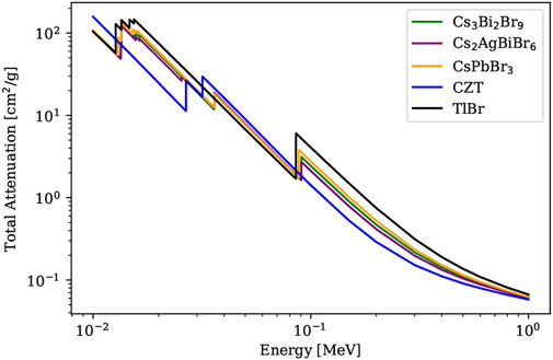
FIGURE 1. Energy-dependent total attenuation cross-section of Cs3Bi2Br9 along with contemporary inorganic perovskites and semiconductor detector materials (XCOM data).
Solution growth methods are widely used to grow hybrid perovskites because melt growth techniques were not viable due to the instability of organic compounds around their melting temperatures. Recent progress demonstrated that hybrid perovskites of millimeter to centimeter dimensions can be achieved using different solution-based growth methods at low temperatures [4]. In contrast, inorganic perovskites have higher temperature stability, and thus melt growth methods have been attempted as well [5, 6]. However, compared with melt growth, low-temperature solution growth can avoid phase transitions and advantageously provide an alternative low-cost manufacturing technique.
While advantageous, solution-based methods are often accompanied by the formation of equilibrium defects, and an increase in the concentration of vacancies, especially at higher temperatures. An underutilized, inexpensive, and scalable alternative technique of growing functional crystals named the “gel growth method” allows for controlled diffusion of reagents in a gel medium, thus facilitating the growth of high quality functional material single crystals [7]. This method has several advantages over other crystal growth methods, namely,: less chance of formation of equilibrium defects [8], lower concentration of non-equilibrium defects [9], and simplicity of growth processes. A gel can be considered a loosely interlined polymer. The most common gels for single crystal growth are silica, gelatin, and agar. The growth in silica successfully yielded very high quality crystals [9]. Gel growth methods have been demonstrated to grow functional materials such as nonlinear optical (NLO) materials, pharmaceutical crystals, nanosheets, and nanoparticles (e.g., CdS and ZnS) [7]. Additionally, the microgravity-like environment of gel growth allows one to simulate space-like environments to explore the discovery and growth of new functional crystals for a wide range of applications [7, 10].
The gel medium which effectively separates reagents also acts as an in situ filter that prevents solid particles from participating in the diffusion process as they are trapped in gel walls during gelling [7]. Moreover, crystals grown in the bulk of the gel medium has limited contact with ampoule walls and other crystals, thus eliminating potential growth stress and adhesions [8]. Additionally, the surrounding gel media limits the buoyancy-driven convection phenomenon during the growth process. The chemically inert gel medium which prevents turbulences, an advantage for keeping as-grown crystals in position, provides an ideal framework for stable nucleation and growth. In the diffusion process that leads to crystal growth, different grains from various nucleation sites compete for the solute atoms, which restrict the sizes of individual grains/crystals. Therefore, nucleation suppression is important to initiate as few crystals as possible, which advances the growth of large crystals. It has been established that the modification of gel age does decrease the diffusion rate of reactants without hindering the crystal quality, unlike the modifications of gel density and pH value [9]. Figure 2 shows a simple diagram where a U-shaped tube arrangement allows a double diffusion technique by separating two reagents with an inactive gel. In general, the methods of growing crystals in gel are very versatile and there exist different complex setups that can be used for the growth of perovskite materials in gel for radiation detector applications.
2 Methods and characterization
2.1 Chemicals
Cesium bromide (CsBr: 99.9%, Alfa Aesar), Bismuth III) bromide (BiBr3: 99%, Alfa Aesar), and Hydrobromic acid (HBr: 47%–49% in H2O, Alfa Aesar) were used in this work. Water glass solution (WGS) was prepared from sodium silicate solution Na2SiO3.9H2O (40°–42° Be, Carolina Biological) with distilled water as a solvent with the desired solution density of 1.06 g/cm3.
2.2 Gel growth
Custom-designed beakers (Total volume intake = 145 mL) with three-outlet capacities were used to form a gel matrix using an optimized gel formation HBr: WGS ratio of 1:1 with an HBr molarity of 0.67. HBr was used for gel formation when growing Cs3Bi2Br9 to prepare a gel convenient to the feeding solutions which also employ HBr as a solvent. This precaution was made to eliminate potential foreign ions, from other solvents, embedded in the gel matrix to interact with the diffusion process and thus affect the crystal formation, chemical compositions, or crystalline quality. Initially separated, a stirring of the WGS and the diluted HBr acid solution was applied inside the growth vessel, and the gel formed within 15 min. The custom-designed beakers were then covered with a layer of parafilm to avoid contamination during complete gel conversion, which took approximately 24 h.
2.3 Cs3Bi2Br9 crystal formation
Solutions of CsBr and BiBr3 were prepared with HBr separately. A gel period of 24 h and 48 h were used for two U-tube trial experiments. A dual diffusion gel growth technique was implemented where CsBr solutions were poured in the arms of the U-tube and BiBr3 solutions were poured in the center portion of the U-tube. Within a week, crystals were forming for both experiments.
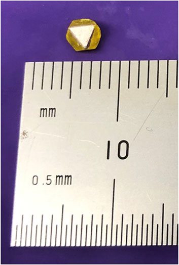
Through both trials we have successfully grown single crystals and polycrystalline crystals, which are of transparent bright green color. Even though a day apart, the 48 h gel period trial clearly shows the difference of crystal growth in sizes and quantities. As mentioned previously, one can observe that with a slower diffusion growth, the number of crystals will decrease, which allows for growth of larger crystals. Moreover, the formation of polycrystalline crystals can be attributed to high concentration of precursors used in the trial experiments where multiple crystals grew on other tiny crystals that also served as nucleation sites.
3 Results and discussion
3.1 Powder and single crystal X-ray diffraction
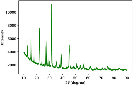
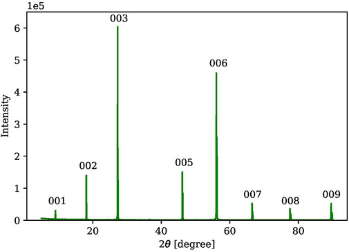
The powder X-ray diffraction (PXRD) measurements were performed using a Rigaku SmartLab X-ray diffractometer with a CuKα source at the Analytical Instrumentation Facility (AIF) of North Carolina State University (NCSU). Figure 3 shows a representative PXRD result of a gel-grown Cs3Bi2Br9 single crystal crushed into powder, which is confirmed by reference pattern (Reference code#: 00-044–0714) with a hexagonal crystal system and of space group (P-3m1). Single X-ray diffraction (SXRD) measurements were also utilized to determine the flat face of the as-grown single crystals in the gel, as shown in Figure 4.
3.2 Bandgap measurements
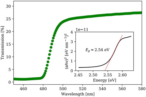
After confirmation from PXRD of the as-grown crystals, the UV-vis transmission spectrum was recorded using a light source (combination of deuterium and halogen lamps) to determine the bandgap of selected crystals. The minimum photon energy required to produce an electron/hole pair needed for electrons in the valence to be excited to the conduction band leads to an increase in the transmission spectrum at the fundamental absorption photon energy. The transmission refers to the amount of light that successfully passed through the substance material while the absorbance refers to the light that has been absorbed. The relationship between transmission and absorbance can be described by Eq. 2. The so-called Tauc plot can accurately determine the bandgap by reconstructing the transmission spectrum through reducing effects resulting from band-tailing due to material defects, described by Eq. 3, where
Figure 5 shows the spectrum of transmission vs. wavelength with an inset figure of the Tauc plot (
3.3 Device fabrication and tests
Once the material bandgap was determined, a selected Cs3Bi2Br9 single crystal with an estimated dimensions of 2 mm2 × 1.9 mm
In this step, removal of any remaining silica gel on the selected Cs3Bi2Br9 single crystal was thoroughly performed with cotton swaps. Next, silver electrodes were carefully deposited on the top and bottom surfaces of the crystal. The time frame for the remaining measurements performed under an electric field was short enough to reassure no silver electrode degradation as it is aimed in our research scope for early-stage demonstration of X-ray response.
3.4 I-V/I-V hysteresis measurement
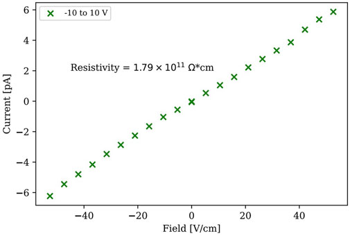
Bulk resistivity usually can be determined by measuring the current-voltage (I-V) curve, from which the resistivity can be calculated by,
where
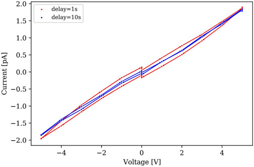
An analysis known as I-V hysteresis was also performed where voltage sweeps in the same range of approximate time frame expose the effect of slow moving mobile ions on charge collection, an established phenomena observed in past studies [13]. Furthermore, a study of high efficiency perovskite solar cells with small I-V curve hysteresis shows that I-V curve hysteresis depends on contact quality (amount of surface recombination) and the diffusion length of charge carriers [13]. A voltage sweep from -5V to 5V and back to -5V was made with different delay times. The delay time represents a varied wait time to record the succeeding current value at the given voltage value, essentially charge collection. The step sizes in the total voltage range can be varied manually as well in the command script. Figure 8 shows the I-V hysteresis in the mentioned voltage sweeps with varied delayed time from 1 s to 10 s. The I-V hysteresis shows that the varied wait time does not significantly change the current values during voltage sweeps, indicating good contact behaviors.
3.5 Mechanical properties
The mechanical properties of a Cs3Bi2Br9 single crystal grown in the gel were estimated by nano-indentation measurements that utilized a diamond indenter tip available at the AIF. Figure 9 shows the relationship between applied load and displacement for five indentation experiments performed at room temperature. Young’s modulus and hardness values were extracted using the Oliver-Phar analysis,
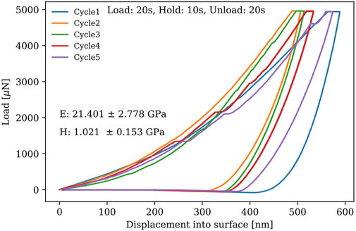
FIGURE 9. Applied load for 20s, held for 10s at 5,000 μN, and unload for 20s on a Cs3Bi2Br9 single crystal.
3.6 X-ray response
A Cs3Bi2Br9 single crystal has a strong attenuation coefficient in which 1 mm of thickness can attenuate 98.1% of incident 50 keV X-ray photons [2]. Figure 10 presents the X-ray induced response (X-ray Tube Voltage: 50 kV, X-ray Tube current: 140 mA) of a Cs3Bi2Br9 single crystal device using ON/OFF testing for 20-s periods. The X-ray response tests were performed in a non-vacuum-enclosed chamber. The X-ray tube has a Tungsten anode (10W/70 kV capability) that outputs a characteristic X-ray energy spectrum, thus not mono-energetic, under 40 keV with major intensities around 10 keV. As a low-intensity X-ray beam, the air discharge effect will not be an issue for detector measurements. The X-ray response tests were conducted under varied applied positive bias voltages using a Keithley instrument to acquire the current signals. The device was first tested under low applied voltages of 5 V and −5 V, as shown in Figure 10. The signal was higher under the positive applied field. Therefore, positive bias voltages were carried out for the On/OFF testing. Such an increase of photocurrent under the increased bias voltages, when the X-ray beam was turned on, indicates attractive responsive characteristics for X-ray photons (rise and fall time:
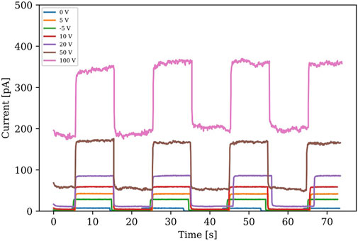
FIGURE 10. X-ray induced response (X-ray tube at 50 kV and 140 mA) under varied applied bias voltage of a Ag/Cs3Bi2Br9/Ag device.
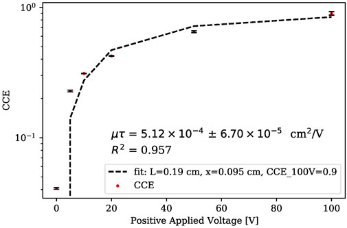
When utilizing alpha particles, a modified version of Hecht’s equation can also be represented by a single charge carrier where charge carriers will mostly be produced near an electrode. With the corresponding experimental configuration setup for cathode or anode collection, a single charge carrier travel length is effectively the detector thickness, as described by Eq. 5
where
From the net induced current (
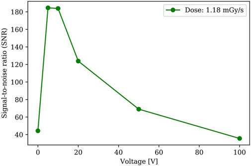
Figure 12 shows the relationship between the applied bias voltage and the signal-to-noise ratio (SNR) of the Ag/Cs3Bi2Br9/Ag device under a dose of
where
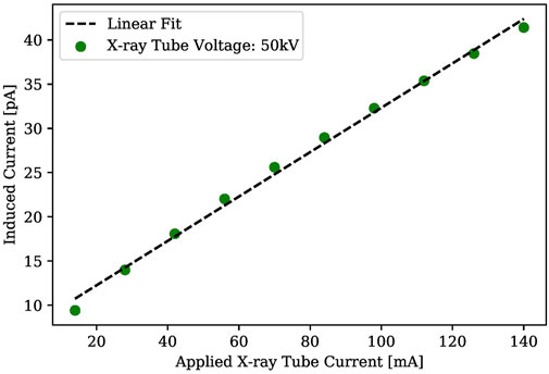
FIGURE 13. X-ray induced current of an Ag/Cs3Bi2Br9/Ag device using of varied X-ray tube current (X-ray Tube Voltage: 50kV, Bias voltage: 5V).
4 Summary
In summary, the gel growth method was utilized to grow Cs3Bi2Br9 single crystals for the first time. Our gel growth method used silica gel as a porous medium to grow single crystals, which are free of major defects with minimal Si inclusions in the diffusion process. The reagents were separated and the diffusion rate was controlled during the growth of Cs3Bi2Br9 single crystals. The diffusion starting positions were made to fasten the diffusion process in order to observe the sequent effects on growth of crystals. The PXRD results confirmed that Cs3Bi2Br9 single crystals were successfully grown in gel, which are of a hexagonal crystal system and of space group (P-3m1). The mechanical properties of as-grown Cs3Bi2Br9 single crystals were estimated using nano-indentation experiments which gave Young’s modulus of 21.401 GPa and hardness of 1.021 GPa. The device fabrication was implemented using silver electrodes. The Cs3Bi2Br9 single crystals grown in gel showed a very high resistivity,
Data availability statement
The original contributions presented in the study are included in the article/supplementary material further inquiries can be directed to the corresponding author.
Author contributions
SA: Investigation, Formal analysis, Writing—original draft. DC: Investigation, Writing—review and editing. DK: Investigation, Writing—review and editing. GY: Conceptualization, Investigation, Supervision, Writing—review and editing.
Funding
The work was performed in part at the Analytical Instrumentation Facility (AIF) of North Carolina State University, which is supported by the State of North Carolina and the National Science Foundation (award number ECCS-1542015). AIF is a member of the North Carolina Research Triangle Nanotechnology Network (RTNN), a site in the National Nanotechnology Coordinated Infrastructure (NNCI).
Acknowledgments
The gel growth discussions with Ibrahim Hany and Bryant Kanies are acknowledged. SA would like to thank his employer King Abdulaziz City for Science and Technology (KACST) for sponsoring him toward his PhD.
Conflict of interest
The authors declare that the research was conducted in the absence of any commercial or financial relationships that could be construed as a potential conflict of interest.
Publisher’s note
All claims expressed in this article are solely those of the authors and do not necessarily represent those of their affiliated organizations, or those of the publisher, the editors and the reviewers. Any product that may be evaluated in this article, or claim that may be made by its manufacturer, is not guaranteed or endorsed by the publisher.
References
1. Kakavelakis G, Gedda M, Panagiotopoulos A, Kymakis E, Anthopoulos TD, Petridis K. Metal halide perovskites for high-energy radiation detection. 305 Adv Sci (2020) 7:2002098. doi:10.1002/advs.202002098
2. Li X, Du X, Zhang P, Hua Y, Liu L, Niu G, et al. Lead-free halide perovskite Cs3Bi2Br9 single crystals for high-performance X-ray detection. Sci China Mater (2021) 64:1427–36. doi:10.1007/s40843-020-1553-8
3. McCall KM. Synthesis, crystal growth, and optoelectronic characterization of 310 inorganic halide perovskites as semiconductors for hard radiation detection. Northwestern University, Evanston, Illinois (2019).
4. Rakita Y, Kedem N, Gupta S, Sadhanala A, Kalchenko V, Bohm ML, et al. Low-temperature solution-grown CsPbBr 3 single crystals and their characterization. Cryst Growth Des (2016) 16(10):5717–25. doi:10.1021/acs.cgd.6b00764
5. Stoumpos CC, Malliakas CD, Peters JA, Liu Z, Sebastian M, Im J, et al. Crystal growth of the perovskite semiconductor CsPbBr 3: A new material for high-energy radiation detection. Cryst Growth Des (2013) 13(7):2722–7. doi:10.1021/cg400645t
6. Kobayashi M, Omata K, Sugimoto S, Tamagawa Y, Kuroiwa T, Asada H, et al. Scintillation characteristics of CsPbCl3 single crystals. Nucl Instrum Methods Phys Res Sect Accel Spectrometers Detect Assoc Equip (2008) 592(3):369–73. doi:10.1016/j.nima.2008.04.079
7. Hany I, Kanies B, Yang G. Controllable solute-diffusion gel-growth of BCHT: An effective approach towards large functional material single crystal synthesis. CrystEngComm (2020) 22(36):5954–60. doi:10.1039/D0CE00800A
8. Ahmad N, Ahmad MM, Kotru PN. Single crystal growth by gel technique and characterization of lithium hydrogen tartrate. J Cryst Growth (2015) 412:72–9. doi:10.1016/j.jcrysgro.2014.11.034
9. Patel AR, Venkateswara Rao A. Crystal growth in gel media. Bull Mater Sci (1982) 4(5):527–48. doi:10.1007/BF02824961
10. Aggarwal MD, Batra AK, Lal RB, Penn BG, Frazier DO. Bulk single crystals grown from solution on Earth and in microgravity. In: Springer handbook of crystal growth. Berlin, Heidelberg: Springer (2010). p. 559–98.
11. Ahmed I. H. (2020). Development of low power, efficient, and radiation-resistant radiation detector based on iron-doped gallium oxide, Raleigh, North Carolina.
12. Neukom MT, Züfle S, Knapp E, Makha M, Hany R, Ruhstaller B. Why perovskite solar cells with high efficiency show small IV-curve hysteresis. Sol Energ Mater. Sol. Cell (2017) 169:159–66. doi:10.1016/j.solmat.2017.05.021
13. Rakita Y, Cohen SR, Kedem NK, Hodes G, Cahen D. Mechanical properties of APbX3 (A = Cs or CH3NH3; X= I or Br) perovskite single crystals. MRS Commun (2015) 5(4):623–9. doi:10.1557/mrc.2015.69
14. Pan L, Feng Y, Kandlakunta P, Huang J, Cao LR. Performance of perovskite CsPbBr 3 single crystal detector for gamma-ray detection. IEEE Trans Nucl Sci (2020) 67(2):443–9. doi:10.1109/TNS.2020.2964306
Keywords: perovskite, Cs3Bi2Br9, gel growth, dual-diffusion, single crystals
Citation: Alshogeathri S, Cao D, Kim D and Yang G (2023) Gel growth and characterization of Cs3Bi2Br9 perovskite single crystals for radiation detection. Front. Phys. 11:1129301. doi: 10.3389/fphy.2023.1129301
Received: 21 December 2022; Accepted: 17 February 2023;
Published: 03 March 2023.
Edited by:
Kai Wang, Sun Yat-sen University, ChinaReviewed by:
Stephen A. Payne, Lawrence Livermore National Security, United StatesPushpendra Kumar, Manipal University Jaipur, India
Copyright © 2023 Alshogeathri, Cao, Kim and Yang. This is an open-access article distributed under the terms of the Creative Commons Attribution License (CC BY). The use, distribution or reproduction in other forums is permitted, provided the original author(s) and the copyright owner(s) are credited and that the original publication in this journal is cited, in accordance with accepted academic practice. No use, distribution or reproduction is permitted which does not comply with these terms.
*Correspondence: Ge Yang, Z3lhbmc5QG5jc3UuZWR1
 Saqr Alshogeathri
 Da Cao
 Doup Kim
 Ge Yang
