 Qiao Wang1
 Hualong Wu
95% of researchers rate our articles as excellent or good
Learn more about the work of our research integrity team to safeguard the quality of each article we publish.
Find out more
ORIGINAL RESEARCH article
Front. Phys. , 24 January 2023
Sec. Interdisciplinary Physics
Volume 11 - 2023 | https://doi.org/10.3389/fphy.2023.1118946
This article is part of the Research Topic Preparation and Physics of Single-crystalline Ultra-wide Bandgap Semiconductors View all 5 articles
The internal quantum efficiency (IQE) of conventional AlGaN-based deep-ultraviolet (DUV) light-emitting diodes (LEDs) is seriously limited by the poor and inhomogeneous carrier injection. The typical solution is to optimize the structure parameters of p-type region and active region. In this work, however, we try to address this issue by introducing an n-type electron deceleration layer (EDL) underneath multiple quantum wells (MQWs). On one hand, the electron deceleration layer helps to decrease the electron velocity and thus increase the electron capture rate. On the other hand, it can also reduce barrier heights in the band valence and thus enhance the hole transport in the multiple quantum wells. As a consequence, the concentrations of electrons and holes in the multiple quantum wells were significantly increased, resulting in the enhancement of radiative recombination. Compared to the conventional structure, the DUV-LED structure with an electron deceleration layer achieves a higher internal quantum efficiency, leading to a 39% improvement in the light output power. It is believed that performing energy-band engineering in n-type region has great application prospects for high-performance DUV-LEDs.
Recently, III-nitride deep-ultraviolet (DUV) light-emitting diodes (LEDs) have been regarded as the most suitable successors to displace mercury lamps because of their advantages in water purifying systems, medical devices, air sterilization and biological detection [1–4]. Compared to the commercial high-brightness blue LEDs, conventional DUV-LEDs still sustain poor internal quantum efficiency (IQE) [5, 6]. One important reason is that high-density threading dislocations in Al-rich materials dramatically reduce radiative recombination efficiency by acting as non-radiative recombination centers [7, 8]. The other primary factor is that the poor carrier injection results in the reduction of recombination proportion in the active region [5, 9–12]. To overcome this challenge, some designs have been proposed, e.g. optimization of quantum well (QW) width [13], staggered QWs [14], gradually increased quantum barrier (QB) thickness [11], graded QBs [15], graded-Al-composition last QB [16] and proper electron blocking layer (EBL) designs [17–20]. These methods primarily focus on designing proper active region and p-type EBL to alleviate electron leakage into the p-type layer and enhance hole injection into active region. In fact, the design of n-type layer also plays an important part in improving the performance in GaN-based blue and green LEDs. In terms of crystal growth, on one hand, the new design in the n-type region is more easily realized compared to those in the active region and p-type region. On the other hand, modulating n-type region facilitates the relaxation of stress and the improvement of crystalline quality. From the aspect of energy-band engineering, a proper design of n-type region can improve optoelectronic performance. Ali and Xing et al. reported an effective advantage of relaxing the stress and improving the blue LED quality by introducing a 200-nm n-Al0.03Ga0.97N underlayer and n-InGaN/GaN superlattice layer, respectively [21, 22]. Xing and Jang et al. reported that the electron capture efficiency in blue LEDs can be enhanced by introducing an n-AlGaN or graded n-InGaN layer before the growth of multiple quantum wells MQWs [23, 24]. Park et al. reported that an n-type graded-superlattice layer in green LEDs not only acts as a stress-relaxing buffer layer to release the residual stress in active region, but also acts as an electron cooler to enhance the electron capture rate in active region [25]. The above studies prove that a proper design of n-type region has great advantage in improving the crystalline quality and optoelectronic performance of blue and green LEDs. However, there are few reports on the design of n-type layer for DUV-LEDs.
In this study, a novel DUV-LED structure with an n-type electron deceleration layer (EDL) is proposed. This structure can effectively modulate the electron distribution by increasing the electron capture efficiency. Simultaneously, it can pull up the valence band of MQWs to improve hole transport. Through such an energy-band engineering, DUV-LEDs with improved radiative recombination rate and IQE were achieved.
Four DUV LED structures (Figure 1) were designed, denoted as the Original, D1, D2, and D3. The optoelectronic performances of DUV LEDs were simulated using the Advanced Physical Model of Semiconductor Devices package from the Crosslight software, based on a Schrödinger-Poisson solver method. The Original LED was designed on a c-plane sapphire substrate, consisting of a 2.5-um-thick AlN template, a 3-µm-thick n-Al0.55Ga0.45N layer (electron concentration: 6 × 1018 cm−3), 5-pair 2-nm-thick Al0.45Ga0.55N/10-nm-thick Al0.55Ga0.45N MQWs, followed by a 10-nm-thick p-Al0.60Ga0.40N EBL (hole concentration: 3 × 1018 cm−3). Finally, the structure was capped by a 10-nm-thick p-Al0.55Ga0.45N layer (hole concentration: 5 × 017 cm−3) and followed by a 100-nm-thick p-GaN (hole concentration: 1 × 1018 cm−3) layer. D1-D3 have the same design with the original LED except for the EDL. The D1 EDL is composed of Al0.48Ga0.52N (12.0 nm). The D2 EDL is composed of Al0.56Ga0.44N (4.0 nm)/Al0.48Ga0.52N (4.0 nm)/Al0.56Ga0.44N (4.0 nm). The D3 EDL is composed of Al0.56Ga0.44N (2.4 nm)/Al0.52Ga0.48N (2.4 nm)/Al0.48Ga0.52N (2.4 nm)/Al0.52Ga0.48N (2.4 nm)/Al0.56 Ga0.44N (2.4 nm).

FIGURE 1. (Color online) Schematic diagrams of AlGaN-based DUV LEDs with Original, D1, D2, and D3.
The Shockley-Read-Hall lifetime was chosen to be 10.0 ns in the simulations [26]. The internal background loss was set as 2000 m−1 [27, 28]. Because of the polarization effect, the polarization charge of the built-in interface calculated by Fiorentini et al. was reduced by a factor of 0.4 [10, 29]. The Auger recombination coefficient was set to 1 × 10–30 cm6 s−1, and the operating temperature was 300 K [5]. The energy band-offset ratio at the AlGaN/AlGaN heterojunctions was set to 0.7/0.3 [30]. The other model parameters used in the simulation can be referenced [31, 32].
The IQE and LOP curves concerning the driven current are plotted in Figures 2A, B, respectively. From Figure 2A, we can see that D3 obtains the maximum IQE of 41.74%, however, the IQEs of the original device, D1 and D2 are 29.57%, 32.96% and 36.81%, respectively. Figure 2B shows that the LOPs of the four devices increase linearly with the current injection. The LOPs of the Original, D1, D2 and D3 LEDs are 24.60, 27.21, 30.26, and 34.23 mW at 200 mA, respectively. Obviously, compared to the original LED, D3 exhibits a superior LOP with an improved coefficient of 1.39.
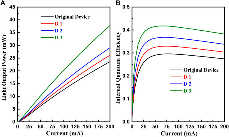
FIGURE 2. (Color online) (A) LOP and (B) IQE under different current of four devices.
These results suggest that D3 achieved the highest IQE and LOP due to the introduction of a proper EDL.
Figure 3 depicts the energy band diagrams of four LEDs to exhibit the origin of enhanced optoelectronic performance. The green region represents the EDL area. ΔEc1 is defined as the maximum potential barrier height for an electron in the front of the first QB. It can be seen that the values of ΔEc1 are quite different due to the different spontaneous and piezoelectric polarization caused by the inserted EDLs. The calculated value of ΔEc1 for the original device is only 32.60 meV. By inserting the new EDL layers, the values of ΔEc1 for D1, D2, and D3 significantly increase to 155.90, 156.19, and 157.99 meV, respectively. ΔEc2 is defined as the first potential barrier height for electrons in the MQWs along the growth direction. Since the four devices have the same structure parameter in the first QB, the values of ΔEc2 do not change much. The calculated values of ΔEc2 for the original device, D1, D2, and D3 are 117.97, 119.76, 118.01 and 115.91 meV, respectively. The electron injected from n-type layer into MQWs will go across ΔEc1 and ΔEc2 successively. Therefore, the electron blocking effect depends on the combined action of ΔEc1 and ΔEc2. Obviously, compared with the electron blocking effect of the original device, that of D3 is significantly enhanced, which decelerates the velocity of electrons. Besides, the electrons have also been stored in EDL (depicted by an orange arrow), further decelerating the velocity of electrons. To understand the effect of the inserted EDL on the holes in the active region, we take the middle QW as an example. The hole potential heights ΔEv of these four structures are 152.98, 151.04, 149.42, and 147.72 meV, respectively. In this regard, the new design can also pull up the valence band of QBs to promote hole transport. Compared to the original LED, the LEDs with EDL not only present higher barrier heights for electrons, but also lower barrier heights for holes. Thus, the electron-hole injection efficiency can be simultaneously improved via effective structural designs.
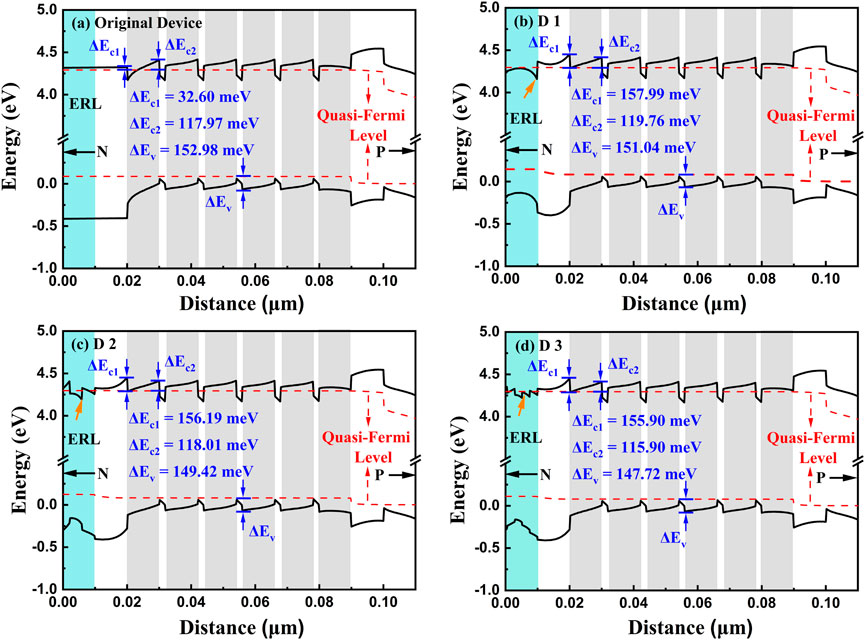
FIGURE 3. (Color online) The calculated energy band diagrams of (A) the original device, (B) D1, (C) D2, and (D) D3 at 200 mA.
Figures 4A, B depict the electron and hole concentration distributions in these LEDs at 200 mA. The electron and hole concentrations of D1, D2, and D3 MQWs are all higher than those of the original device. As calculated, the electron concentration of D3 increased by 18.25% compared to the original device. At the same time, the hole concentration of D3 is higher than that of the original LED by 22.01%. Figure 4C displays the calculated electrostatic fields of the four structures to investigate the carrier’s radiative recombination in the MQWs. The electrostatic fields exist due to the strong polarization induced by the lattice mismatch. It can be observed that the electrostatic field of the original device is higher than those of D1-D3. The existence of strong electrostatic field in the original device deteriorated IQE by decreasing wave function overlap of electrons and holes, which is known as Quantum-confinement Stark Effect (QCSE). The lower electrostatic field in D1-D3 LEDs helps to increase the overlap of electron-hole wave functions, and then it can improve the radiative recombination efficiency.
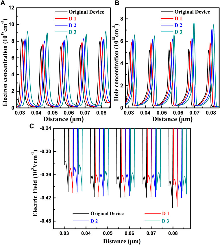
FIGURE 4. (Color online) (A) electron and (B) hole concentration of four structures at 200 mA. (C) The electric field of four devices in the active region at 200 mA.
Figure 5A demonstrates the radiative recombination rates in the active region of the four structures at 200 mA. D3 shows a much higher radiative recombination rate than the original LED. The improved radiative recombination rate can be attributed to the increase of carrier concentration and the decrease of the electric field in the active region. It is consistent with the previously mentioned energy band diagrams, carrier distribution, and electric field. Figure 5B shows the spontaneous emission spectra of four designed structures at an injection current of 200 mA. The spectral peak intensity of the D3 is nearly 1.59 times that of the original LED. At the same time, the peak emission wavelengths of the four samples are at 288 nm, indicating that the new structural design has no influence on the wavelength.
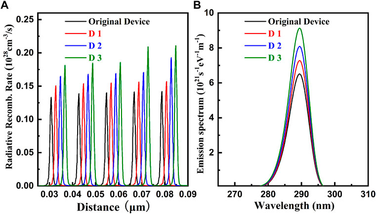
FIGURE 5. (Color online) (A) Radiative Recombination Rate and (B) Emission spectrum of four devices at 200 mA.
We have numerically analyzed the impact of an n-type EDL on the energy-band engineering for DUV-LEDs. The optoelectronic performances of the DUV-LEDs were remarkably improved, including the radiative recombination efficiency, IQE, and LOP. Introducing an EDL not only increases the potential barrier height for the electrons but also pulls up the QB valence band, which significantly modulates the carrier distribution. This can improve CIE and the radiative recombination rate, compared to the original structure. Therefore, the proposed device architectures in this study should help the community to fabricate high-efficiency DUV-LEDs.
The original contributions presented in the study are included in the article/Supplementary Material, further inquiries can be directed to the corresponding authors.
QW: Conceptualization, investigation, writing–original draft preparation. KZ: Visualization, writing–review and editing. DL: Investigation, data curation. XL: Investigation, formal analysis. YL: Investigation, methodology. SZ: Resources, data curation, Simulations. HW: Conceptualization, Investigation, Writing–review and editing. WZ: Resources, investigation, methodology. All authors have read and agreed to the publishedversion of the manuscript.
This work was supported by the National Natural Science Foundation of China (No. 62205071), the Key-Area Research and Development Program of Guangdong Province (Nos. 2020B010172001 and 2019B010132004), the Key-Area Research and Development Program of Guangzhou (No. 202103030002), Guangzhou Basic and Applied Basic Research Foundation (No. 202102021195) and the GDAS’ Project of Science and Technology Development (Nos. 2020GDASYL-20200103117, 2019GDASYL-0103072, and 2020GDASYL-20200104031).
The authors declare that the research was conducted in the absence of any commercial or financial relationships that could be construed as a potential conflict of interest.
All claims expressed in this article are solely those of the authors and do not necessarily represent those of their affiliated organizations, or those of the publisher, the editors and the reviewers. Any product that may be evaluated in this article, or claim that may be made by its manufacturer, is not guaranteed or endorsed by the publisher.
1. Khan A, Balakrishnan K, Katona T. Ultraviolet light-emitting diodes based on group three nitrides. Nat Photon (2008) 2:77–84. doi:10.1038/nphoton.2007.293
2. Moustakas TD, Paiella R. Optoelectronic device physics and technology of nitride semiconductors from the UV to the terahertz. Rep Prog Phys (2017) 80(10):106501. doi:10.1088/1361-6633/aa7bb2
3. He C, Zhao W, Zhang K, He L, Wu H, Liu N, et al. High-quality GaN epilayers achieved by facet-controlled epitaxial lateral overgrowth on sputtered AlN/PSS templates. ACS Appl Mater Inter (2017) 9(49):43386–92. doi:10.1021/acsami.7b14801
4. Wu H, Wu W, Zhang H, Chen Y, Wu Z, Wang G, et al. All AlGaN epitaxial structure solar-blind avalanche photodiodes with high efficiency and high gain. Appl Phys Express (2016) 9(5):052103. doi:10.7567/APEX.9.052103
5. He L, Zhao W, Zhang K, He C, Wu H, Liu N, et al. Performance enhancement of AlGaN-based 365 nm ultraviolet light-emitting diodes with a band-engineering last quantum barrier. Opt Lett (2018) 43(3):515. doi:10.1364/OL.43.000515
6. Zhang ZH, Chu C, Tian K, Zhang Y. Screen the polarization induced electric field within the MQWs for DUV LEDs. In: Deep ultraviolet LEDs. Springer Briefs in appl sci technol. Singapore: Springer (2019). doi:10.1007/978-981-13-6179-1_6
7. Liu C, Ooi YK, Islam SM, Xing H, Jena D, Zhang J. 234 nm and 246 nm AlN-Delta-GaN quantum well deep ultraviolet light-emitting diodes. Appl Phys Lett (2018) 112(1):011101. doi:10.1063/1.5007835
8. He C, Zhao W, Wu H, Zhang S, Zhang K, He L, et al. High-quality AlN film grown on sputtered AlN/sapphire via growth-mode modification. Cryst Growth Des (2018) 18(11):6816–23. doi:10.1021/acs.cgd.8b01045
9. Li L, Zhang Y, Xu S, Bi W, Zhang ZH, Kuo HC. On the hole injection for III-nitride based deep ultraviolet light-emitting diodes. Materials (2017) 10(10):1221. doi:10.3390/ma10101221
10. Zhang Z, Kou J, Chen S, Shao H, Che J, Chu C, et al. Increasing the hole energy by grading the alloy composition of the p-type electron blocking layer for very high-performance deep ultraviolet light-emitting diodes. Photon Res (2019) 7(4):B1–B6. doi:10.1364/PRJ.7.0000B1
11. Zhang Z, Chu C, Chiu C, Lu T, Li L, Zhang Y, et al. UVA light-emitting diode grown on Si substrate with enhanced electron and hole injections. Opt Lett (2017) 42(21):4533–6. doi:10.1364/OL.42.004533
12. Nam KB, Nakarmi ML, Li J, Lin JY, Jiang HX. Mg acceptor level in AlN probed by deep ultraviolet photoluminescence. Appl Phys Lett (2003) 83:878–80. doi:10.1063/1.1594833
13. Tian W, Feng ZH, Liu B, Xiong H, Zhang JB, Dai JN, et al. Numerical study of the advantages of ultraviolet light-emitting diodes with a single step quantum well as the electron blocking layer. Opt Quant Electron (2013) 45:381–7. doi:10.1007/s11082-012-9636-2
14. Park SH, Chuang SL. Comparison of zinc-blende and wurtzite GaN semiconductors with spontaneous polarization and piezoelectric field effects. J Appl Phys (2000) 87:353–64. doi:10.1063/1.371915
15. Yu H, Chen Q, Ren Z, Tian M, Long S, Dai J, et al. Enhanced performance of an AlGaN-based deep-ultraviolet LED having graded quantum well structure. IEEE Photon J (2019) 11(4):1–6. doi:10.1109/JPHOT.2019.2922280
16. He L, Zhao W, Zhang K, He C, Wu H, Liu X, et al. Marked enhancement in the efficiency of deep ultraviolet light-emitting diodes by using a AlxGa1-xN carrier reservoir layer. Appl Phys Express (2019) 12(6):062013. doi:10.7567/1882-0786/ab22df
17. Mehnke F, Kuhn C, Guttmann M, Reich C, Kolbe T, Kueller V, et al. Efficient charge carrier injection into sub-250 nm AlGaN multiple quantum well light emitting diodes. Appl Phys Lett (2014) 105(5):051113. doi:10.1063/1.4892883
18. Liu S, Ye C, Cai X, Li S, Lin W, Kang J. Performance enhancement of AlGaN deep-ultraviolet light-emitting diodes with varied superlattice barrier electron blocking layer. Appl Phys A (2016) 122:527. doi:10.1007/s00339-016-0073-0
19. Fan X, Sun H, Li X, Sun H, Zhang C, Zhang Z, et al. Efficiency improvements in AlGaN-based deep ultraviolet light-emitting diodes using inverted-V-shaped graded Al composition electron blocking layer. Superlattice Microst (2015) 88:467–73. doi:10.1016/j.spmi.2015.10.003
20. Zhang ZH, Chen SWH, Chu C, Tian K, Fang M, Zhang Y, et al. Nearly efficiency-droop-free AlGaN-based ultraviolet light-emitting diodes with a specifically designed superlattice p-type electron blocking layer for high Mg doping efficiency. Nanoscale Res Lett (2018) 13:122. doi:10.1186/s11671-018-2539-9
21. Ali AH, Bakar ASA, Egawa T, Hassan Z. InGaN-based multi-quantum well light-emitting diode structure with the insertion of superlattices under-layer. Superlattice Microst (2013) 60:201–7. doi:10.1016/j.spmi.2013.04.036
22. Xing Y, Deng J, Han J, Li J, Shen G. Improving the quantum well properties with n-type InGaN/GaN superlattices layer. Acta Phys Sin (2009) 58(1):590–5. doi:10.7498/aps.58.590
23. Jang CH, Sheu JK, Tsai CM, Chang SJ, Lai WC, Lee ML, et al. Improved performance of GaN-based blue LEDs with the InGaN insertion layer between the MQW active layer and the n-GaN cladding layer. IEEE J Quan Elect (2010) 46(4):513–7. doi:10.1109/JQE.2009.2036269
24. Park SH, Moon YT, Han DS, Park JS, Oh MS, Ahn D. High-efficiency InGaN/GaN light-emitting diodes with electron injector. Semicond Sci Technol (2012) 27(11):115003. doi:10.1088/0268-1242/27/11/115003
25. Park JY, Lee JH, Jung S, Ji T. InGaN/GaN-based green-light-emitting diodes with an inserted InGaN/GaN-graded superlattice layer. Phys Status Solidi A (2016) 213(6):1610–4. doi:10.1002/pssa.201533092
26. Wang Q, He L, Wang L, Li C, He C, Xiong D, et al. Remarkably improved photoelectric performance of AlGaN-based deep ultraviolet luminescence by using dual-triangle quantum barriers. Opt Commun (2021) 478:126380. doi:10.1016/j.optcom.2020.126380
27. Kuo YK, Chang JY, Chen FM, Shih YH, Chang HT. Numerical investigation on the carrier transport characteristics of AlGaN deep-UV light-emitting diodes. IEEE J Quan Electron (2016) 52(4):1–5. doi:10.1109/JQE.2016.2535252
28. Tian K, Chen Q, Chu C, Fang M, Li L, Zhang Y, et al. Investigations on AlGaN-based deep-ultraviolet light-emitting diodes with Si-doped quantum barriers of different doping concentrations. Phys Status Solidi RRL (2018) 12:1700346. doi:10.1002/pssr.201700346
29. Fiorentini V, Bernardini F, Ambacher O. Evidence for nonlinear macroscopic polarization in III–V nitride alloy heterostructures. Appl Phys Lett (2002) 80(7):1204–6. doi:10.1063/1.1448668
30. Wei SH, Zunger A. Valence band splittings and band offsets of AlN, GaN, and InN. Appl Phys Lett (1996) 69(18):2719–21. doi:10.1063/1.117689
31. Khan MA, Maeda N, Jo M, Akamatsu Y, Tanabe R, Yamada Y, et al. 13 mW operation of a 295–310 nm AlGaN UV-B LED with a p-AlGaN transparent contact layer for real world applications. J Mater Chem C (2019) 7:143–52. doi:10.1039/C8TC03825B
Keywords: DUV-LEDs, AlGaN, light output power, inhomogeneous carrier distribution, internal quantum efficiency
Citation: Wang Q, Zhang K, Lin D, Liang X, Liu Y, Zhang S, Wu H and Zhao W (2023) Introducing an n-type electron deceleration layer to enhance the luminous efficiency of AlGaN-based DUV-LEDs. Front. Phys. 11:1118946. doi: 10.3389/fphy.2023.1118946
Received: 08 December 2022; Accepted: 11 January 2023;
Published: 24 January 2023.
Edited by:
Ye Yuan, Songshan Lake Material Laboratory, ChinaReviewed by:
Zhiyuan He, No. 5 Electronics Research Institute of the Ministry of Industry and Information Technology, ChinaCopyright © 2023 Wang, Zhang, Lin, Liang, Liu, Zhang, Wu and Zhao. This is an open-access article distributed under the terms of the Creative Commons Attribution License (CC BY). The use, distribution or reproduction in other forums is permitted, provided the original author(s) and the copyright owner(s) are credited and that the original publication in this journal is cited, in accordance with accepted academic practice. No use, distribution or reproduction is permitted which does not comply with these terms.
*Correspondence: Shan Zhang, c3poYW5nQGd6aHUuZWR1LmNu; Hualong Wu, d3VodWFsb25nQGdkaXNpdC5jb20=; Wei Zhao, emhhb3dlaUBnZGlzaXQuY29t
Disclaimer: All claims expressed in this article are solely those of the authors and do not necessarily represent those of their affiliated organizations, or those of the publisher, the editors and the reviewers. Any product that may be evaluated in this article or claim that may be made by its manufacturer is not guaranteed or endorsed by the publisher.
Research integrity at Frontiers
Learn more about the work of our research integrity team to safeguard the quality of each article we publish.