 F. Borgato1,2
 D. Brundu3
 A. Cardini3*
 G. M. Cossu3
 G. F. Dalla Betta4,5
 M. Garau3,6L. La Delfa3
 A. Lai3
 A. Lampis3,6
 A. Loi3M. M. Obertino7,8
 G. Simi1,2
 S. Vecchi9*
- 1INFN, Sezione di Padova, Padova, Italy
- 2Dipartimento di Fisica, Università di Padova, Padova, Italy
- 3INFN, Sezione di Cagliari, Cagliari, Italy
- 4TIFPA INFN, Trento, Italy
- 5Dipartimento di Ingegneria Industriale, Università di Trento, Trento, Italy
- 6Dipartimento di Fisica dell’Università di Cagliari, Cagliari, Italy
- 7INFN, Sezione di Torino, Torino, Italy
- 8Dipartimento di Scienze Agrarie, Forestali e Alimentari, Università di Torino, Grugliasco, Italy
- 9INFN, Sezione di Ferrara, Ferrara, Italy
For the next generation of vertex detectors, the accurate measurement of the charged particle timing at the pixel level is considered to be the ultimate solution in experiments operating at very high instantaneous luminosities. This work shows that the 55 μm × 55 µm wide 150 µm thick 3D trench-type pixels, developed by the TimeSPOT Collaboration, achieve a time resolution close to 10 ps with minimum ionizing particles while maintaining a detection efficiency close to 100% when operated at a tilt angle larger than 10° from normal incidence. This record performance is obtained with software-based constant-fraction algorithms applied to signal waveforms. However, time resolutions as good as 25 ps can be achieved using a simple leading-edge discriminating technique, without any amplitude correction. Similar timing performances can also be achieved when the charged particles cross two nearby pixels if both signal amplitudes are measured. 3D trench-type pixels, as of today, are the fastest charged-particles pixel detectors available and represent a very promising solution for the future upgrade of tracking systems of many HEP experiments operating in extreme conditions.
1 Introduction
Future experiments at high-luminosity hadron colliders will require their detection systems to be able to operate in very high occupancy conditions. This is particularly true for their tracking system: Very large occupancies decrease tracking efficiencies, increase the fraction of reconstructed ghost tracks and make the primary and secondary vertices identification an extremely difficult task. ATLAS, CMS and LHCb experiments have shown that, for their future high-luminosity phases, measuring the tracks time with an accuracy of
This paper presents a systematic characterization of 3D trench-type pixels readout by a custom front-end electronics with 180 GeV/c charged hadrons from the SPS/H8 beam line. The pixel time resolution is measured with various methods to determine the time-of-arrival of each particle. The detector geometrical efficiency is quantified at various particle impact angles with respect to the normal direction. The detector timing performance is also measured when the charged particle crosses two adjacent pixels.
2 Materials and methods
2.1 TimeSPOT sensors
The TimeSPOT devices are 3D silicon pixel sensors optimized for efficient detection and accurate timing of minimum ionizing particles (MIP). Each pixel has a size of 55 μm × 55 µm and is characterized by an electrode configuration that presents two external ohmic-wall electrodes, which extend over the entire pixel matrix and provide the proper bias voltage to each pixel, and a collecting trench electrode 40 µm long and 5 µm thick (Figure 1) connected to the input of the front-end electronics. The depth of the sensitive volume is 150 μm, which ensures an efficient detection of a MIP (depositing about 2 fC) and guarantees good uniformity in the fabrication of the trenches. The collecting electrode is 135 µm deep. The resulting total pixel capacitance is about 110 fF. The time resolution of the TimeSPOT sensors has already been proven to be better than 20 ps [1]. This result is in agreement with sensors simulation and is dominated by the electronic jitter component of the front-end board used [2, 3].
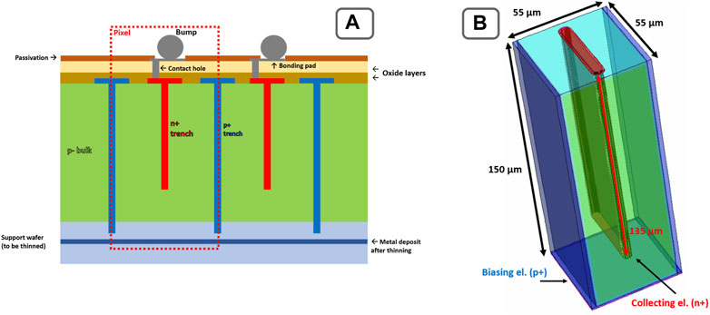
FIGURE 1. Geometry of a 3D trench-type silicon pixel. (A) Structure of a sensor and its doping profiles (red for n+ doping, green for p− doping and blue for p+ doping). (B) TimeSPOT pixel rendering with physical dimensions.
The TimeSPOT sensors studied in this paper were produced by Fondazione Bruno Kessler (FBK) in Trento, Italy, in two production runs in 2019 and 2020. The fabrication process was based on the Deep Reactive Ion Etching (DRIE) technique [4, 5]. Several test structures were produced with different geometry of readout pads, allowing the readout of a different number of pixels using single-channel front-end electronics. Three main types of sensors were characterized with particle beams: single pixels (Figure 2A), single strips consisting of 10 pixels with a common collecting electrode (Figure 2B), and a triple strip in which three adjacent pixel strips are connected to the same readout channel (Figure 2C).
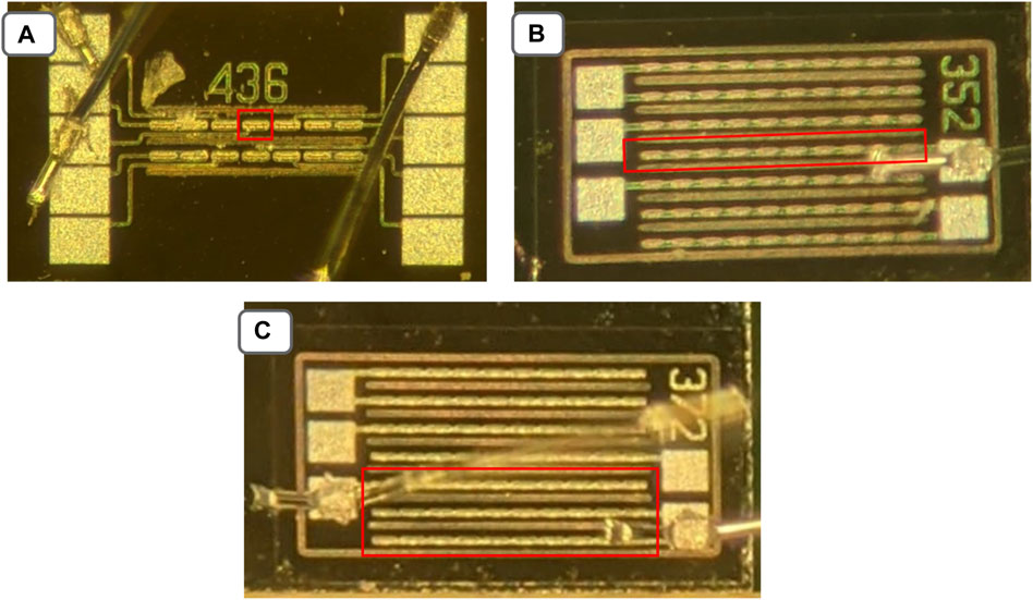
FIGURE 2. Pictures of some of the 3D-trench pixel test structures used in this work. For each structure the active area is outlined in red. (A) Single pixel sensor; (B) strip sensor (10 adjacent pixels located on the same row); (C) triple strip sensor (30 pixels located in three adjacent rows).
For single pixel studies the test structure used has seven adjacent pixels in a row (Figure 2A), where the three innermost can be individually readout. In all the measurements the two pixels next to the pixel under test are either connected to ground, to guarantee the pixel proper electric field configuration, or are connected to two additional readout channels, to allow the measurement of the charge sharing between pixels of the same row.
2.2 Front-end electronics
Front-end electronics has a crucial role in establishing the final precision of the time measurement. The impact of the electronics jitter on the total time resolution and its relationship with respect to the intrinsic time resolution of the sensor was already studied by our group [1, 2]. Our previous measurements on 3D-trench sensors timing performance show that the front-end stage is the main limiting factor to the time resolution of the complete measuring system, made of a sensor and a signal processing stage. The latter consists typically of an amplifier, a discriminating stage (fast comparator) and a digitization stage (Time-to-Digital-Converter). In the specific set-up presented in this work, the digitization stage is performed by an oscilloscope (see section 4), while the discriminating stage is performed numerically by processing the acquired waveforms.
A dedicated fast amplifier circuit, optimized to process the fast current signal output from TimeSPOT devices was developed. The circuit is based on wide-band Si-Ge bipolar transistors, having transition frequency of about 85 GHz, and a very accurate design of the board to minimize high-frequency losses of the signals. The circuit is based on a trans-impedance amplifier (TIA) scheme with two amplification stages to boost signal amplitude while keeping the noise level under control. It can be demonstrated that such a TIA scheme, using high-bandwidth components and an accurate sizing of the feedback loop, can give optimal results in timing performance [6].
This front-end electronics features a signal-to-noise ratio S/N of about 20 and an electronic jitter below 7 ps at 2 fC input charge. The amplifier rise time is smaller than 100 ps. The power consumption is about 70 mW/channel. The circuit has been produced in two versions, capable to readout either one or four sensor channels (see Figure 3). The TimeSPOT board directly houses and biases the sensor under test, which are wire bonded to the amplifier input pads. A detailed technical description of the board design and characteristics can be found in [7].
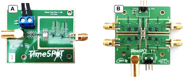
FIGURE 3. The front-end boards used in this work: (A) single-channel and (B) four-channel versions. The sensors to be readout are attached with conductive tape to the large metal pad at the board center and the readout electrodes are wire bonded to the input pad of the first stage of the amplifier. The large metal pad provides the bias to the sensor under test.
Such front-end electronics, based on high-performance discrete components, was expressly designed to accurately characterize the intrinsic time properties of single 3D-trench pixels. This approach is clearly unsuitable in the implementation of a HEP tracking apparatus, where severe system constraints are present, especially on power consumption and circuit size. In this respect, TimeSPOT is carrying on a parallel development, consisting in the design and fabrication of an ASIC in CMOS 28-nm technology. First results of such work can be found in [8].
2.3 Test beam setup
TimeSPOT sensors have been tested both in October 2021 and in May 2022 at the CERN SPS/H8 beamline with a 180 GeV/c positive hadrons beam. On average, 106 particles are extracted every 30 s in a 4 seconds-long spill and are focused on an approximately circular spot of 8 mm (sigma) radius measured at the setup location. Two 3D-trench silicon sensors on their front-end electronics (FEE) boards are mounted inside an electromagnetically shielded and light-tight box, one after the other along the beamline, as shown in Figure 4. While one of the two 3D-trench sensors is installed on a fixed mount, the other one is mounted on a movable holder driven by two closed-loop piezoelectric linear stages1 allowing maximum 16 mm movements with 10 nm position accuracy in the directions transverse to the beam line. One of the holders also allows to manually rotate the sensor around the vertical direction to measure the sensor response for non-normal beam incidence. The time-of-arrival of each particle (TOA) is measured by means of two 18 mm diameter 5.5 mm thick quartz input window microchannel-plate photo-multipliers tubes (MCP-PMTs)2.
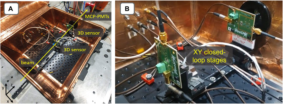
FIGURE 4. The setup used for the measurements described in this work. (A) The sensors mounted on their FEE boards inside the RF shielded and light tight box and the two MCP-PMTs downstream; (B) Closer view of the sensors inside the box. The sensor on the right is mounted on a fixed holder close to the beam entrance window. The sensor on the left is mounted on a movable holder driven by two closed-loop piezoelectric linear stages.
Signals from the silicon sensors and the two MCP-PMTs are acquired by means of an 8 GHz analog bandwidth 20 GSa/s 4 channels digital oscilloscope3. The sensors and the MCP-PMTs are connected to the oscilloscope using low-loss RF cables. The oscilloscope trigger condition is chosen on the basis of the measurement as described in section 3. A typical event acquired with this setup is shown in Figure 5.
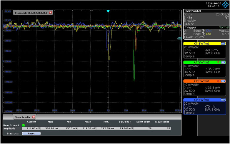
FIGURE 5. A typical event acquired during the data taking. The signals from the two silicon sensors are shown in yellow and blue, while the signals from the two MCP-PMTs are shown in green and orange. The relative timing between silicon sensors and MCP-PMTs signals is digitally adjusted to optimize the trigger condition used.
2.4 Analysis method
The TOA of each sensor signal is determined by different methods referred to as reference, Spline and Leading Edge (LE) in the following [1]. The reference method is an implementation of the amplitude and rise time compensation (ARC) method [9], where the signal waveform is delayed by about half of its rise time and a subtraction with the original waveform is performed, then the TOA is determined as the time where the resulting waveform exceeds half of its maximum amplitude. The Spline method interpolates the waveforms with cubic splines and sets the TOA to the time at which the signal exceeds a fraction (20%) of its maximum amplitude. Finally, the LE method defines the TOA as the time at which the signal amplitude exceeds a fixed threshold (15 mV): this was evaluated independently of the signal amplitude (standard LE method) and also by applying an amplitude-dependent correction to compensate for the time walk (amplitude-corrected LE method).
All the parameters of the methods (delay, all thresholds, etc.) were optimized with real data to guarantee the best detection efficiency and timing performance. These parameters are related to the characteristics of the signals (rise time, amplitude and noise) that depend on the front-end electronics and on the sensors used.
3 Results
3.1 Detection efficiency
Trenches in 3D-trench pixel sensors are non-sensitive volumes, so if a charged particle crosses the sensor inside a trench, no signal will be recorded. To obtain a full detection efficiency, 3D pixels are typically installed at a slightly tilted angle with respect to normal incidence. In this section the effect of the geometrical acceptance on the detection efficiency of 3D-trench silicon pixels is studied as a function of the tilt angle with respect to normal incidence. This measurement is performed by triggering on a single 3D-trench pixel which was precisely centered, projectively along the beam line, on a triple strip (3 adjacent strips, each made of 10 pixels each, see Figure 2C), acting as device under test (DUT). All the 30 pixels of the triple strip are connected together to the same readout channel of the single-channel front-end board (Figure 3A). A particle seen by the trigger pixel will also cross the triple strip producing a signal unless it ends up inside the trenches. The two MCP-PMTs are also readout to obtain a precise charged particle time reference. To study the effect on the geometrical acceptance due to the trench insensitive volumes, the efficiency measurement is performed at tilt angles of 0°, 5°, 10° and 20° with respect to the DUT normal incidence by rotating the DUT around the pixel-strip axis. Moreover, to minimize the overlapping of insensitive volumes, the pixel trenches were oriented perpendicularly to the triple strip trenches.
The efficiency is computed as ɛ = Nts/Ntrks, where Nts and Ntrks are the number of tracks detected by the triple strip and the tracks crossing the triple strip volume, respectively. A track is detected in case the measured TOA relative to the time reference, t3strip − ⟨tMCP-PMT⟩, is consistent with the expected value, given by the time of flight, as explained later. Such method has been proven to be successful also for small signal amplitudes, consistent with the noise level. The number of tracks crossing the triple strip volume is obtained by correcting the number of triggered signals with a minimum pulse height both in the pixel and in the MCP-PMTs in a time window of ±200 ps around the expected time difference tpixel − ⟨tMCP-PMT⟩, Ntrig, by the fraction of tracks that miss the triple strip due to the beam divergence, Ntrks = Ntrig ⋅ (1 − fmiss). This fraction is estimated using a data sample acquired with the trigger single pixel shifted by 165 µm along the short side of the triple strip and amounts to fmiss = 1.4 ± 0.6%.
Figure 6 shows the distribution of the difference between the TOA of the triple strip and the time reference for all triggered events. The number of detected tracks is determined by fitting the distribution with a peaking function given by the sum of a Gaussian and an exponential convoluted with a Gaussian, modelling the detected tracks, and a constant function, describing the undetected tracks which feature random TOA values.
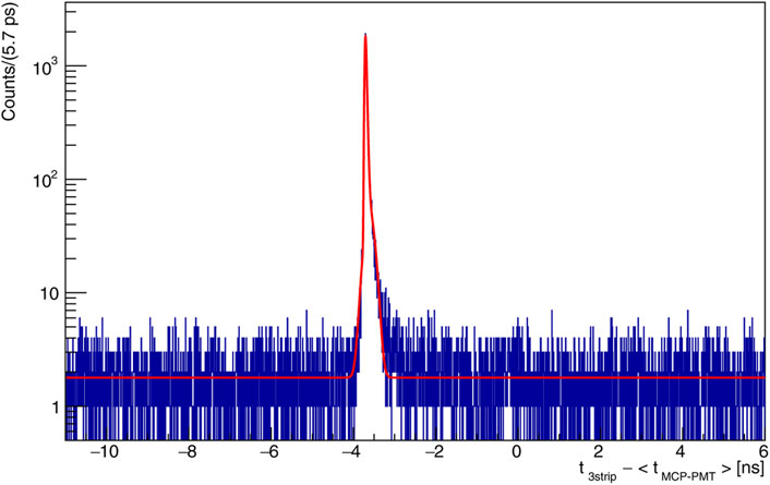
FIGURE 6. Distribution of the difference between the TOA of the triple strip and the time reference, t3strip—⟨tMCP-PMT⟩, for the triggered tracks with a minimum pulse height both in the pixel and in the MCP-PMTs in a time window of ±200 ps around the expected time difference tpixel − ⟨tMCP-PMT⟩, Ntrig. The detected tracks populate the peaking structure around −3.5 ns, while the undetected tracks are uniformly distributed. The red curve represents the result of the fit to the distribution and it is used to determine the yield of detected tracks Nts for the efficiency calculation. In particular, Nts is computed as the difference of the number of entries in the histogram and the integral of the background (constant) contribution from the fit.
At 0° incident beam angle the efficiency is measured to be ɛ = 79.2 ± 0.6%, where the uncertainty accounts for both statistical and systematic contributions. The systematic uncertainty includes uncertainties related to the different methods used to determine the TOA (section 2.4), to the choice of the fit function to calculate the yield of detected tracks and the uncertainty on the fraction fmiss. As a cross check, the efficiency is also calculated simply by counting the number of events for which the triple strip signal has an amplitude above a certain threshold. For thresholds above the noise level (
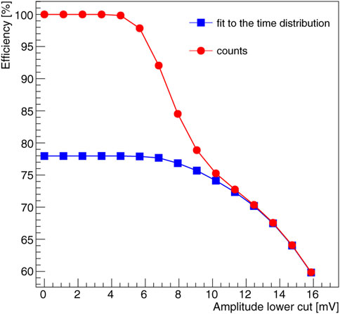
FIGURE 7. Triple strip efficiency calculated by counting the yield of signal events from a fit to the time distribution (blue) and from the number of events with the amplitude above a given threshold (red). Note that for this comparison the efficiencies are not corrected for the fraction fmiss.
The efficiency, as expected, increases as a function of the incident beam angle with respect to normal sensor incidence. The results at 5°, 10° and 20° are ɛ = 90.5 ± 0.8%, 98.3% ± 0.5% and 99.1% ± 0.5%, respectively and are also shown in Figure 8. These results are consistent with the expected triple strip geometrical acceptance, which depends on the fraction of the sensor active volume. In fact, at normal incidence, assuming that only tracks crossing the active area of the silicon sensors are detected with 100% efficiency, the geometrical acceptance of the triple strip is expected to be between 82.4% and 84.4%, assuming 5 µm wide trenches and depending on the relative alignment between the single pixel used for trigger and the DUT (and assuming a zero angular divergence beam).
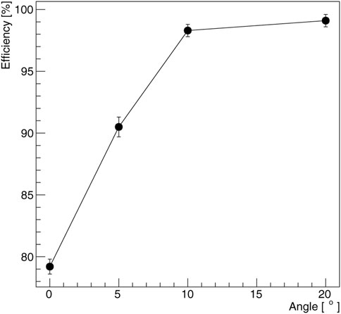
FIGURE 8. Triple strip efficiency as a function of the tilt angle with respect to normal sensor incidence. The DUT is rotated around the pixel-strip axis.
By tilting the sensor around the pixel-strip axis from normal incidence, the contributions due to particles crossing only the inactive volume of the sensor decrease and the full efficiency is restored for tilt angles just above 10°.
Of course in a real detector the detection efficiency will be reduced by the need to introduce a minimum amplitude requirement (Figure 7, blue points). The efficiency loss strongly depends on the characteristics of the front-end electronics (S/N ratio) and cannot be easily compared to other devices.
3.2 Single pixel timing performances
In this section we report the timing performance of a single 3D-trench silicon pixel operated at different bias voltages. For these measurements the acquisition was triggered by the coincidence of signals detected on a silicon strip sensor placed upstream the pixel and two MCP-PMTs located downstream. The pixel was carefully aligned in the beam transverse plane with respect to the strip in order to maximize the rate of detected coincidences. The pixel bias was varied in a wide voltage range from −7 V to −100 V. The pixel was readout by the single-channel front-end board (Figure 3A).
The TOA of the sensor is determined by means of the reference, the Spline and the LE methods. Minimal requirements on the amplitudes of the MCP-PMTs and on the strip signals are applied to reject badly reconstructed events. The timing performance of the sensor are measured with respect to the time reference given by the mean of the two MCP-PMTs TOAs, which has a precision in the range of 3 to 4 ps. Figure 9A shows the distribution of the difference between the TOA of the single pixel and the time reference, tpixel − ⟨tMCP-PMT⟩ in the time range where signals are expected for the measurement at Vbias = −100 V. The distribution consists of a peaking structure, due to energy deposits in the single pixel, and of a constant contribution, due to noise events. The peak is described by the sum of two Gaussian functions with an effective resolution of
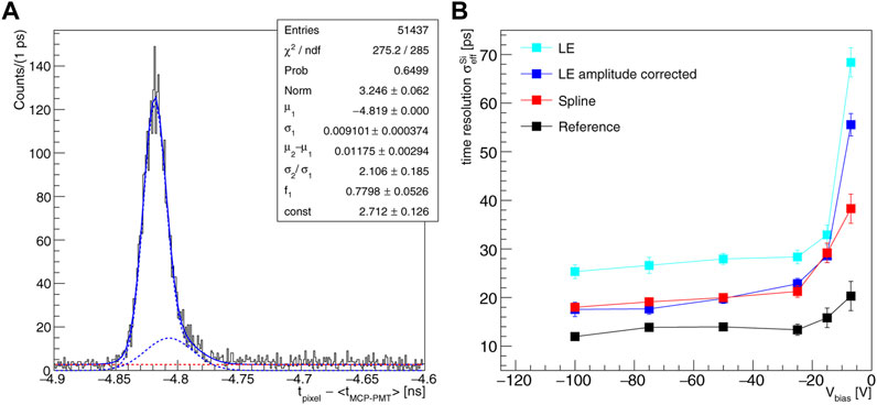
FIGURE 9. (A) Distribution of the difference between the TOA of the single pixel and the time reference, tpixel—⟨tMCP-PMT⟩, for the single pixel at Vbias = −100 V with the reference method. The distribution is fit with the sum of two Gaussian functions (blue dashed lines) describing the signal, and a constant (red dashed line) modelling the background. (B) Effective time resolution of the single pixel at different bias voltages for different analysis methods. Here the contribution due to the resolution of the time reference is subtracted.
Figure 9B shows the measured values of the effective time resolution of the single 3D-trench pixel for different bias voltages, obtained using different analysis methods. The timing performances are almost constant for Vbias < − 25 V, while they worsen rapidly for lower absolute biases. This worsening is related to both the specific, fast front-end used for these measurements, that is less efficient in collecting the full charge from slow signals, and to the increased differences of the charge carrier velocities at low absolute bias voltage that affects the sensor uniformity. The best single pixel timing performances are obtained using the reference method, thanks to its capability of minimizing the time walk caused by charge collection time variations. Also, despite its simplicity, the LE method with fixed threshold provides time resolutions below 30 ps, while the LE method corrected for the time walk performs similarly to the Spline method for Vbias ≤ −15 V.
Figure 10 shows the single pixel time resolution as a function of the signal amplitude from a large data sample where the pixel triggered the acquisition. The observed dependency is consistent with the expectations based on the assumption that both the electronic jitter, which scales with the amplitude, and a constant term, intrinsic of the sensor, contribute to the total resolution. From the values at large amplitude it is possible to infer the constant term value of ≤ 10 ps, which represents an estimate of the intrinsic time resolution of the sensor.
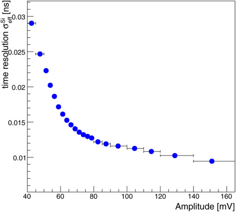
FIGURE 10. Single pixel time resolution as a function of the signal amplitude. The results are obtained from a large data sample where the pixel triggered the acquisition and the bias voltage was Vbias = −75 V. The resolution values correspond to the reference method. The value at 150 mV,
3.3 Single pixel amplitude distribution
In case of efficient sensors, the amplitude distributions are related to the energy deposit in the active area of the sensor which depends on the track length given by charged particles within the sensor volume. For an incident beam angle of 0° (normal incidence), the track length distribution can be approximated by a δ-Dirac around the active thickness of the sensor (d = 150 µm), while for an angled beam the track length distribution widens. For a particle entering the sensor structure at an angle θ with respect to normal incidence the total track length increases by a factor (cos θ)−1 but, depending on the particle impact point on the pixel surface and on the angle θ, the length of the particle path within the active volume of the pixel could also decrease in all the cases the particle crosses a trench, exits or enters into the pixel laterally. As a result the mean particle path length is maximal at 0°.
Figure 11 shows the amplitude distributions of the single pixel for incident beam angle of 0°, corresponding to the same data samples used to measure the timing performance described in the previous section. Only events in the time range ± 75 ps around the peak of the TOA distributions (as shown in Figure 9A) are selected. This requirement suppresses the background contribution that populates the region A < 20 mV. The peaking contribution above 20 mV is associated to sizable energy deposits in the sensor. The amplitude distributions follow the characteristic Landau shape. For Vbias ≤ −50 V the distributions overlaps almost perfectly, while for Vbias = −25 V, −15 V and −7 V they are shifted to lower values. The reduced signal amplitudes observed at low absolute bias voltages are due to the effect of the fast front-end electronics on the slower signals (ballistic deficit).
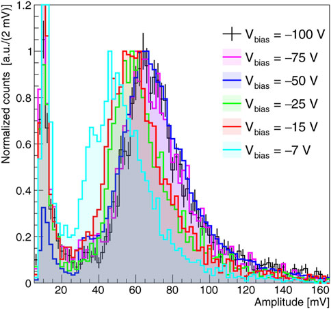
FIGURE 11. Amplitude distribution of the single pixel at normal beam incidence and for different bias voltages. The distributions are normalized at the Landau peak.
3.4 Charge sharing between adjacent pixels
Most of the results discussed so far only considered the response of a single 3D-trench pixel. However, a charged particle crossing the sensor at angles different from normal incidence typically crosses the active volumes of two adjacent pixels, and in these cases both the pixel under study and its neighboring pixels play a role in the definition of the overall performance of the system.
In this section we report the studies on the charge sharing between two adjacent pixels located on the same row for different incident beam angles. In these measurements the DUT consists of two neighbor pixels which are individually readout by the four-channel version of the front-end board (Figure 3B). The acquisition was triggered by the coincidence of a signal detected by a single pixel and a signal on one MCP-PMT placed upstream and downstream the DUT, respectively. In this case the single MCP-PMT provides the event time reference. The triggering pixel was carefully aligned on the beam line and centered on the DUT to equalize the occupancies on the two pixels. The pixels were biased at a voltage Vbias = −100 V. This setup allows to study both the performance of a single pixel alone and that of the two pixels considered as a cluster.
Depending on the impact position and on the incident angle a track can create a signal in one or both the adjacent pixels. In this study the following event categories are defined: the whole pixel, the single pixel, the shared pixel and the cluster. A whole pixel event type only needs minimal requirements on the pixel signal amplitude and TOA to reject most of the noise and any signal in the neighbor pixel is ignored. When also looking at the neighbor pixel, if there is no signal in it - by applying cuts on its signal amplitude and TOA (A < 15 mV OR |tpixel—tMCP-PMT| > 100 ps) - the event is labelled single pixel. Vice versa, if a signal on the neighbor pixel is present (A > 15 mV AND |tpixel—tMCP-PMT| < 100 ps), the event is labeled shared pixel. In this last case a cluster is made by combining the information of the two pixels. The same event could contribute to more than one of the categories above.
Figure 12A shows the amplitude distributions at 20° for the different event types. The distribution of the whole pixel events deviates from the characteristic Landau shape due to the contribution of the shared pixel events, populating the region of small amplitudes (A < 40 mV). By applying a clusterization algorithm to these events, the resulting amplitude, given by the sum of the amplitudes recorded on the two pixels, recovers the expected Landau distribution. Figure 12B shows the amplitude distributions of the clusterized pixels for all measured angles, including both the information of the single pixel events (cluster size equal to 1) and of the shared pixels after clusterization (cluster size equals to 2). The distributions overlap for A > 45 mV and peak to consistent values as expected. The differences in the distributions at low amplitudes, mostly visible at 20°, are due to the fact that at these angles events with cluster size equals to 3 become possible, so a small amount of charge could be lost in the current two-pixels setup.
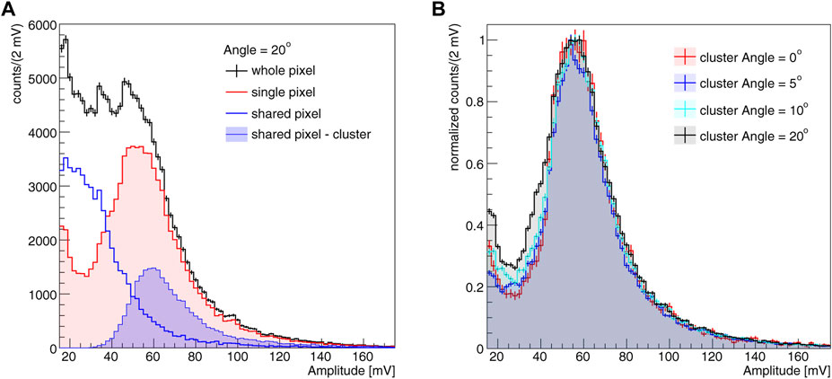
FIGURE 12. (A) Amplitude distributions at 20° with respect to normal incidence for different event categories; (B) Cluster amplitude at various particle incident angles.
Figure 13A show the TOA distributions, evaluated using the Spline method, with respect to the time reference for the different event categories, corresponding to an incident beam angle of 20°. To combine the results of the two pixels, the TOA of each pixel is corrected by its mean value determined using calibration data samples at 0° with each pixel aligned with the trigger pixel and the beam line. The distributions show clear differences in the widths depending whether the particle crosses one or two pixels. The time resolutions,
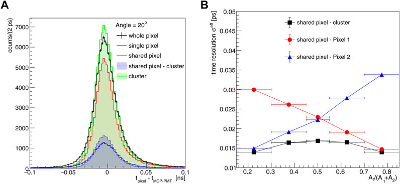
FIGURE 13. (A) Distributions of the TOA of the pixel with respect to the time reference for the different event categories; (B) Two-pixel cluster time resolution as a function of the ratio of the amplitude of one pixel to the sum of the two (black curve—See text for details). The time resolution estimated using only the individual pixel information is also shown (red and blue curves). The results correspond to an incident beam angle of 20°.
Figure 13B shows the time resolution of the two-pixel cluster as a function of the ratio of amplitudes Apixel,1/(Apixel,1 + Apixel,2) for each of the pixel forming the cluster, and the time resolution measured using only the individual pixel information. The largest improvement in time resolution due to the clusterization algorithm is reached when the amplitudes of the two pixels are similar, while in the cases when one pixel dominates over the other the time resolution of the combination is similar to that of the dominant pixel. In all cases the time resolution of the cluster is consistent with the combined resolutions of each pixel. This result implies that the resolution is not dominated by the electronic jitter contribution.
Overall, the clustering allows to recover the timing performances at normal incidence when only one pixel is hit. The measured resolutions at 5°, 10° and 20° are all consistent with the corresponding value of 20.6 ± 0.2 ps measured at 0° with the same setup and analysis method.
4 Discussion
In this work it was shown that high-energy charged-particle timing with a time resolution close to 10 ps can be achieved with TimeSPOT innovative 3D trench-type silicon pixels. This result is obtained using software-based constant-fraction discrimination algorithms on the signals processed by our custom pixel front-end electronics and represents an upper limit of the intrinsic time resolution of these innovative detectors. The timing performances of a real detector will heavily depend on the actual front-end electronics that will be implemented at the ASIC level. The use of other particle time-of-arrival measuring methods, as the more common leading-edge discrimination technique, also shows an excellent performance allowing to reach time resolutions close to 25 ps. Since the trenches in 3D pixel are an inactive detection material, pixel efficiency measurements at particles impact angles up to 20° with respect to normal incidence were performed. As seen in other types of 3D pixels, the full geometrical efficiency can be recovered by tilting the sensors at 10 or more degrees. Tilting the sensor increases the chance of having particles crossing two adjacent pixels. In this work it was also observed that the two-pixel cluster time-of-arrival distributions, obtained by performing an amplitude-based weighted average of the individual pixel time-of-arrival measurements, has a width similar to the single-pixel one for all charge sharing fractions, guaranteeing that the sensor excellent time resolution is maintained also when the charge is shared between pixels. 3D trench-type detectors, as of today, are the fastest radiation-hard and high-rate charged-particles pixel sensors available. They appear to be a very promising solution for the future upgrade of the tracking systems of many HEP experiments operating at very high instantaneous luminosities.
Data availability statement
The raw data supporting the conclusions of this article will be made available by the authors, without undue reservation.
Author contributions
GFDB, ALai and ALoi designed the sensors; DB, GMC and ALoi Performed simulation studies related to the measurements; GMC and ALai designed and realized the front-end electronics; AC, MG, LLD, and ALam designed and prepared the experimental setup; FB, AC, MG, LLD, ALai, ALam, ALoi, MMO, GS, and SV partecipated to the test beam measurements at SPS; FB, MG, ALam, MMO, GS, and SV performed the data analysis; FB, AC, GMC, MG, ALai, ALam, and SV contributed to the paper writing, and all authors reviewed it.
Funding
This work was supported by the Fifth Scientific Commission (CSN5) of the Italian National Institute for Nuclear Physics (INFN), within the Project TimeSPOT and by the ATTRACT-EU initiative, INSTANT project. This project has received funding from the European Union’s Horizon 2020 Research and Innovation program under GA no. 101004761.
Acknowledgments
The authors wish to thank the staff of North Hall Area at CERN for their help in the beam-line setup and operations.
Conflict of interest
The authors declare that the research was conducted in the absence of any commercial or financial relationships that could be construed as a potential conflict of interest.
Publisher’s note
All claims expressed in this article are solely those of the authors and do not necessarily represent those of their affiliated organizations, or those of the publisher, the editors and the reviewers. Any product that may be evaluated in this article, or claim that may be made by its manufacturer, is not guaranteed or endorsed by the publisher.
Footnotes
1High Speed Piezo Linear Stage, 16 mm Travel (model CONEX-SAG-LS16P), https://www.newport.com/p/CONEX-SAG-LS16P.
2Micro-channel plate photomultiplier (model PP23565Y) by Photonis Netherlands B.V., https://www.photonis.com/products/mcp-pmt.
3Rohde&Schwarz digital oscilloscope (model RTP084), https://www.rohde-schwarz.com/product/rtp-productstartpage_63493-469056.html.
References
1. Anderlini L, Aresti M, Bizzeti A, Boscardin M, Cardini A, Dalla Betta GF, et al. Intrinsic time resolution of 3D-trench silicon pixels for charged particle detection. J Instrumentation (2020) 15:P09029. doi:10.1088/1748-0221/15/09/p09029
2. Brundu D, Cardini A, Contu A, Cossu GM, Dalla Betta GF, Garau M, et al. Accurate modelling of 3D-trench silicon sensor with enhanced timing performance and comparison with test beam measurements. J Instrumentation (2021) 16:P09028. doi:10.1088/1748-0221/16/09/p09028
3. Brundu D, Contu A, Cossu GM, Loi A. Modeling of Solid state detectors using advanced multi-threading: The TCoDe and TFBoost simulation packages. Front Phys (2022) 10. doi:10.3389/fphy.2022.804752
4. Laermer F, Franssila S, Sainiemi L, Kolari K. Chapter 21 - Deep reactive Ion etching. Micro Nano Tech (2015) 2015:444–69. doi:10.1016/B978-0-323-29965-7.00021-X
5. Forcolin G, Boscardin M, Ficorella F, Lai A, Loi A, Mendicino R, et al. 3D trenched-electrode pixel sensors: Design, technology and initial results. Nucl Inst. Methods Phys Res Section A (2020) 981:164437. doi:10.1016/j.nima.2020.164437
6. Lai A, Cossu GM. Timing performances of front-end electronics with 3D-trench silicon sensors. J. Instrumentation (2023). arXiv:2301.11165.
7. Cossu GM, Lai A. Front-end electronics for timing with pico-seconds precision using 3D trench silicon sensors. J. Instrumentation (2023)18:P01039. arXiv:2209.11147.
8. Cadeddu S, Frontini L, Lai A, Liberali V, Piccolo L, Rivetti A, et al. Timespot1: A 28nm CMOS pixel read-out ASIC for 4D tracking at high rates (2022). arXiv:2209.13242.
9. Cho Z, Chase R. Comparative study of the timing techniques currently employed with Ge detectors. Nucl Instr Methods (1972) 98:335–47. doi:10.1016/0029-554X(72)90115-2
10. Cossu GM, Brundu D, Lai A. Intrinsic timing properties of ideal 3D-trench silicon sensor with fast front-end electronics. J. Instrumentation (2022). arXiv:2301.11190.
Keywords: particle tracking detectors, solid-state detectors, timing detectors, high time resolution, high luminosity
Citation: Borgato F, Brundu D, Cardini A, Cossu GM, Dalla Betta GF, Garau M, La Delfa L, Lai A, Lampis A, Loi A, Obertino MM, Simi G and Vecchi S (2023) Charged-particle timing with 10 ps accuracy using TimeSPOT 3D trench-type silicon pixels. Front. Phys. 11:1117575. doi: 10.3389/fphy.2023.1117575
Received: 06 December 2022; Accepted: 24 January 2023;
Published: 08 February 2023.
Edited by:
Giovanni Calderini, UMR7585 Laboratoire Physique nucléaire et Hautes Energies (LPNHE), FranceReviewed by:
Sebastian Grinstein, Institute for High Energy Physics, SpainGabriele Giacomini, Brookhaven National Laboratory (DOE), United States
Copyright © 2023 Borgato, Brundu, Cardini, Cossu, Dalla Betta, Garau, La Delfa, Lai, Lampis, Loi, Obertino, Simi and Vecchi. This is an open-access article distributed under the terms of the Creative Commons Attribution License (CC BY). The use, distribution or reproduction in other forums is permitted, provided the original author(s) and the copyright owner(s) are credited and that the original publication in this journal is cited, in accordance with accepted academic practice. No use, distribution or reproduction is permitted which does not comply with these terms.
*Correspondence: A. Cardini, YWxlc3NhbmRyby5jYXJkaW5pQGNhLmluZm4uaXQ=; S. Vecchi, dmVjY2hpQGZlLmluZm4uaXQ=