 Yuting Xu
 Zhongxing Tian1
94% of researchers rate our articles as excellent or good
Learn more about the work of our research integrity team to safeguard the quality of each article we publish.
Find out more
REVIEW article
Front. Phys., 06 September 2022
Sec. Optics and Photonics
Volume 10 - 2022 | https://doi.org/10.3389/fphy.2022.985208
This article is part of the Research TopicEditor's Challenge in Optics and Photonics: Advancing Electronics with PhotonicsView all 6 articles
The construction of large-scale integrated photonic circuit cannot be separated from the important role played by silicon-based optoelectronic devices. As a basic and important link in on-chip photon propagation, beam splitting is of great significance for the efficient utilization of sources and the compact integration of optoelectronic devices. It is widely used in power splitting, polarization separation, wavelength division multiplexing and other scenarios. This paper reviews the on-chip beam splitting methods in recent years, which are mainly divided into the following categories: y-branch, multimode interference coupling, directional coupling, and inverse design. This paper introduces their research status, including optimization design methods, functions and applications in large-scale quantum chips and optoelectronic hybrid integration, looking forward to providing a reference for the further research of beam splitting methods and the wide application of beam splitters in the frontier field in the future.
Compared with the optical system composed of traditional optical devices, the photonic integrated circuit composed of on-chip optical devices has the advantages of wide bandwidth, easy implementation of dense wavelength division multiplexing (WDM), compact structure, light weight, low energy consumption, high reliability, easy integration, and compatibility with traditional CMOS technology. Typical integrated optical systems include generation [1–4], coupling [5–34], splitting [35–81], modulation [82–98], and detection [99–102] of photons. Among them, on-chip beam splitting is not only the key link of photon propagation, but also an important part of integrated devices such as Mach Zehnder interferometer (MZI) [103, 104] and microcavity [105–107]. It is closely related to the efficient utilization of sources and low loss propogation. So far, with the support of electromagnetic theory, optical waveguide theory and coupled mode theory, researchers can design splitters with different functions according to different applications, including power splitters, polarization splitters, wavelength division multiplexers, mode multiplexers, etc. Over the years, researchers have optimized the basic beam splitting devices for many times through the application of special structural design and optimization algorithm, and realized beam splitting devices with rich functions, which laid the foundation for the construction of large-scale integrated optical systems. They are widely used in quantum sensing, quantum information processing and other fields.
Nowadays, several classical structures used for on-chip beam splitting mainly include y-branch waveguide [35–51], splitters based on multimode interference (MMI) coupling [52–69], splitters based on directional coupling (DC) [70–75], and splitters based on inverse design [76–81]. Among them, the design principle of y-branch waveguide is relatively simple, and the separation of mode and power is mainly realized through the y-type structure design. However, the y-branch power splitter of traditional waveguide is limited by the radiation loss at the branch angle, resulting in the large transverse size of the device. Therefore, the y-branch power splitter based on photonic crystal waveguide is introduced, and its branch angle can reach 120°, which greatly reduces the footprint of the devices. At the same time, splitters based on MMI is a usual beam splitting method at present. Compared with other devices, it has the advantages of lower insertion loss, wider frequency band, easier fabrication process and better tolerance. It has been widely used in optical devices such as power splitter, polarization splitter, WDM and so on. The MMI splitter uses the self-imaging effect to determine the structural parameters of the multimode waveguide, and carries out phase interference between the excited high-order modes in the incident waveguide, so as to periodically reproduce the input image along the propagation direction of the guided wave. By analyzing the propagation of the light field and following the existing design principles, multi-channel uniform power output can be realized at the output. In addition, if the beat length difference between TE and TM polarized light is required to be 0, the purpose of polarization independent design can be achieved [108]. As another important component of the beam splitting methods, the DC is composed of two similar single-mode waveguides. By using the mode coupling principle and adjusting the length of the coupling region, the basic separation of power and polarization can be achieved. Different from the above design methods based on traditional structures, the concept of inverse design has also been widely used in the design of silicon-based optoelectronic devices in recent years. In this method, an ideal target value is preset first, and then the device is programmably designed by using topology optimization [77], particle swarm optimization [81], direct binary search [76, 78] and other optimization algorithms, so as to obtain the structure that meets the functions. The splitter designed by this method is often compact and flexible, but it also has the problems of many iterations and long calculation time. Based on the above analysis, the four main beam splitting methods are compared as shown in the following Table 1.
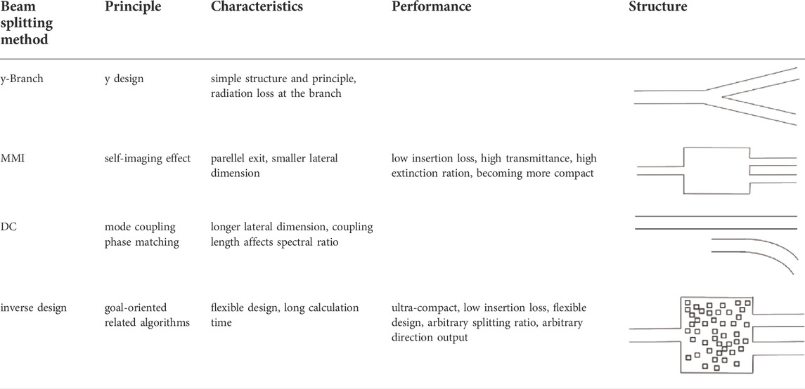
TABLE 1. Comparison of four main beam splitting methods.
In this paper, the on-chip beam splitting methods in recent years are reviewed, the research progress, optimization design methods, implementation functions and applications of several main beam splitting methods are introduced, and the applications of on-chip beam splitting in large-scale quantum chips are prospected.
As one of the most basic integrated optical devices, the y-branch waveguide is composed of one input waveguide and two output waveguides, which can confine photons to the y waveguide for distribution and propogation. On the one hand, uniform power splitting can be achieved by using the longitudinal symmetric design of the y-branch, and the basic y-branch structure can be optimized, such as replacing the common y-branch with the multimode tapered branch [37], and the geometry at the branch is divided into multiple width values to be optimized [47], the tapered branch model is confirmed to be improved about 4 dB compared with the normal branch model, and no variation is observed in the wavelength range of 1260 nm-1360nm, both the bandwidth and power uniformity of its output port have been significantly improved. And it is possible to achieve any proportion of power output through the asymmetric design of the branch [109]. On the other hand, if some special structures are combined on the basis of ordinary y-branch, more abundant functions such as polarization beam splitting can be realized. For example, in the polarization splitter based on hybrid plasma y-branch (HPYB) waveguide proposed by Hu in 2016 [35] (Figure 1A), Ag strip waveguides are added to the side and upper surface of the traditional y-branch waveguide respectively, so that the input TE mode and TM mode can excite the vertical and horizontal hybrid plasma modes respectively. The device is insensitive to wavelength and it has the advantages of compactness, wide bandwidth (285 nm), and has a large fabrication tolerance of 210 nm. Another method to realize polarization beam splitting by using y-branch was proposed in 2017. Polymer waveguide and a high birefringence material play a key role here. The relationship between the refractive index of the two materials changes with the mode changing. Using this principle, TE polarization and TM polarization can be separated. For example, the device shown in Figure 1B, the birefringent material“Reactive Mesogen (RM)” is inserted into a y-branch optical waveguide to extract the TE polarized mode. In this device, RM has the higher refractive index for TE polarization compared with the CO-polymer waveguide, so that the TM polarized light follows the CO-polymer waveguide while the TE polarized light is coupled into the RM waveguide through the taper structure [36].
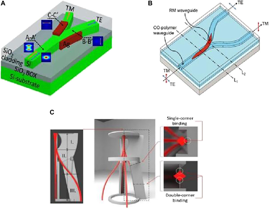
FIGURE 1. Optimal design of y-branch beam splitter. (A) Structural diagram of y-branch polarization beam splitter of hybrid plasma waveguide [35]. (B) Schematic diagram of polarization beam splitter inserted with high birefringence material [36]. (C) Schematic diagram of 3D polymer beam splitting using laser direct writing technology [48]. Figure reproduced with permission from: (A), © 2016, Institute of Electrical and Electronics Engineers (IEEE); (B), © 2017, Nature Portfolio; (C), © 2021, Institute of Electrical and Electronics Engineers (IEEE).
In addition to the traditional strip y-branch waveguide, subwavelength grating (SWG) waveguide, photonic crystal waveguide, surface plasmon polaritions (SPPs) and 3D polymer are also methods to realize y-type splitting. The photonic crystal power splitter [38] can achieve 99.2% of the total transmission efficiency. It mainly uses the plane wave expansion method to study the dispersion characteristics between guided modes in the photonic band gap. The ultra-wide band y splitter based on planar terahertz plasma metamaterials [42] has similar dispersion relationships and mode characteristics with SPPs. As for the 3D polymer beam splitting using laser direct writing technology [48–51], we can also see the performance of y-branch (Figure 1C). However, a challenge is that due to technical limitations, the traditional y-branch single-mode waveguide is difficult to measure, and can only be made into multi-mode waveguide for experiments [49]. Since SWG can increase the degree of freedom of waveguide design, effectively reduce the footprint of waveguide devices, and realize the low loss coupling between single-mode fiber and waveguide. It can not only be applied to design the beam splitting structure, but also introduce delay characteristics into beam splitting. It is often used in the design of waveguide devices. For the two functions of power beam splitting and polarization beam splitting, Nib combined them with a splitter using SWG and hybrid plasma grating in 2018 [44]. TE mode can be divided, while TM mode is reflected by hybrid plasma grating. By this way, polarization selection and power distribution are realized simultaneously by using a single device. The device is ultracompact, and the transverse size is only 6.2 μm.
As a dominant device in large-scale photonic integration, the cascaded y-branch waveguide [40, 41] can achieve 2n channel uniform output. The y-branch has achieved 1 × 256 [40] splitters, which is of great significance for the efficient utilization of sources and large-scale photonic integrated chips. As a result, the ultralow-loss y-branch splitter is the goal of many researchers at present, which can be used in ultralow-loss photon propogation and optical interconnection. For example, in reference [41], a 1 × 64 cascaded y-branch splitter based on silica-on-silicon material platform for telecommunication applications is proposed. The result confirms very low insertion loss 0f −19.28dB, which is the lowest loss value in cascaded 1 × 64 splitters as far as we know.
The beam splitter based on MMI coupling principle is a more mainstream beam splitting method in recent years. Compared with the above y-branch splitter, it is not limited by the radiation loss of the branch angle, so the transverse size is greatly reduced. According to the general design principle, it can realize multi inputs and multi outputs distribution. In recent years, for different separation characteristics, a number of improved designs for multimode waveguides have emerged, which can efficiently realize the functions of power beam splitting [60–67], polarization beam splitting [52–59], wavelength division multiplexing (WDM) [110–114], mode division multiplexing (MDM) [68, 115, 116], and the power splitter based on MMI coupling is easy to realize polarization-insensitive design. By analyzing the propagation of the photons, it is known that the position of the reproduced n-double image is:
Where
According to the above design principles, different MMI devices can be designed according to functional requirements.
For the polarization beam splitting, the multimode waveguide of MMI coupler is often specially designed to allow only one mode to pass through and the other mode to cut off. It is found that, on the one hand, multimode waveguides can be combined with waveguides of other types or materials to achieve the purpose of polarization beam splitting. For example, Guan combined the MMI coupler with the hybrid plasmonic waveguide [53]. Due to the hybird plasmonic effect, the multimode region covered by the metal strip realized the imaging of the TE polarization mode, while the higher-order TM mode was hardly excited without imaging. The multimode region of the device under this method is only 1.1 μm. Compared with polarization beam splitter based on evanescent field coupling, the length is shorter and the fabrication is simpler. The combination of multimode waveguide region and asymmetric slot multimode silicon waveguide [52] (Figure 2A) is also an effective means to realize polarization separation. TE mode can enter the through port through multimode waveguide, while TM mode forms an image at the cross port. In addition, the compact polarization beam splitter combines silicon waveguides and silicon nitride waveguides [54], and can propogate two polarizations to waveguides of different materials respectively. This method can control two polarization states independently, and has the advantages of low insertion loss, high polarization extinction ratio and width response.
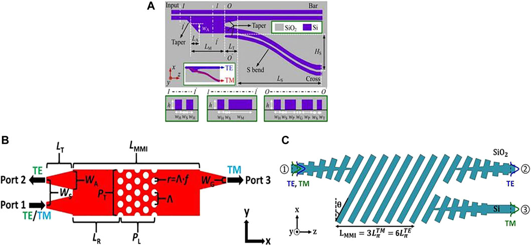
FIGURE 2. MMI coupling structure for polarization beam splitting. (A) MMI polarization beam splitter based on slot waveguide [52]. (B) The photonic crystal structure is etched in the multimode region, and the two polarizations are separated from each other in the opposite direction [57]. (C) The inclined grating structure is used to replace the traditional MMI to realize the independent selection of two orthogonal polarization [59]. Figure reproduced with permission from: (A), © 2014, Institute of Electrical and Electronics Engineers (IEEE); (B), © 2019, Institute of Electrical and Electronics Engineers (IEEE); (C), © 2019, Institute of Electrical and Electronics Engineers (IEEE).
On the other hand, introducing other micro/nano structures into MMI couplers [57, 59] is also an interesting method to realize polarization beam splitting. For example, a photonic crystal structure is introduced in the multimode region (Figure 2B), and different polarizations are reflected and transmitted by optimizing the photonic crystal band-gap structure. Moreover, the introduction of an inclined grating (Figure 2C) on the basis of the MMI coupling structure can achieve accurate control of the structural anisotropy and allow independent selection of the beat length of two orthogonal polarization states. The structure achieves that the insertion loss is less than 1 dB and extinction ratio greater than 20 dB in the broadband range of 131 nm.
Power beam splitting is also an important function of MMI coupler. The classical splitters based on MMI couplers and directional couplers are often sensitive to polarization, so the polarization insensitive power splitter is a research hotspot in recent years. It is found that the polarization insensitivity can be achieved by improving the classical MMI coupler. On the one hand, for an independent MMI coupler, the effective refractive index of TE and TM modes can be changed depending on the special design of multimode structure, so that the coupling intensity of the two modes is equal, so as to realize polarization insensitivity. For the special design of multimode region, there are mainly two methods: introducing SWG and introducing shallow etching region. For example, The SWG with gradual width is etched in the multi-mode region of MMI [60, 61]. The most significant advantage of them is very compact. Among them, the multi-mode region in Figure 3A is only 1.92 μm. Particularly, the structure uses extensible method to convert fundamental mode to higher order modes thus realizing a compact mode order power division converter, with a conversion efficiency of 99% [62]. The shallow etching area is designed in the conical area in front of the output waveguide. In this case, the TM mode is equivalent to output through a y-branch waveguide [64]. For the independent MMI coupler, there is also a polarization independent design, which shifts the focus to the conical region in front of the multimode region (Figure 3B), converts all waveguides into grating waveguides, and uses different gratings to separate the polarization states [67]. However, compared with the above design methods, this method has relatively large loss and is not compact enough.
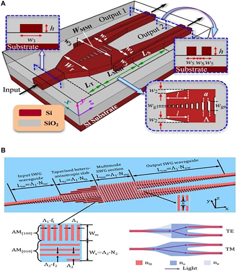
FIGURE 3. MMI coupling structure for power beam splitting. (A) The SWG with variable width is etched in the multimode region, and the output is designed as slot waveguide to realize mode conversion [60]. (B) Introducing conical grating structure in front of multimode region [67]. Figure reproduced with permission from: (A), © 2015, Institute of Electrical and Electronics Engineers (IEEE); (B), © 2021, Institute of Electrical and Electronics Engineers (IEEE).
On the other hand, the cascaded MMI coupler [63] can also be used in polarization independent design, where phase shifter is introduced between a 1×N and a N×N MMI couplers, and the same power output with different polarizations can be achieved by optimizing the length of the phase shifter. Similar structures can also be applied to multi-channel optical switches and multi-channel optical modulation.
MMI couplers are also suitable for designing WDM and MDM. To realize this function, several MMI couplers need to be cascaded or a single MMI coupler needs to be specially designed. Two 3 × 3 MMI, and three phase shifters are introduced. The input fundamental mode, first-order mode and second-order mode can be converted into fundamental mode output at the same time to realize mode demultiplexing [115]. The same design idea can also be applied to WDM. Two cascaded 4 × 4 MMI couplers [112] (Figure 4A), or three cascaded 1 × 2 MMI couplers [113] (Figure 4B) can realize the four channel WDM, increasing the number of input and output ports of the MMI coupler, maintaining the best power separation characteristics, and expanding the performance of the device to support multiple channels. In recent years, an independent angle MMI [114] for WDM has been proposed. It has the advantages of simple design and compatible manufacturing process. Since the processing temperature is less than 400°C, a multi-layer integration scheme can be realized. By combining a single MMI coupler with a y-branch waveguide [116], mode conversion and multiplexing can be realized. Due to the introduction of sub wavelength gratings (Figure 4C), this paves the way for further improving the transmission and bandwidth capacity of photon interconnection.
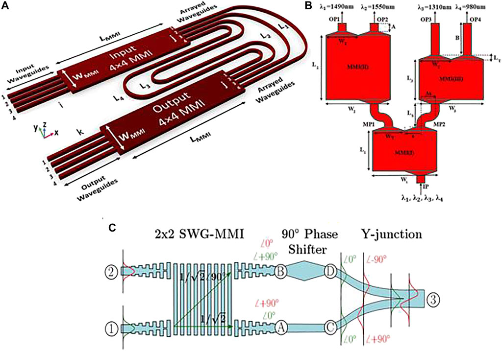
FIGURE 4. MMI coupling structure for WDM and MDM. (A) Two 4 × 4 MMIs are cascaded for WDM [112]. (B) Three 1 × 2 MMIs are cascaded for WDM [113]. (C) MMI based on SWG is combined with y-branch to realize mode conversion and multiplexing [116]. Figure reproduced with permission from: (A), © 2021, Institute of Electrical and Electronics Engineers (IEEE); (B), © 2021, Springer; (C), © 2018, Institute of Electrical and Electronics Engineers (IEEE).
Similar to the above two structures, DC is often used for power and polarization separation, and it is also an important part of other integrated optoelectronic devices such as MZI and microcavity. Here we divide directional couplers into symmetric and asymmetric structures to discuss their research progresses.
The common symmetrical DC has a simple structure, which is composed of two parallel straight waveguides or two longitudinally symmetrical curved waveguides. It works by mode coupling with waveguides in the middle. It is often used as a 3 dB power beam splitter and combiner, such as the beam splitting and combiner of MZI. By changing it without changing its symmetry, polarization beam splitting and multi-channel power beam splitting can be realized. For example, adding a silicon waveguide for bridging between two parallel waveguides [117] can realize the separation of polarization states, and the polarization extinction ratio of TE mode and TM mode can reach about 40 dB. The introduction of subwavelength grating structure into symmetrical directional coupler [118] is an effective method to realize polarization independent power beam splitting. As shown in Figure 5A, subwavelength gratings are etched on both sides of the intermediate input waveguide and the inner side of the output waveguide. The effect is to enhance the coupling strength of one polarization state and have little effect on the other polarization state, so that the coupling lengths of the two modes are equal. Recently, a similar coupling method has been used in the reference [119]. The difference is that the central input waveguide uses a strip waveguide combined with a hybrid plasma waveguide, and the power splitter is only designed for TE mode, achieving an insertion loss of 0.56 dB and an extinction ratio of 23.74 dB. To realize multi-channel power beam splitting, it can be combined with slot waveguide to determine the coupling length and waveguide gap, so as to realize four-channel power output [73]. However, compared with the multi-channel power splitter using MMI coupler, this method requires a larger footprint.
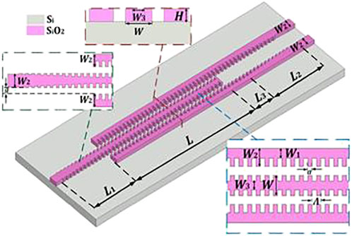
FIGURE 5. Optimal design of symmetrical DC. DC with bridged silicon waveguide etched with subwavelength grating [118]. Figure reproduced with permission from: © 2020, Elsevier.
In recent years, asymmetric DC have more abundant research results. They can design beam splitting devices more flexibly to achieve more compact area and better performance. Asymmetric DC designed for polarization beam splitting are particularly abundant. Here, the design ideas of asymmetric DC are roughly divided into the following categories: the first is to introduce a SWG structure into the traditional DC, including the grating as a bridge waveguide [120], and etching the SWG on the strip waveguide at both ends of the coupler [121–123]. Among them, a representative work is proposed in reference [124], two SWG waveguides are applied in 2 × 2 adiabatic 3 dB coupler, which support two transverse electric modes and achieve an adiabatic mode evolution of the two-waveguide system for broadband 3 dB power splitting with 130 nm wavelength range. This is similar to the reason why symmetrical directional couplers introduce gratings. The scattering characteristics of subwavelength gratings provide more flexible design degrees of freedom for the design of polarization beam splitters, which can often enhance the coupling strength of one polarization mode without affecting the other polarization. The second is to make several different types of waveguide structures work together, so as to achieve the effect that a single waveguide type is difficult to achieve. At present, the existing combination forms include the combination of GaAs nanowires and hybrid plasma waveguides [125], the combination of silicon nanowires and nanobelt waveguides [70] (Figure 6A), and the combination of slot waveguides and waveguides embedded with gratings [126]. The third common design scheme is the curved directional coupler [71, 127–130]. For example, conical curved waveguide is introduced into the curved DC part, which enhances the coupling strength and significantly shortens the coupling length, so that higher coupling and conversion efficiency can be obtained in a wide bandwidth with a small footprint [129]. This idea is also applicable to polarization beam splitting and mode multiplexing. Another bent DC used in a thermo-optic switch is proposed to replace the multimode interferometers or straight DCs, so that achieves a coupling ratio of 50%:50%, as well as low excess loss over a broadband.
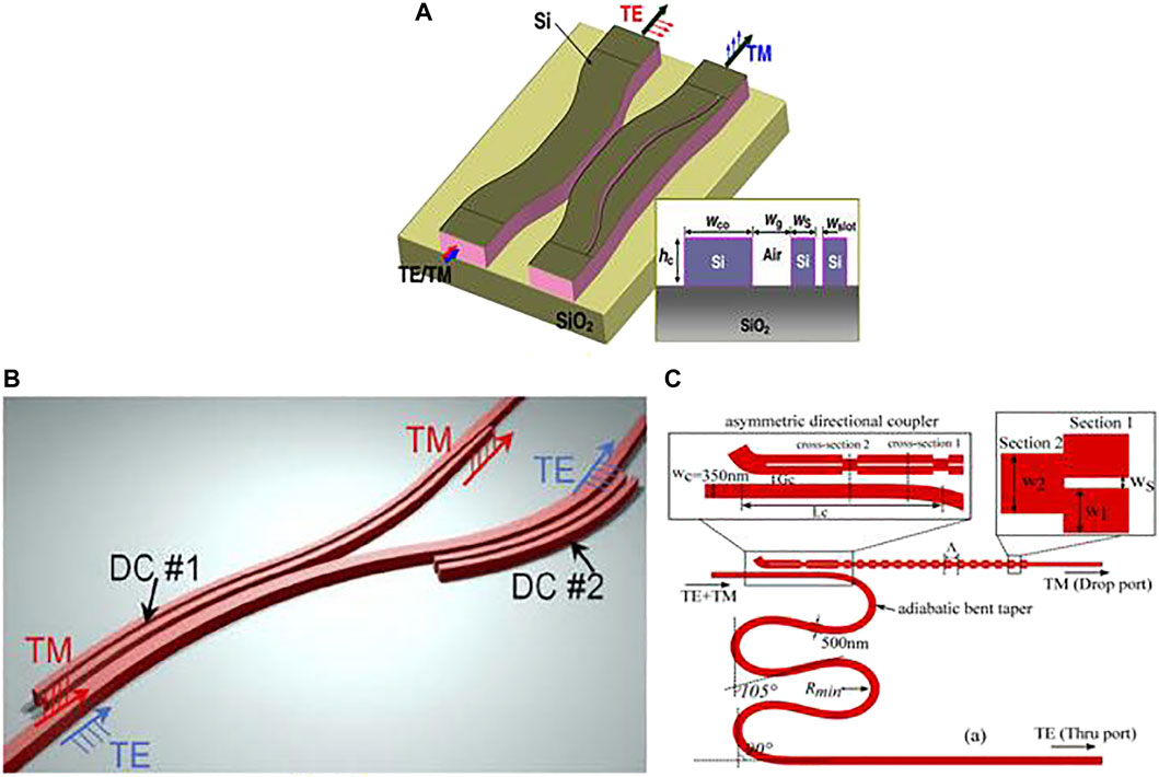
FIGURE 6. Optimal design of asymmetric DC. (A) DC composed of different types of waveguides [70]. (B) Cascaded DC for polarization beam splitting [127]. (C) Polarization splitter with periodic etched structure and curved waveguide [131]. Figure reproduced with permission from: (A), © 2011, Optical Society of America (OSA); (B), © 2021, Optical Society of America (OSA); (C), © 2020, Optical Society of America (OSA).
In addition, as shown in Figure 6B, by combining the similar curved waveguides with the slot waveguide, the TE extinction ratio is greater than 30dB, which is the first high-performance silicon-based splitter operating in the 2 μm band [127]. In addition to the above three common design ideas, in recent years, a polarization beam splitter with etched periodic structure and curved waveguide has been proposed [131], with extinction ratio of 36 dB for TE polarization. The advantage is that more periodic structures and curved waveguides are used (Figure 6C), and the polarization extinction ratio can continue to improve without significantly affecting the insertion loss of the output port.
These results will have great application value in the field of optical interconnection and optical communication. As the beam splitting part of integrated devices, they have great development potential in large-scale quantum chips.
Different from the above three traditional design methods of micro nano structures, the methods using concept of inverse design often deduces the corresponding structural parameters from the performance indicators of devices, which can not only realize the optimal design of devices, but also use programmable methods to design silicon-based optoelectronic devices with adjustable functions. At present, there are inverse design splitters based on a variety of optimization algorithms, such as direct binary search algorithm, topology optimization, gradient descent optimization algorithm, and combination of topology constraints and direct binary search algorithm. In 2015, Shen used the direct binary search algorithm (DBS) [76] to iteratively calculate the pixel states in the beam splitting structure step by step. This method uses the concept of free-form metamaterials in the polarization beam splitter, allowing the geometric structure of metamaterials to be optimized, making the device very compact. It is experimentally proved that an average transmission efficiency of greater than 70% and an extinction ration greater than 10 dB within a bandwidth of 32 nm are realized. As for the fabrication, a single lithography step is enough for the fabrication of the splitter and input/output waveguides and the device is tolerant to fabrication errors up to ±20 nm in the device thickness. However, its transmittance does not reach the level of the traditional beam splitter. Therefore, to ensure the excellent transmission performance of the device and to realize the compact and flexible design of the structure is the forward direction of the splitter based on inverse design. Compared with introducing multiple etch points in multimode structure, changing the edge shape of the splitter by using topology optimization is an effective method to realize compact power beam splitter. As shown in Figure 7A, it uses topology optimization and gradient descent optimization algorithms to achieve uniform three-way power output [77]. It is worth noting that the splitter is designed directly incorporates fabrication constraints and the device have no small features which would be difficult to resolve with photolithography. The splitter has a insertion loss of 0.642 ± 0.057 dB and power uniformity of 0.641 ± 0.054 dB. In addition to the above two schemes, in 2018, Chang proposed to combine topological constraints and nonlinear direct binary search algorithm [78] to realize a dual-mode 3 dB power splitter (Figure 7B). In this paper, Matlab is also used to randomly generate different initial mode distributions, select multiple device sizes, and then perform iterative calculation one by one, so as to select the structure size with the best performance, making the whole device more reliable. Finally, the footprint is only 2.88 μm×2.88 μm. The crosstalk of both modes is less than −20 dB within the bandwidth of 60 nm. It is found that the device is also robust to fabrication errors.
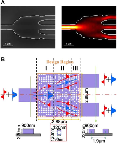
FIGURE 7. Design of beam splitter based on inverse design. (A) Simulation diagram of power splitter based on topology optimization algorithm [77]. (B) Dual mode power splitter based on nonlinear DBS algorithm and topology optimization [78]. Figure reproduced with permission from: (A), © 2017, Conference on Lasers and Electro-Optics (CLEO); (B), © 2018, Optical Society of America (OSA).
Adjoint method is a technique that allows the gradient of an objective function to be computed with respect to an arbitrarily large number of degrees of freedom using only two full-field simulations [132]. In the reference [79], the inverse design problem thus reduces to finding the permittivity and electric fields which simultaneously satisfy physics and the device performance constraints. Compared with other methods, the adjoint methods are more suitable for gradient-based design of electromagnetic structures with respect to a large number of free parameters. Meanwhile, it can be generalized to nonlinear optical devices to create new possibilities.
Generally speaking, Due to the increase of design freedom and the use of various optimization algorithms, the footprint of inverse design splitters is compact, which is two orders of magnitude smaller than that of conventional one. However, insertion loss, extinction ratio and other parameters have no obvious advantages compared with that of traditional design methods. The complexity of inverse design splitters mainly depends on the complexity of algorithm, which is also closely related to our requirements for performance and function. As for the fabrication, the processing of inverse design splitters mainly depends on lithography and is compatible with CMOS process and shows the robustness to manufacturing tolerance, which requires that the processing constraints be considered in the design.
In general, as one of the most basic on-chip passive devices, optical beam splitter is an important part of a variety of on-chip active and passive devices and systems. Different beam splitting methods can split light waves from multiple angles and dimensions. The ultracompact integrated optical system, cutting-edge optoelectronic integration technology and large-scale quantum chip may contain hundreds of active and passive devices, which are closely linked and work together to realize the specific functions of the entire optical chip. Therefore, the applications of on-chip beam splitters are discussed from three aspects: related integrated optical devices, large-scale quantum chips and optoelectronic hybrid integrated chips.
Integrated optical devices including splitters mainly include optical interferometer [133–138], optical coupler [139–141], optical modulator [82–98], optical switch [142], optical router [143], mixer [144], optical isolator [145]. They play different roles in wavelength division multiplexing, time division multiplexing, space division multiplexing and other multiplexing systems, so as to meet the growing demand for communication capacity. Taking the optical modulator and optical switch as an example, the beam splitting structure is often combined with the MZI, and the signal is modulated through the refractive index phase difference of different beam splitting channels through electro-optic, thermo-optic, acousto-optic and other effects. For example, the Y-branch is used to split or combine the thermo-optic MZI [146], with an extinction ratio of −16.5 dB, a rise time of 10 μs and a descent time of 20μs. The power consumption of π phase shift is 0.39w. The micro ring structure with directional coupling beam splitter can be used not only for optical modulation, but also for micro ring filter [147] and micro ring switch array. As for the optical coupler, in the DAS underwater communication system proposed in recent years [139], it is convenient to use the optical coupler to divide the source into two. One beam of light is modulated by the acousto-optic modulator to generate the probe optical pulse with the frequency offset of MHz. The implementation of optical router cannot be separated from the participation of beam splitter. In the paper [143], Chen Kaixuan proposed using 3 dB splitter and optical switch to simultaneously control and route multiple modes, which is of great significance in simplifying network system routing, sharing switch resources, reducing power consumption and reducing size. As early as 2007, Tao Dongjie used the splitter based on MMI to realize the compact and easy to integrate optical isolator for TM mode isolation [145]. It can be seen that a large part of integrated optical devices are inseparable from the beam splitting structure. They are often connected to each other and become an important part of the optical system on chip.
In recent years, large-scale quantum chips, quantum propogation and manipulation in large-scale integrated optical paths have become a frontier research hotspot. On the one hand, from the research fields of quantum state preparation and quantum theory, the splitter can play a role in the following three aspects [148]. First, the beam splitter can participate in the preparation of quantum entanglement sources. For example, the symmetric splitter can prepare EPR quantum entangled states [149]; Second, the splitter can participate in the quantum operation generated by optical transformation, mainly including complex fractional Fourier transform, entangled fractional Fourier transform, and the operation of increasing and decreasing photons [150]; Third, the splitter can be used to simulate quantum dissipation in combination with conditional measurement. For example, the input is in vacuum state and the amplitude attenuation channel is simulated [151]. On the other hand, from the research of large-scale integrated optical quantum chips in recent years, the beam splitter is an indispensable part. For example, in the new on-chip high-dimensional quantum state preparation and regulation method [152] published by Wang on Science in 2018, 122 MMI beam splitters and MZIs with unequal arm lengths are used for 16 on-chip single photon wavelength division multiplexing, realizing the loading of multi-path information, so that each photon exists in multiple optical waveguides in the form of superposition of quantum states, with strong correlation and entanglement, up to 15 × 15. This research result is of great significance for high-precision, programmable, arbitrary general-purpose quantum manipulation and quantum measurement of high-dimensional quantum entangled systems. In addition, the research team of Peking University also showed the importance of the splitter in the generalized multipath delay selection experiment [153] of large-scale quantum nano photonic chips published in 2021. As shown in Figure 8B, the state of the d-mode quantum controlled splitter determines the delay selection. The multimode quantum system thus constructed provides a multi-functional platform for the study of multimode quantum superposition and coherence, and also provides in-depth insights into the benchmark controllability of multi-dimensional quantum physics and integrated optical quantum technology.
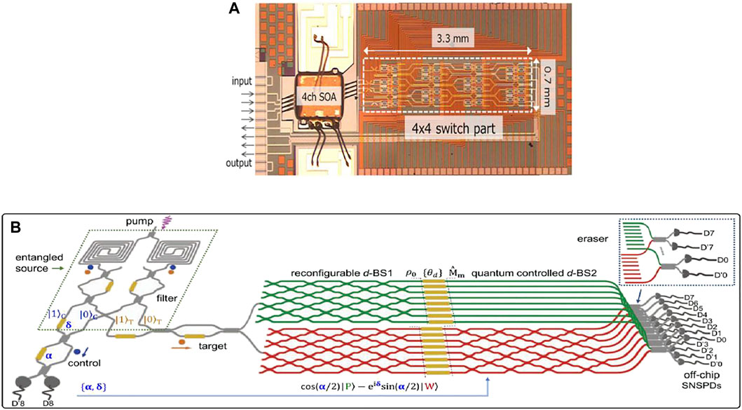
FIGURE 8. Application of splitter in large scale quantum chip and optoelectronic hybrid integration. (A) The microscope image of fabricated 4 × 4 Si switch with hybrid-integrated InP-SOA [154]. (B) Generalized multipath delay selection for large scale quantum nano photonic chips [153]. Figure reproduced with permission from: (A), © 2018, Institute of Electrical and Electronics Engineers (IEEE); (B), © 2021, Nature Portfolio.
In addition, the beam splitter also plays an irreplaceable role in optoelectronic hybrid integration. The current optoelectronic hybrid integration scheme is to integrate electronic devices and photonic devices on the same silicon chip. The splitter used to connect silicon-based lasers and many photonic devices undertakes the important tasks of optical wavelength multiplexing/demultiplexing, optical wavelength tuning and conversion. For example, in the hybrid integration of flip chip based semiconductor optical amplifiers (SOA) on a silicon photonics platform [154], it can be seen from the microscope image of fabricated 4 × 4 Si switch with hybrid-integrated InP-SOA (Figure 8A), whether it is between the SOA and the multi-channel optical waveguide of the front input or between the SOA and the rear 4 × 4 switch part, even the switch array are full of beam splitters. As a result, the large compact silicon optical matrix switch has become the key part of the optical path network, and the loss and size of the splitter also greatly affect the lossless propogation of the entire optical path network.
In conclusion, the on-chip beam splitting methods in recent years are summarized and reviewed. Firstly, the basic principles of four beam splitting methods are introduced; Secondly, the design methods of beam splitter based on y-branch, MMI coupling, DC and inverse design algorithm are introduced. Through the comparison of these beam splitting methods, it is found that the structural design of each beam splitting method is diverse, but there are many common points in the design ideas, including the introduction of sub wavelength grating into the traditional structure, Traditional silicon waveguides can be combined with waveguides of other types or materials, or other waveguides can be directly used to achieve similar functions. Through this review, the future research directions for beam splitting methods are clarified, that is, increasing transmittance, reducing loss, improving extinction ratio, reducing volume, etc., and the flexibility of device design should be continuously enhanced. Finally, this paper also discusses the applications of the on-chip beam splitting method. Although the on-chip beam splitter is a basic unit in the integrated optical circuit, it plays an important role in many positions of the on-chip optical circuit. Whether now or in the future, the splitter is very important for the cutting-edge large-scale quantum chips, high-speed quantum bit propogation, optoelectronic hybrid integration and other fields.
YX, ZT, XM, and ZC contributed to the writing of the review, everyone was involved in the drafting and critical revision of the manuscript. YX was responsible for writing the main contents of the manuscript. ZT and XM were responsible for searching and sorting out the data of “Application of beam splitter”. ZC was responsible for providing ideas for the overall structure of the article.
The authors declare that the research was conducted in the absence of any commercial or financial relationships that could be construed as a potential conflict of interest.
All claims expressed in this article are solely those of the authors and do not necessarily represent those of their affiliated organizations, or those of the publisher, the editors and the reviewers. Any product that may be evaluated in this article, or claim that may be made by its manufacturer, is not guaranteed or endorsed by the publisher.
1. Liu YA, Yan XS, Wu JW, Zhu B, Chen Y, Chen X. On-chip erbium-doped lithium niobate microcavity laser. Sci China Phys Mech Astron (2021) 64(3):234262–5. doi:10.1007/s11433-020-1625-9
2. Kharas D, Plant J, Bramhavar S, Loh W, Swint R, Sorace-Agaskar C, et al. High power (> 300 mW) 1550 nm on-chip laser realized using passively aligned hybrid integration. In: CLEO: Science and Innovations. 10-15 May 2020, San Jose, CA, USA, Optical Society of America (2020). STu3M. 3.
3. Grassani D, Tagkoudi E, Guo H, Herkommer C, Yang F, Kippenberg TJ, et al. Mid infrared gas spectroscopy using efficient fiber laser driven photonic chip-based supercontinuum. Nat Commun (2019) 10(1):1553–8. doi:10.1038/s41467-019-09590-3
4. Hughes TW, Tan S, Zhao Z, Sapra NV, Leedle KJ, Deng H, et al. On-chip laser-power delivery system for dielectric laser accelerators. Phys Rev Appl (2018) 9(5):054017. doi:10.1103/physrevapplied.9.054017
5. Dabos G, Manolis A, Giesecke AL, Porschatis C, Chmielak B, Wahlbrink T, et al. TM grating coupler on low-loss LPCVD based Si3N4 waveguide platform. Opt Commun (2017) 405:35–8. doi:10.1016/j.optcom.2017.07.088
6. Han X, Jiang Y, Frigg A, Xiao H, Zhang P, Boes A, et al. Single-step etched grating couplers for silicon nitride loaded lithium niobate on insulator platform. APL Photon (2021) 6(8):086108. doi:10.1063/5.0055213
7. Ghannam I, Merget F, Witzens J. Silicon nitride C-band grating couplers with reduced waveguide back-reflection. In: Optical Interconnects XXII; 2022 March 5; San Francisco, CA. SPIE (2022). p. 155–61. 12007.
8. Fatkhiev DM, Lyubopytov VS, Kutluyarov RV, Grakhova EP, Sultanov AK. A grating coupler design for optical vortex mode generation in rectangular waveguides. IEEE Photon J (2021) 13(4):1–8. doi:10.1109/jphot.2021.3089664
9. Liu M, Chen D, Hu X, Feng P, Xiao X. Efficient silicon nitride grating coupler with silicon reflector at near-infrared wavelengths. In: Asia Communications and Photonics Conference. Optical Society of America, 24-27, Oct. 2020, Beijing, China. M4A. 166.
10. Molina-Fernández I, Halir R, Ortega-Moñux A, Wangüemert-Pérez JG, Chen Y, He JJ, et al. Broadband and high-performance devices for the silicon and silicon-nitride platforms. In: 2017 19th International Conference on Transparent Optical Networks (ICTON). IEEE 02-06 July 2017, Girona, Spain. p. 1–4.
11. Cheng L, Mao S, Mu X, Wu S, Fu HY, Dual-wavelength-band multiplexed grating coupler on multilayer SiN-on-SOI photonic integrated platform. In: CLEO: QELS_Fundamental Science. Optical Society of America 10-15 May 2020, San Jose, CA, USA. JTh2F. 8.
12. Yang F, Fang H, Han H, Xiang B. Wide bandwidth silicon nitride strip-loaded grating coupler on lithium niobate thin film. Crystals (Basel) (2022) 12(1):70. doi:10.3390/cryst12010070
13. Dwivedi S, Song B, Liu Y, Moreira R, Johanson L, Klamkin J, et al. Demonstration of compact silicon nitride grating coupler arrays for fan-out of multicore fibers. In: 2017 Conference on Lasers and Electro-Optics (CLEO). IEEE 14-19 May 2017, San Jose, CA, USA. p. 1–2.
14. Song JH, Snyder B, Lodewijks K, Jansen R, Rottenberg X. Grating coupler design for reduced back-reflections. IEEE Photon Technol Lett (2017) 30(2):217–20. doi:10.1109/lpt.2017.2783759
15. Nambiar S, Kumar A, Kallega R, Ranganath P, Selvaraja SK. High-efficiency grating coupler in 400 nm and 500 nm PECVD silicon nitride with bottom reflector. IEEE Photon J (2019) 11(5):1–13. doi:10.1109/jphot.2019.2936430
16. Sapra NV, Vercruysse D, Su L, Yang KY, Skarda J, Piggott AY, et al. Inverse design and demonstration of broadband grating couplers. IEEE J Sel Top Quan Electron (2019) 25(3):1–7. doi:10.1109/jstqe.2019.2891402
17. Kohli M, Messner A, Buriakova T. Highly efficient grating coupler for silicon nitride photonics with large fabrication tolerance. In: Integrated Photonics Research, Silicon and Nanophotonics; 2021 July 26–29; Washington, DC. Optical Society of America (2021). IM4A. 6.
18. Mak JCC, Wilmart Q, Olivier S, Menezo S, Poon JKS. Silicon nitride-on-silicon bi-layer grating couplers designed by a global optimization method. Opt Express (2018) 26(10):13656–65. doi:10.1364/oe.26.013656
19. Zhang Z, Shan X, Huang B, Cheng C, Bai B, Gao T., et al. Efficiency enhanced grating coupler for perfectly vertical fiber-to-chip coupling. Materials (2020) 13(12):2681. doi:10.3390/ma13122681
20. Cheng L, Mao S, Li Z, Han Y, Fu H. Grating couplers on silicon photonics: Design principles, emerging trends and practical issues. Micromachines (2020) 11(7):666. doi:10.3390/mi11070666
21. Zhu Y, Wang J, Xie W, Tian B, Li Y, Brainis E, et al. Ultra-compact silicon nitride grating coupler for microscopy systems. Opt Express (2017) 25(26):33297–304. doi:10.1364/oe.25.033297
22. Su L, Trivedi R, Sapra NV, Piggott AY, Vercruysse D, Vuckovic J. Fully-automated optimization of grating couplers. Opt Express (2018) 26(4):4023–34. doi:10.1364/oe.26.004023
23. Jian J, Xu P, Chen H, He M, Wu Z, Zhou L, et al. High-efficiency hybrid amorphous silicon grating couplers for sub-micron-sized lithium niobate waveguides. Opt Express (2018) 26(23):29651–8. doi:10.1364/oe.26.029651
24. Mak JCC, Sacher WD, Ying H, Luo X, Lo PGQ, Poon JKS. Multi-layer silicon nitride-on-silicon polarization-independent grating couplers. Opt Express (2018) 26(23):30623–33. doi:10.1364/oe.26.030623
25. Sacher WD, Luo X, Yang Y, Chen FD, Lordello T, Mak JCC, et al. Visible-light silicon nitride waveguide devices and implantable neurophotonic probes on thinned 200 mm silicon wafers. Opt Express (2019) 27(26):37400–18. doi:10.1364/oe.27.037400
26. Mak JCC, Wilmart Q, Olivier S, Menezo S, Poon JKS. Optimization design of efficient broadband bi-layer grating couplers for a silicon nitride-on-silicon foundry platform. In: Optical Fiber Communication Conference. Optical Society of America 11-15 March 2018, San Diego, CA, USA. Tu2A. 5.
27. Xu P, Zhang Y, Shao Z, Liu L, Zhou L, Yang C, et al. High-efficiency wideband SiNx-on-SOI grating coupler with low fabrication complexity. Opt Lett (2017) 42(17):3391–4. doi:10.1364/ol.42.003391
28. Liu Y, Huang X, Li Z, Guan H, Wei Q, Fan Z, et al. Efficient grating couplers on a thin film lithium niobate–silicon rich nitride hybrid platform. Opt Lett (2020) 45(24):6847–50. doi:10.1364/ol.413246
29. Nambiar S, Muthuganesan H, Sharma T, Selvaraja SK. On-chip unidirectional dual-band fiber-chip grating coupler in silicon nitride. OSA Continuum (2018) 1(3):864–71. doi:10.1364/osac.1.000864
30. Song JH, Kongnyuy TD, Troia B, Saseendran SS, Soussan P, Jansen R, et al. Grating devices on a silicon nitride technology platform for visible light applications. OSA Continuum (2019) 2(4):1155–65. doi:10.1364/osac.2.001155
31. Hong J, Spring AM, Qiu F, Yokoyama S. A high efficiency silicon nitride waveguide grating coupler with a multilayer bottom reflector. Sci Rep (2019) 9(1):12988–8. doi:10.1038/s41598-019-49324-5
32. Nambiar S, Ranganath P, Kallega R, Selvaraja SK. High efficiency DBR assisted grating chirp generators for silicon nitride fiber-chip coupling. Sci Rep (2019) 9(1):18821–9. doi:10.1038/s41598-019-55140-8
33. Wang X, Quan X, Liu M, Cheng X. Silicon-nitride-Assisted edge coupler interfacing with high numerical aperture fiber. IEEE Photon Technol Lett (2019) 31(5):349–52. doi:10.1109/lpt.2019.2895095
34. Hoppe N, Zaoui WS, Rathgeber L, Wang Y, Klenk RH, Vogel W, et al. Ultra-efficient silicon-on-insulator grating couplers with backside metal mirrors. IEEE J Sel Top Quan Electron (2019) 26(2):1–6. doi:10.1109/jstqe.2019.2935296
35. Hu T, Qiu H, Zhang Z, Guo X, Liu C, Rouifed M, et al. A compact ultrabroadband polarization beam splitter utilizing a hybrid plasmonic Y-branch. IEEE Photon J (2016) 8(4):1–9. doi:10.1109/jphot.2016.2585113
36. Huang G, Park TH, Oh MC. Broadband integrated optic polarization splitters by incorporating polarization mode extracting waveguide. Sci Rep (2017) 7(1):4789–7. doi:10.1038/s41598-017-05324-x
37. Sun C, Zhao J, Wang Z, Du L, Huang W. Broadband and high uniformity Y junction optical beam splitter with multimode tapered branch. Optik (2019) 180:866–72. doi:10.1016/j.ijleo.2018.12.013
38. Singh S, Singh K. Design of an integrated multi-arm power splitter using photonic crystal waveguide. Optik (2017) 145:495–502. doi:10.1016/j.ijleo.2017.08.021
39. Danaie M, Nasiri Far R, Dideban A. Design of a high-bandwidth Y-shaped photonic crystal power splitter for TE modes. Int J Opt Photon (2018) 12(1):33–42. Y型光子晶体功分器. doi:10.29252/ijop.12.1.33
40. Wang L, Sun B, Zhang J, An J, Li J, Yin X, et al. Low-loss 1 × 256 optical power splitter. Opt Eng (2021) 60(12):127102. doi:10.1117/1.oe.60.12.127102
41. Serečunová S, Seyringer D, Seyringer H, Uherek F. Design and optimization of 1 × 2 N Y-branch optical splitters for telecommunication applications. J Electr Eng (2020) 71(5):353–8. doi:10.2478/jee-2020-0048
42. Gao X, Zhou L, Yu XY, Cao WP, Li HO, Ma HF, et al. Ultra-wideband surface plasmonic Y-splitter. Opt Express (2015) 23(18):23270–7. doi:10.1364/oe.23.023270
43. Han L, Kuo BPP, Alic N, Radic S. Ultra-broadband multimode 3dB optical power splitter using an adiabatic coupler and a Y-branch. Opt Express (2018) 26(11):14800–9. doi:10.1364/oe.26.014800
44. Ni B, Xiao J. Ultracompact and broadband silicon-based TE-pass 1 × 2 power splitter using subwavelength grating couplers and hybrid plasmonic gratings. Opt Express (2018) 26(26):33942–55. doi:10.1364/oe.26.033942
45. Lin Z, Shi W. Broadband, low-loss silicon photonic Y-junction with an arbitrary power splitting ratio. Opt Express (2019) 27(10):14338–43. doi:10.1364/oe.27.014338
46. Nair DP, Ménard M. A compact low-loss broadband polarization independent silicon 50/50 splitter. IEEE Photon J (2021) 13(4):1–7. doi:10.1109/jphot.2021.3091539
47. Zhang Y, Hu X, Chen D, Wang L, Li M, Feng P, et al. Ultra-broadband, low loss and ultra-compact 3dB power splitter based on Y-branch with step waveguide. In: 2019 24th OptoElectronics and Communications Conference (OECC) and 2019 International Conference on Photonics in Switching and Computing (PSC), IEEE (07-11 July 2019, Fukuoka, Japan. p. 1–3.
48. Gašo P, Pudiš D, Seyringer D, Kuzma A, Gajdosova L, Mizera T, et al. 3D polymer based 1x4 beam splitter. J Lightwave Technol (2020) 39(1):154–61. doi:10.1109/jlt.2020.3026170
49. Seyringer D, Gajdošova L, Gašo P, Jandura D, Pudis D, Experimental verification of 3D polymer based 1x4 Y-branch splitter. In: Nano-, Bio-, Info-Tech Sensors, and 3D Systems IV; 2020 April 22. International Society for Optics and Photonics (2020). p. 1137811.
50. Tao Q, Lu B, Zhai Z, Cheng J, Liu D. Manufacturing a 1 × 16 air-cladding polymeric optical splitter for electro-optical printed circuit boards by femtosecond laser. Opt Eng (2020) 59(1):1. doi:10.1117/1.oe.59.1.017105
51. Moughames J, Porte X, Larger L, Jacquot M, Kadic M, Brunner D. 3D printed multimode-splitters for photonic interconnects. Opt Mater Express (2020) 10(11):2952–61. doi:10.1364/ome.402974
52. Xu Y, Xiao J, Sun X. Compact polarization beam splitter for silicon-based slot waveguides using an asymmetrical multimode waveguide. J Lightwave Technol (2014) 32(24):4282–8. doi:10.1109/jlt.2014.2368583
53. Guan X, Wu H, Shi Y, Dai D. Extremely small polarization beam splitter based on a multimode interference coupler with a silicon hybrid plasmonic waveguide. Opt Lett (2014) 39(2):259–62. doi:10.1364/ol.39.000259
54. Sun X, Alam MZ, Aitchison JS, Mojahedi M. Compact and broadband polarization beam splitter based on a silicon nitride augmented low-index guiding structure. Opt Lett (2016) 41(1):163–6. doi:10.1364/ol.41.000163
55. Chack D, Hassan S, Kumar A. Design and analysis of polarization beam splitter based on cascaded MMI on SOI[C]//Integrated Optics: Devices, Materials, and Technologies XXIV. Int Soc Opt Photon (2020) 11283:1128320.
56. Han L, Liang S, Zhu H, Zhang C, Wang W. A high extinction ratio polarization beam splitter with MMI couplers on InP substrate. IEEE Photon Technol Lett (2015) 27(7):782–5. doi:10.1109/lpt.2015.2392383
57. Xu L, Wang Y, El-Fiky E, Mao D, Kumar A, Xing Z, et al. Compact broadband polarization beam splitter based on multimode interference coupler with internal photonic crystal for the SOI platform. J Lightwave Technol (2019) 37(4):1231–40. doi:10.1109/jlt.2018.2890718
58. Zhan J, Brock J, Veilleux S, Dagenais M. Silicon nitride polarization beam splitter based on polarization-independent MMIs and apodized Bragg gratings. Opt Express (2021) 29(10):14476–85. doi:10.1364/oe.420499
59. Herrero-Bermello A, Luque-González JM, Velasco AV, Ortega-Monux A, Cheben P, Halir R. Design of a broadband polarization splitter based on anisotropy-engineered tilted subwavelength gratings. IEEE Photon J (2019) 11(3):1–8. doi:10.1109/jphot.2019.2912335
60. Xu Y, Xiao J. An ultracompact polarization-insensitive silicon-based strip-to-slot power splitter. IEEE Photon Technol Lett (2015) 28(4):536–9. doi:10.1109/lpt.2015.2502983
61. Zhong W, Xiao J. Ultracompact polarization-insensitive power splitter using subwavelength-grating-based MMI couplers on an SOI platform. Appl Opt (2020) 59(7):1991–7. doi:10.1364/ao.382097
62. Guo Z, Xiao J. Ultracompact mode-order converting power splitter for mid-infrared wavelengths using an MMI coupler embedded with oblique subwavelength grating wires. Opt Commun (2021) 488:126850. doi:10.1016/j.optcom.2021.126850
63. Hassan S, Chack D. Design and analysis of polarization independent MMI based power splitter for PICs. Microelectronics J (2020) 104:104887. doi:10.1016/j.mejo.2020.104887
64. Chen Y, Xiao J. Ultracompact and broadband silicon-based polarization-independent 1 × 2 power splitter using a shallowly etched multimode interference coupler. J Opt Soc Am B (2021) 38(10):3064–70. doi:10.1364/josab.428649
65. Nikolaevsky L, Shchori T, Malka D. Modeling a $1 \times 8$ MMI green light power splitter based on gallium-nitride slot waveguide structure. IEEE Photon Technol Lett (2018) 30(8):720–3. doi:10.1109/lpt.2018.2814639
66. Roggero UFS, Hernández-Figueroa HE. Polymeric power splitters for multiplexing optical biosensors. Opt Laser Technol (2020) 127:106127. doi:10.1016/j.optlastec.2020.106127
67. Han S, Liu W, Shi Y. Ultra-broadband dual-polarization power splitter based on silicon subwavelength gratings. IEEE Photon Technol Lett (2021) 33(15):765–8. doi:10.1109/lpt.2021.3095257
68. Hussain ZL, Fyath RS. Design and simulation of 4-mode (de)multiplexers implemented in conventional and subwavelength grating Si/SiO2 platforms. Optik (2022) 251:168449. doi:10.1016/j.ijleo.2021.168449
69. Mizera T, Pudiš D, Kuzma A, Seyringer D, Gaso P, Micek P, et al. 3D optical splitter based on MMI. Transportation Res Proced (2021) 55:949–54. doi:10.1016/j.trpro.2021.07.181
70. Dai D, Wang Z, Bowers JE. Ultrashort broadband polarization beam splitter based on an asymmetrical directional coupler. Opt Lett (2011) 36(13):2590–2. doi:10.1364/ol.36.002590
71. Wu H, Dai D. High-performance polarizing beam splitters based on cascaded bent directional couplers. IEEE Photon Technol Lett (2017) 29(5):474–7. doi:10.1109/lpt.2017.2657539
72. Kim DW, Lee MH, Kim Y, Kim KH. Planar-type polarization beam splitter based on a bridged silicon waveguide coupler. Opt Express (2015) 23(2):998–1004. doi:10.1364/oe.23.000998
73. Ali BM, Kumar RAN, Khonina SN. A compact design of a balanced 1× 4 optical power splitter based on silicon on insulator slot waveguides. Kompʹut Opt (2018) 42(2):244–7. doi:10.18287/2412-6179-2018-42-2-244-247
74. Zhang Y, Hu X, Chen D, Wang L, Feng P, Li M, et al. Ultra-broadband 3dB power splitter based on silicon slot waveguide. In: CLEO: Applications and Technology. San Jose, CA: Optical Society of America (2018). JW2A. 8.
75. González-Andrade D, Lafforgue C, Durán-Valdeiglesias E, Le RX, Berciano M, Casson E, et al. Polarization-and wavelength-agnostic nanophotonic beam splitter. Scientific Rep (2019) 9(1):1–9. doi:10.1038/s41598-019-40497-7
76. Shen B, Wang P, Polson R, Menon R. An integrated-nanophotonics polarization beamsplitter with 2.4 × 2.4 μm2 footprint. Nat Photon (2015) 9(6):378–82. doi:10.1038/nphoton.2015.80
77. Piggott AY, Petykiewicz J, Su L, Vuckovic J. Fabrication-constrained nanophotonic inverse design. Sci Rep (2017) 7(1):1786–7. doi:10.1038/s41598-017-01939-2
78. Chang W, Ren X, Ao Y, Lu L, Cheng M, Deng L, et al. Inverse design and demonstration of an ultracompact broadband dual-mode 3 dB power splitter. Opt Express (2018) 26(18):24135–44. doi:10.1364/oe.26.024135
79. Piggott AY, Lu J, Lagoudakis KG, Petykiewicz J, Babinec TM, Vuckovic J. Inverse design and demonstration of a compact and broadband on-chip wavelength demultiplexer. Nat Photon (2015) 9(6):374–7. doi:10.1038/nphoton.2015.69
80. Su L, Piggott AY, Sapra NV, Petykiewicz J, Vuckovic J. Inverse design and demonstration of a compact on-chip narrowband three-channel wavelength demultiplexer. ACS Photon (2018) 5(2):301–5. doi:10.1021/acsphotonics.7b00987
81. Zhang B, Chen W, Wang P, Dai S, Li H, Lu H, et al. Particle swarm optimized polarization beam splitter using metasurface-assisted silicon nitride Y-junction for mid-infrared wavelengths. Opt Commun (2019) 451:186–91. doi:10.1016/j.optcom.2019.06.057
82. Li S, Chen W, Wang P, Dai S, Zhang B, Lu H, et al. Broadband and compact two-mode switch using a graphene–silicon Y-junction. Opt Commun (2019) 451:240–5. doi:10.1016/j.optcom.2019.06.050
83. Huang Q, Wu Y, Jin W, Chiang KS. Broadband mode router based on three-dimensional Mach-Zehnder interferometer and waveguide branches. In: Cleo: Science and Innovations. Optical Society of America 13-18, May 2018, San Jose, CA, USA. STh1A. 2.
84. Notaros M, Raval M, Notaros J, Watts MR, Integrated visible-light liquid-crystal phase modulator. In: Frontiers in Optics; 2018 September 16–20; Washington, DC. Optical Society of America (2018). FW6B. 5.
85. Zhang H, Zhou L, Lu L, Xu J, Wang N, Hu H, et al. Miniature multilevel optical memristive switch using phase change material. ACS Photon (2019) 6(9):2205–12. doi:10.1021/acsphotonics.9b00819
86. Zhou L, Zhang H, Lu L, Xu J. Ultra-compact multi-level optical switching with non-volatile GST phase change. In: 2019 24th OptoElectronics and Communications Conference (OECC) and 2019 International Conference on Photonics in Switching and Computing (PSC); 2019 July 07’11; Fukuoka, Japan. IEEE (2019). p. 1–3.
87. Amin R, Maiti R, Gui Y, Suer C, Miscuglio M, Heidari E, et al. GHz plasmonic broadband ITO MZI modulator in Si photonics. In: Integrated Photonics Research, Silicon and Nanophotonics; 2021 July 26–29; Washington, DC. Optical Society of America (2021). IW1B. 3.
88. Qiu C, Zhang C, Zeng H, Guo T. High-performance graphene-on-silicon nitride all-optical switch based on a mach–zehnder interferometer. J Lightwave Technol (2021) 39(7):2099–105. doi:10.1109/jlt.2020.3045472
89. Idres S, Hashemi H. Low-power SiN thermo-optic phase modulator operating in red visible wavelength range. In: 2020 Conference on Lasers and Electro-Optics (CLEO). IEEE 10-15 May 2020, San Jose, CA, USA. p. 1–2.
90. Ahmmed KT, Chan HP, Li B. Multi-function mode processing device for mode division multiplexing optical networks. IEEE Photon Technol Lett (2020) 33(2):101–4. doi:10.1109/lpt.2020.3041627
91. Yong Z, Chen H, Luo X, Govdeli A, Chua H, Azadeh SS, et al. Power-efficient silicon nitride thermo-optic phase shifters for visible light. Opt Express (2022) 30(5):7225–37. doi:10.1364/oe.448614
92. Wang X, Jin W, Chang Z, Chiang KS. Buried graphene electrode heater for a polymer waveguide thermo-optic device. Opt Lett (2019) 44(6):1480–3. doi:10.1364/ol.44.001480
93. Dang Z, Chen T, Ding Z, Liu Z, Zhang X, Jiang X, et al. Multiport all-logic optical switch based on thermally altered light paths in a multimode waveguide. Opt Lett (2021) 46(13):3025–8. doi:10.1364/ol.430128
94. Alemany R, Muñoz P, Pastor D, Dominguez C. Thermo-optic phase tuners analysis and design for process modules on a silicon nitride platform. Photonics (2021) 8(11):496. doi:10.3390/photonics8110496
95. Ahmad NS, Yaacob M, Othman MB, Ngajikin NH, Jaafar MB, Ilyas MA, et al. Simulation of polymer multimode interference thermo-optic switch. In: 2020 IEEE 8th International Conference on Photonics (ICP). IEEE 12 May 2020, 30 June 2020, Kota Bharu, Malaysia. p. 74–5.
96. Kim SH, You JB, Rhee HW, Yoo DE, Lee DW, Yu K, et al. High-performance silicon MMI switch based on thermo-optic control of interference modes. IEEE Photon Technol Lett (2018) 30(16):1427–30. doi:10.1109/lpt.2018.2850907
97. Venediktov IO, Elezov MS, Prokhodtsov AI, Kovalyuk VV, An PP, Golikov AD, et al. Study of microheater’s phase modulation for on-chip Kennedy receiver[C]//Journal of Physics: Conference Series. J Phys : Conf Ser (2020) 1695(1):012117. doi:10.1088/1742-6596/1695/1/012117
98. Gui Y, Nouri BM, Miscuglio M, Wang H, Khurgin JB, Dalir H, et al. 100 GHz micrometer-compact broadband monolithic ITO Mach–Zehnder interferometer modulator enabling 3500 times higher packing density Nanophotonics (2022). doi:10.1515/nanoph-2021-0796
99. Bourgeois E, Gulka M, Nesladek M. Photoelectric detection and quantum readout of nitrogen‐vacancy center spin states in diamond. Adv Opt Mater (2020) 8(12):1902132. doi:10.1002/adom.201902132
100. Chen J, Chen X, Li T, Zhu S. On-chip detection of orbital angular momentum beam by plasmonic nanogratings. Laser Photon Rev (2018) 12(8):1700331. doi:10.1002/lpor.201700331
101. Najafi F, Mower J, Harris NC, Bellei F, Dane A, Lee C, et al. On-chip detection of non-classical light by scalable integration of single-photon detectors. Nat Commun (2015) 6(1):5873–8. doi:10.1038/ncomms6873
102. Gan X, Shiue RJ, Gao Y, Meric I, Heinz TF, Shepard K, et al. Chip-integrated ultrafast graphene photodetector with high responsivity. Nat Photon (2013) 7(11):883–7. doi:10.1038/nphoton.2013.253
103. Amin R, Maiti R, Carfano C, Ma Z, Tahersima MH, Lilach Y, et al. 0.52 V mm ITO-based Mach-Zehnder modulator in silicon photonics. APL Photon (2018) 3(12):126104. doi:10.1063/1.5052635
104. Eftimov T, Janik M, Koba M, Smietana M, Mikulic P, Bock W. Long-period gratings and microcavity in-line Mach zehnder interferometers as highly sensitive optical fiber platforms for bacteria sensing. Sensors (2020) 20(13):3772. doi:10.3390/s20133772
105. Stern L, Zektzer R, Mazurski N, Levy U. Enhanced light-vapor interactions and all optical switching in a chip scale micro-ring resonator coupled with atomic vapor. Laser Photon Rev (2016) 10(6):1016–22. doi:10.1002/lpor.201600176
106. Ritter R, Gruhler N, Pernice WHP, Kubler H, Pfau T, Low R. Coupling thermal atomic vapor to an integrated ring resonator. New J Phys (2016) 18(10):103031. doi:10.1088/1367-2630/18/10/103031
107. Xiao Q, Klitis C, Li S, Chen Y, Cai X, Sorel M, et al. Generation of photonic orbital angular momentum superposition states using vortex beam emitters with superimposed gratings. Opt Express (2016) 24(4):3168–76. doi:10.1364/oe.24.003168
108. Dai D, He S. Optimization of ultracompact polarization-insensitive multimode interference couplers based on Si nanowire waveguides. IEEE Photon Technol Lett (2006) 18(19):2017–9. doi:10.1109/lpt.2006.882227
109. Ke W, Lin Z, Cai X. A compact Y-branch power splitter with an arbitrary power splitting ratio based on thin-film lithium niobate platform, Asia Communications and Photonics Conference, Optical Society of America 24-27 Oct 2021, Shanghai, China. W4C. 6.
110. Zhang S, Ji W, Yin R, Li X, Gong Z, Lv L. Full bandwidth wavelength division multiplexer/demultiplexer based on MMI. IEEE Photon Technol Lett (2017) 30(1):107–10. doi:10.1109/lpt.2017.2777669
111. Shoresh T, Katanov N, Malka D. 1 × 4 MMI visible light wavelength demultiplexer based on a GaN slot-waveguide structure. Photon Nanostructures - Fundamentals Appl (2018) 30:45–9. doi:10.1016/j.photonics.2018.04.010
112. Taha AM, Chandran S, Viegas J, Bian Y, Rakowski M, Augur R, et al. Compact MMI-based AWGs in a scalable monolithic silicon photonics platform. IEEE Photon J (2021) 13(4):1–6. doi:10.1109/jphot.2021.3099436
113. Khalilzadeh H, Bahrami A, Badri Ghavifekr H. MMI-based all-optical four-channel wavelength division demultiplexer. Photon Netw Commun (2018) 36(2):217–23. doi:10.1007/s11107-018-0771-y
114. Bucio TD, Khokhar AZ, Mashanovich GZ, Gardes FY. N-rich silicon nitride angled MMI for coarse wavelength division (de)multiplexing in the O-band. Opt Lett (2018) 43(6):1251–4. doi:10.1364/ol.43.001251
115. Tran AT, Truong DC, Nguyen HT, A new simulation design of three-mode division (de) multiplexer based on a trident coupler and two cascaded 3× 3 MMI silicon waveguides. Opt Quan Electron (2018) 50(11):1–15. doi:10.1007/s11082-017-1248-4
116. González-Andrade D, Wangüemert-Pérez JG, Velasco AV, Ortega-Monux A, Herrero-Bermello A, Molina-Fernandez I, et al. Ultra-broadband mode converter and multiplexer based on sub-wavelength structures. IEEE Photon J (2018) 10(2):1–10. doi:10.1109/jphot.2018.2819364
117. Kim Y, Lee MH, Kim Y, Kim KH. High-extinction-ratio directional-coupler-type polarization beam splitter with a bridged silicon wire waveguide. Opt Lett (2018) 43(14):3241–4. doi:10.1364/ol.43.003241
118. Yang N, Xiao J. A compact silicon-based polarization-independent power splitter using a three-guide directional coupler with subwavelength gratings. Opt Commun (2020) 459:125095. doi:10.1016/j.optcom.2019.125095
119. Chen Y, Xiao J. Compact and broadband silicon-based transverse electric-pass power splitter using triple-guide directional couplers with hybrid plasmonic waveguides and subwavelength gratings. J Nanophotonics (2020) 14(3):036013. doi:10.1117/1.jnp.14.036013
120. Huang T, Xie Y, Wu Y, Cheng Z, Zeng S, Ping PS. Compact polarization beam splitter assisted by subwavelength grating in triple-waveguide directional coupler. Appl Opt (2019) 58(9):2264–8. doi:10.1364/ao.58.002264
121. Zhang J, Yang J, Liang L, Wu W. Broadband TM-mode-pass polarizer and polarization beam splitter using asymmetrical directional couplers based on silicon subwavelength grating. Opt Commun (2018) 407:46–50. doi:10.1016/j.optcom.2017.08.044
122. Chen Y, Xiao J. Compact silicon-based polarization beam splitter using directional couplers assisted with subwavelength gratings. Opt Eng (2020) 59(1):017101. doi:10.1117/1.oe.59.1.017101
123. Ye C, Dai D. Ultra-compact broadband 2 × 2 3 dB power splitter using a subwavelength-grating-assisted asymmetric directional coupler. J Lightwave Technol (2020) 38(8):2370–5. doi:10.1109/jlt.2020.2973663
124. Yun H, Wang Y, Zhang F, Lu Z, Lin S, Chrostowski L, et al. Broadband 2 × 2 adiabatic 3 dB coupler using silicon-on-insulator sub-wavelength grating waveguides. Optics Letters (2016) 41(13):3041–44. doi:10.1109/jlt.2020.2973663
125. Wang F, Chen Y, Li C, Ma T, Wang X, Yu K, et al. Ultracompact and broadband mid-infrared polarization beam splitter based on an asymmetric directional coupler consisting of GaAs–CaF2 hybrid plasmonic waveguide and GaAs nanowire. Opt Commun (2022) 502:127418. doi:10.1016/j.optcom.2021.127418
126. Dai S, Xiao J. Compact and broadband silicon-based polarization beam splitter using asymmetric directional couplers embedded with subwavelength gratings and slots. Appl Opt (2022) 61(1):126–34. doi:10.1364/ao.444129
127. Liu X, Liu D, Dai D. Silicon polarization beam splitter at the 2 μm wavelength band by using a bent directional coupler assisted with a nano-slot waveguide. Opt Express (2021) 29(2):2720–6. doi:10.1364/oe.403932
128. Zhao N, Qiu C, He Y, Zhang Y, Su Y. Broadband polarization beam splitter by using cascaded tapered bent directional couplers. IEEE Photon J (2019) 11(4):1–8. doi:10.1109/jphot.2019.2920909
129. Zhu JB, Huang HY, Zhao YX, Li Y, She X, Liao H, et al. Ultra-compact mode (De)Multiplexer and polarization beam splitter based on tapered bent asymmetric directional couplers. IEEE Photon J (2021) 14(1):1–6. doi:10.1109/jphot.2021.3135908
130. Wang X, Quan X, Zhang W, Hu J, Shen C, Cheng X. Ultra-small and fabrication-tolerant silicon polarization beam splitter using sharp bent directional coupler. IEEE Photon J (2018) 10(5):1–7. doi:10.1109/jphot.2018.2873629
131. Zafar H, Flores R, Janeiro R, Khilo A, Dahlem MS, Viegas J. High-extinction ratio polarization splitter based on an asymmetric directional coupler and on-chip polarizers on a silicon photonics platform. Opt Express (2020) 28(15):22899–907. doi:10.1364/oe.396505
132. Hughes TW, Minkov M, Williamson IAD, Fan S. Adjoint method and inverse design for nonlinear nanophotonic devices. ACS Photonics (2018) 5(12):4781–7. doi:10.1021/acsphotonics.8b01522
133. Lin Z, Chen K, Huang Q, He S. Ultra-broadband polarization beam splitter based on cascaded mach-zehnder interferometers assisted by effectively anisotropic structures. IEEE Photon J (2021) 13(1):1–9. doi:10.1109/jphot.2021.3050114
134. Chack D, Hassan S. Design and experimental analysis of multimode interference-based optical splitter for on-chip optical interconnects. Opt Eng (2020) 59(10):105102. doi:10.1117/1.oe.59.10.105102
135. Shi X, Lu Y, Peng N, Rttwitt K, Ou H. High-performance polarization-independent beam splitters and MZI in silicon carbide integrated platforms for single-photon manipulation. J Lightwave Technol (2022). 1, doi:10.1109/JLT.2022.3169661
136. Zhang ZD, Liu FK, Yu SY, Lu MH, Chen YF. An integrable and configurable phononic beam splitter based on self-collimated surface acoustic waves. Appl Phys Express (2020) 13(4):044002. doi:10.35848/1882-0786/ab7cf0
137. Shahwar D, Cherchi M, Harjanne M, Polarization splitters for micron-scale silicon photonics, Int Soc Opt Photon (2021) 11691:1169104.
138. Pan P, Wen J, Zha S, Cai X, Ma H, An J. Fabrication and error analysis of a InGaAsP/InP polarization beam splitter based on an asymmetric Mach-Zehnder interferometer. Opt Mater (2021) 118:111250. doi:10.1016/j.optmat.2021.111250
138. Zuo M, Tu X, Yang S, Fang H, Wen X, Qu F. Channel Distribution and Noise Characteristics of Distributed Acoustic Sensing Underwater Communications. IEEE Sensors J, 2021, 21(21): 24185–94. doi:10.1109/JSEN.2021.3115581
140. Zhou X. Design and application of silicon based multimode interference coupler. Nanjing, Jiangsu, China: Nanjing University (2018).
141. Campanella CE, Cuccovillo A, Campanella C, Yurt A, Passaro V. Fibre bragg grating based strain sensors: Review of technology and applications. Sensors (2018) 18(9):3115. doi:10.3390/s18093115
142. Zhao H, Cheng Z. Design and analysis of polarization controlled all-optical switch. Laser J (2011) 32(3):24–5.
143. Chen K. Mode field regulation and application of silicon based waveguide system. Hangzhou, China: Zhejiang University (2020).
144. Zheng Y, Jiang H, Tong S. Optical mechanical structure design of spatial optical mixer based on coherent laser communication. Acta optica Sinica (2013), 33(9) 59–64. doi:10.3788/AOS201333.0906008
145. Tao D. Research on multimode interference nonreciprocal devices. Hangzhou, China: Zhejiang University (2007).
146. Wei H, Yu J, Xia J, Yan Q, Liu Z, Fang C. Fast response SOI Mach Zehnder thermooptical modulator. J. Semicond. 05, 509–12. (2002).
147. Liu D, Zhang C, Liang D, Dai D. Submicron-resonator-based add-drop optical filter with an ultra-large free spectral range. Opt Express (2019) 27(2):416–22. doi:10.1364/oe.27.000416
148. Jia F, Zhang K, Hu Y. Entanglement characteristics and applications of cascaded beam splitters. J Phys (2018) 67(15):150301. doi:10.7498/aps.67.20180362
150. Xu X, Zhu Y, Guo C. New representation of generalized linear quantum transformation in phase space. Coll Phys (2008) 27(2):19–21. doi:10.16854/j.cnki.1000-0712.2008.02.011
151. Fan H, He R. Quantum dissipation of density matrix of mesoscopic RLC circuit. J Phys (2014), 63(11) 110301–6. doi:10.7498/aps.63.110301
152. Wang J, Ding Y, Gong Q. Large scale integrated optical quantum chips realize high-dimensional quantum entanglement. Physics (2018) 47(5):317–9. doi:10.7693/wl20180503
153. Chen X, Deng Y, Liu S, Pramanik T, Mao J, Bao J, et al. A generalized multipath delayed-choice experiment on a large-scale quantum nanophotonic chip. Nat Commun (2021) 12(1):2712–0. doi:10.1038/s41467-021-22887-6
Keywords: beam splitting, y-branch, multimode interference coupling, directional coupling, large-scale quantum chips, inverse design
Citation: Xu Y, Tian Z, Meng X and Chai Z (2022) Methods and applications of on-chip beam splitting: A review. Front. Phys. 10:985208. doi: 10.3389/fphy.2022.985208
Received: 03 July 2022; Accepted: 08 August 2022;
Published: 06 September 2022.
Edited by:
Lorenzo Pavesi, University of Trento, ItalyCopyright © 2022 Xu, Tian, Meng and Chai. This is an open-access article distributed under the terms of the Creative Commons Attribution License (CC BY). The use, distribution or reproduction in other forums is permitted, provided the original author(s) and the copyright owner(s) are credited and that the original publication in this journal is cited, in accordance with accepted academic practice. No use, distribution or reproduction is permitted which does not comply with these terms.
*Correspondence: Zhen Chai, emhlbmNoYWlAYnVhYS5lZHUuY24=
Disclaimer: All claims expressed in this article are solely those of the authors and do not necessarily represent those of their affiliated organizations, or those of the publisher, the editors and the reviewers. Any product that may be evaluated in this article or claim that may be made by its manufacturer is not guaranteed or endorsed by the publisher.
Research integrity at Frontiers
Learn more about the work of our research integrity team to safeguard the quality of each article we publish.