
95% of researchers rate our articles as excellent or good
Learn more about the work of our research integrity team to safeguard the quality of each article we publish.
Find out more
ORIGINAL RESEARCH article
Front. Phys. , 17 August 2022
Sec. Optics and Photonics
Volume 10 - 2022 | https://doi.org/10.3389/fphy.2022.968310
This article is part of the Research Topic Advanced Terahertz Spectrum and Metamaterials for Biochemical Sensing and Detection View all 5 articles
 Yadgar I. Abdulkarim1,2
 Halgurd N. Awl3
 Fahmi F. Muhammadsharif4Mehmet Bakır5Fatih Özkan Alkurt6Olcay Altıntaş6Salah Raza Saeed7
 Mohamed Taouzari8Muharrem Karaaslan6
 Bhargav Appasani9
 Jian Dong1*
In this study, a novel broadband metamaterial (MTM) absorber is proposed, which is based on vanadium dioxide (VO2) resonators coated onto a flexible polyamide substrate. The VO2 resonator is in the form of a quatrefoil and circle-loaded complementary square split ring resonator (CSSRR), which is fine tuned to operate in the terahertz range. The MTM design and simulation were carried out using Computer Simulation Technology (CST) software, by which different layouts were investigated to achieve the optimum structure. The results showed the presence of two pronounced peaks for the proposed MTM structure at 0.88 and 1.42 THz. The absorption peaks were found to be insensitive to the wave polarization and incident angle from 0° to 90°. The absorption mechanism of the MTM was investigated considering the insulating and metallic states of VO2. The results were in a good agreement with those calculated using high frequency simulated structure (HFSS) software. The flexible nature of the proposed MTM design makes it a viable candidate for non-planar and conformal geometry applications in stealth technology, and terahertz imaging.
In the past decade, the rapid development of terahertz (THz) technology opened new routes to several important applications in the field of wireless communication, security, and non-destructive testing [1–4]. Thanks to the unique manipulation of electromagnetic waves in metamaterials (MTMs), the THz devices such as filters and signal absorbers gained a considerable attention by the researchers [5–9]. The first THz metamaterial absorber was reported in 2008 [10] followed by the development of several narrow-band [11, 12], multiband [13, 14], and broadband [15, 16] absorbers. It is known that vanadium dioxide (VO2) can take a phase transition from insulator to metal at around 340 K [17]. Also, its lattice structure is transformed from monoclinic to tetragonal with the increase of temperature, thereby increasing the conductivity of VO2 to several orders of magnitude during the transition process [18]. The contribution of VO2 thin films has been well acknowledged for its potential applications in both electronic and optical devices [19–22].
It was observed from literature that VO2 can be used as an active material for the tuneable devices. Chu et al. studied an omnidirectional tuneable terahertz analogy of electromagnetically induced transparency realized by isotropic vanadium dioxide metasurface [23]. Song et al. designed a switchable metamaterial with bi-functionality of absorption and electromagnetically induced transparency, which was based on the phase-transition characteristics of vanadium dioxide, whereas by adjusting the structure parameters, a perfect absorption was realized at the frequency of 0.498 THz [24]. Wang et al. was able to tune the absorption response of the MTM from 26 to 99.2% by changing the Fermi energy of graphene, whereas the absorbance was tuned from 9 to 99.2% by adjusting the conductivity of the vanadium dioxide [25].
Vanadium dioxide-assisted broadband metamaterial absorbers were also studied by other researchers. For instance, Liu et al. designed a structure to provide an absorption response of more than 80% and bandwidth of 2.0 THz over a long range [26]. Also, an actively tuneable broadband terahertz absorber was numerically demonstrated, which consists of four identical VO2 square loops [27]. By this, a broadband absorption of 90% was achieved at 2.45 THz under normal incidence. In the same range of terahertz frequencies, a broadband absorption and polarization conversion was realized by utilizing VO2 metasurface [28]. This absorber was composed of a vanadium dioxide square, silica spacer, and vanadium dioxide film. Theoretical results showed that it is possible to achieve polarization insensitive absorptions with the peaks between 0.52–1.2 THz. Zhu et al. proposed a switchable and tuneable terahertz metamaterial absorber with absorptivity of 90% under normal incidence from 1.06 to 2.58 THz. This absorber could provide a reasonable absorption within the incident angle range of 0°–60° for the TE and TM polarizations [28]. Fabrication of the nanostructured VO2 films has been well acknowledged in literature. Thanks to the technological advancement, it is possible to produce a smooth and uniform surface for the VO2 films. For instance, RF magnetron sputtering, van der Waal Epitaxy and chamber-based depositions are among the interesting techniques that were used to growth flexible and uniform VO2 layers for various applications [29–32].
Along this line, in some research works a broadband absorption was achieved with incident angle sensitivity, while in some others narrowband absorption was realized with the polarization and incident angle insensitivity. Also, there is a need to develop broadband absorbers at sub terahertz frequencies, which is crucial for the applications of the fifth-generation (5G) wireless network and for the development of the upcoming sixth-generation (6G) network [33, 34]. Therefore, the future research focus can be on the development of absorbers at sub-terahertz and terahertz bands with broadband and incident angle insensitivity [35, 36]. With the aim of contributing to these needs, we are proposing in this work a flexible absorber based on VO2 resonators operating from 0.7 to 1.7 THz with a polarization and incident angle insensitivity. This broadband absorption was accomplished by designing and fine tuning the dimensions of the proposed MTM structure. The current work is different from the in literature VO2 employed metamaterial studies in two ways. First, the MTM design is flexible and capable of producing a broadband absorption without adding extra elements such as resistors or capacitors into the circuit. Second, the proposed structure is capable of realizing a MTM with a featured performance that is independent on the incident and polarization angles.
The proposed absorber was designed by using a commercial full-wave finite integration technique (FIT) based on high-frequency electromagnetic solver, CST microwave studio. Nowadays, CST makes it possible to use very difficult numerical calculations in the electromagnetic field through a number of software packages. Thus, the MTM characteristics can be determined using a number of numerical calculations. During the simulation phase, very complex and long calculations can be easily performed, and the behaviours of large-scale and very different shapes of MTM structures, under the selected frequency range and selected boundary conditions, can be demonstrated. Scientists have had the opportunity to test electromagnetic materials in laboratory conditions under various boundary conditions. In numerical analysis, various boundary conditions were used to analysis the structures such as PEC/PMC, PEC, free space, periodic and unit cell. In order to obtain the effective dimensions of the proposed structure and to simplify the simulation processes, a unit cell was assigned in the x-/y-directions while an open add space was assigned to the z-direction. The perspective view and layers of the structure are illustrated in Figure 1A. In this design, a flexible substrate made of polyamide was used to be backed by a gold film with electrical conductivity of 4.561 × 10⁷ S/m. The polyimide substrate has a dielectric constant and loss tangent value of 3.5 and 0.0027, respectively. On top of the flexible polyamide, the resonator layer was designed, which was made of vanadium dioxide. The layer parameters are shown in Figure 1C, while the dimensional parameters are given in Table 1. The structure includes a combination of square split rings and a quatrefoil resonator at the center, as shown in Figure 1B. The quatrefoil structure within split ring resonators was specifically designed to give an alternative to the current state of the art metamaterial absorber in the studied frequency band. Polyamide intermediate layer was chosen as the flexible substrate for its dielectric properties and flexibility for future research developments.
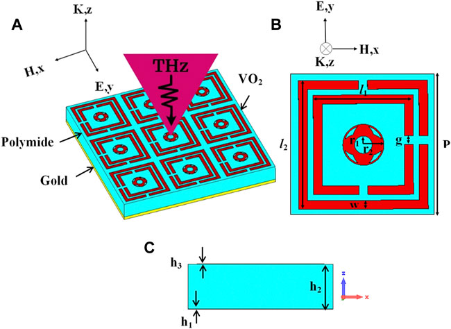
FIGURE 1. (A) A 3 × 3 perspective array of the proposed structure, (B) top view of the suggested unit cell, and (C) side view of the proposed unit cell.
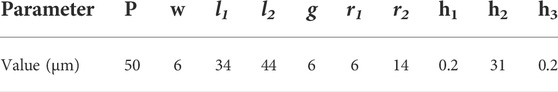
TABLE 1. The required dimensions of the suggested design.
Figure 2 shows the approach of presenting a step-by-step design of the proposed absorber. The design is a three-layer quatrefoil and circle-loaded complementary square split ring resonator shape that consists of three types of material (Gold-Polymide-VO2). This design is especially developed for easy production. The parametric dimensions of the proposed deign were purposely tuned by using parametric study and genetic algorithm to simulate the broad bands of perfect absorption in Terahertz frequency range. In the design 1 and 2, a double split-ring resonator was used and rotated with equivalent scales to observe how the traditional split ring resonator works in the terahertz regime. A fractal circular resonator was added to the center of the split rings, as shown in design 3 and 4, followed by examining its effect on the performance of the unit cell. Finally, the proposed design was selected by combining all the layouts in one single design (see Figure 2).
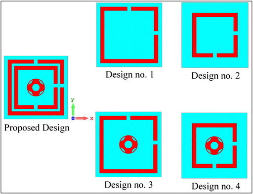
FIGURE 2. Front view of different design layouts used for selecting the final design.
The reflection responses and absorption capabilities of the studied layouts were comprehensively investigated, while absorptivity of the layouts was calculated using:
Where
Supported by Eq. (2) and Figure 3 shows that the absorptivity of all the layouts is inversely proportional to the reflection response. The absorption bandwidth of the layouts was compared at the corresponding absorption of 90%. The greater absorption bandwidth was observed for the design one in comparison to that of the design 2, which is the scaled and rotated version of the design 1. Moreover, the absorption bandwidth of the design 3 and 4, which was obtained by adding the fractal circular resonator, was almost at the same level of that for the design 1 and 2, respectively, as illustrated in Figure 3B. Finally, based on the achieved results, the proposed design was selected and the absorption bandwidth was studied in the frequency range from 0.58 to 1.65 THz, which corresponds to the absorption of 90% at 1.07 THz.
FIGURE 3. The simulated results of (A) reflection (S11) and (B) absorption as a function of frequency for different layouts.
One of the most important parameters is the split gap in a resonator design, which corresponds to a capacitive element in the resonator structure. The split ring resonator corresponds to an LC resonance circuit with resonance frequency as follows:
Where
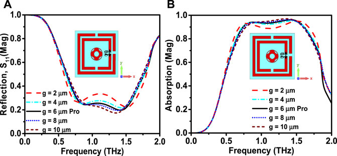
FIGURE 4. (A) Reflection coefficient and (B) Absorption coefficient change with the variation of the split gap.
Resonator line width is one of the other useful parameters which contribute in designing a split ring resonator. The split ring can be considered as a microstrip line, which has corresponding impedance given in Eq. 4 [37]:
Where the microstrip line width of
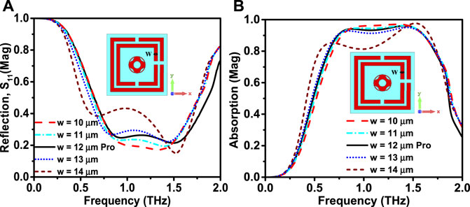
FIGURE 5. (A) Reflection coefficient and (B) absorption coefficient spectra with the change in the width of the resonator.
The substrate thickness (H) of the resonator, as shown in Eq. (4), presents a significant effect on the microstrip line impedance of the split ring resonator. In addition, the thickness variation changes the capacitive stabilization between the microstrip split ring line and back metallic ground. According to the mentioned criteria, the substrate thickness plays a significant role in the resonance characteristics. As shown in Figure 6, the change in the thickness from 28.8 to 32.8 µm has caused a clear change in the reflection and absorption characteristics. Consequently, the optimum thickness for the substrate was assigned to be 30.8 µm, leading to an improved bandwidth and absorption magnitude compared to those of the other thicknesses. It was seen that the simulation results at the substrate thickness of 29.8 and 30.8 µm are almost similar. Since the maximum bandwidth was achieved at 30.8 µm, we have chosen this dimension for the proposed design.
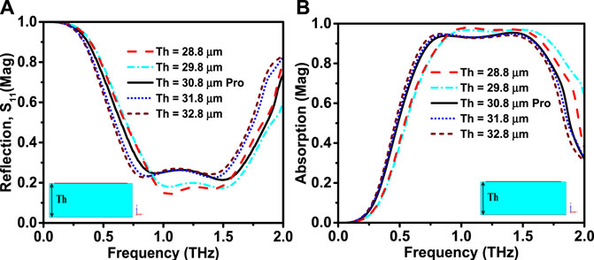
FIGURE 6. Simulated results of the effect of substrate thickness on the (A) reflection coefficient and (B) absorption coefficient of the resonators.
The effect of the radius of the central resonator on the absorption and reflection coefficient was also investigated. Technically, the change in the resonator radius corresponds to the change of the operating wavelength. This in turn causes the change in the resonance characteristics, as shown in Figures 7A,B for both reflection and absorption characteristics. According to the obtained results, the optimum radius of the inner resonator of the split ring is 14 µm for wideband applications at around one THz center frequency. Due to the parametric optimization results, the authors suggested to use 14 µm for the R dimension.
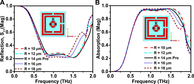
FIGURE 7. Simulated results of the effect of the resonator radius on the (A) reflection coefficient and (B) absorption coefficient.
The incident angle and polarization dependency of the proposed hybrid metamaterial were examined, as shown in Figure 8. When the step size of change in the incident angle was 15°, no significant change was observed in the absorption characteristics, as shown in Figure 8A. Due to symmetric and unique design of the proposed structure, a polarization and limited incident angle independency was achieved. The stable absorption characteristics confirmed the incident angle independence for the proposed structure under both TE and TM wave modes. Furthermore, another important phenomenon was investigated, which is the polarization dependency of the proposed design. According to the absorption characteristics given in Figure 8B, the proposed hybrid metamaterial has polarization independence under both TE and TM wave incidence around one THz. Both studied factors are specifically important in various application fields such as medical, military, stealth technology, and communication.
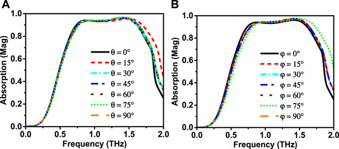
FIGURE 8. (A) The absorption spectrum for the suggested design at different incident angles and (B) the polarization-independent of the MTM unit cell from 0° to 90° for TM (or TE) modes.
In this section, taking into account different material properties of the proposed structure, the absorption mechanism of the proposed MTM absorber was investigated. First, the effect of the electrical conductivity and loss tangent of the metallic layer on the absorption response of the structure was simulated, as shown in Figure 9. This section was completely prepared by creating new material techniques in the CST. As such, the effect of loss tangent and conductivity on the absorption relation was ruled out. Figure 9A shows that the absorption response is more than 90% with a broad bandwidth of one THz over the frequency range of 0.7–1.7 THz, which is called a conducting (metallic) state with the conductivity of 3 × 10⁵ S/m. However, in the insulating state, when the conductivity is reduced to 3 × 10² S/m, the absorption is less than 5% in the frequency range of interest. As a result, the proposed absorber can be considered as a reconfigurable device with a dynamic absorption range of 3–90% in the frequency range of 0.7–1.7 THz. Moreover, Figure 9B shows the variation of the loss tangent, tanδ = 0.027, 0.0027, and 0.00027, for the proposed design. One can see that loss tangent has a trivial effect on the absorption response.

FIGURE 9. (A) Simulated results showing the absorption response at different conductivities of VO2, (B) at varied loss tangent of the proposed design, and (C) Absorption spectrum of the Gold-PI-VO2 structure and VO2-PI-Gold structure when VO2 is in the insulating state and (D) in the conducting (metallic) state.
In addition to the material properties, two different configurations were utilized aiming at investigating the absorption response of the structure. In the first configuration, the VO2 resonators were placed above PI substrate, which is backed by a gold ground plate (VO2-PI-Gold). However, in the second configuration, the resonators were made from gold, and the ground plate was formed from VO2 (Gold -PI- VO2). The two configurations were investigated in both insulating and conducting (metallic) states of the VO2 layer and the obtained results are illustrated in Figures 9C,D, respectively. Figure 9C shows the absorption spectrum of both configurations when VO2 is in the isolating state. The absorption spectrum in the first configuration, i.e.VO2-PI-Gold, was found to be more than 45% in comparison to the second configuration (Gold -PI- VO2), which was less than 20% in the frequency range of interest.
Noteworthy, a promising result was achieved when the VO2 was in the conducting state for the first configuration (Gold -PI- VO2), as shown in Figure 9D. Herein, the absorption spectrum was calculated to be more than 90% in the frequency range of 0.7–1.7 THz. In the second configuration of VO2-PI-Gold, only four absorption peaks were observed to be more than 90% at the frequencies of 0.67, 0.88, 1.5, and 1.8 THz. These results can be attributed to the VO2 resonators, which have an active role in producing multiple electric and magnetic resonances close to each other, leading to a broad absorption spectrum. The VO2 resonators are sensitive to the change in the constituent materials. Therefore, the resonators were no further responsible for producing the same resonances after changing VO2 properties and materials.
Figure 10 shows the performance of the proposed structure at different temperatures from 300 to 380 K. The temperature-dependent absorption response was investigated by importing the data of the change in the conductivity of VO2 into the numerical simulation. This was validated by considering the experimental effect of temperature on the conductivity of VO2 [38]. Results showed that the VO2 based resonator behaves in its insulating phase up to the temperature of 330 K, while beyond 330 K the VO2 becomes metallic due to the phase transition. It is worth mentioning that the absorption peak in the metallic state is at a lower frequency (red shifted) compared to that of the insulating state. This can be attributed to the plasmon resonance effect due to the interaction of incident photons with the free electrons of the metallic state. It is concluded that by the control of VO2 temperature, it is possible to manipulate the absorption band of the proposed MTM structure for desired applications.
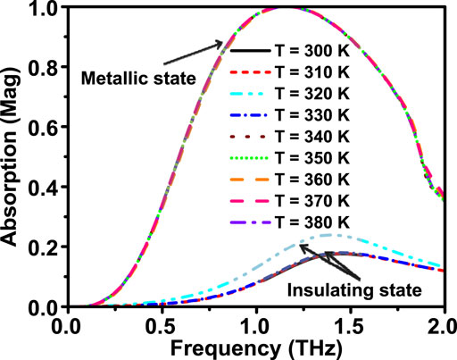
FIGURE 10. Absorption spectrum of the proposed metamaterial structure at different temperatures of VO2 in the insulating state and metallic state.
The use of flexible polyamide was motivated by its importance for the non-planar and conformal geometry applications, extending extra capabilities of the metamaterial for stealth technologies application. We carried out a simulation to show the effect of the structure curvature in the insulating state and conducting state, as shown in Figures 11A,B (b). It was found that when the proposed structure is bent, the absorption response between the operation channels is almost similar to that of the normal condition, as shown in Figure 9C. This is because of the resonator and VO2 properties. However, by looking at the VO2-Pl-Gold configuration, one can see a considerably lower absorption value. It was observed from Figure 11B that for the conducting sate when the structure is conformal, the absorption characteristics of the VO2 (Gold-PI-VO2) presented similar absorption peaks to that of the normal state (VO2-PI-Gold). In the metallic state, when the resonator is made of VO2 the absorption response is above 93% at higher frequency.
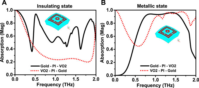
FIGURE 11. (A) Simulated results of absorption spectrum of Gold-PI-VO2 and VO2-PI-Gold structures when VO2 is in the insulating state and (B) in the metallic state (the whole structure is conformal).
To further verify the formation mechanism of the absorption and phase in degree response, we have numerically investigated the phase in degree corresponding frequency of interest for both insulating and metallic state as shown in Figure 12. It was seen from Figure 12A that a change in sign has occurred for the transmission phase at the first and second resonance dip. Also, peaks and dips at the insulating states were observed at the second resonance point during the transmission and reflection phases. In the metallic state, the transmission phase was suddenly changed at the resonance points, as can be seen in Figure 12B.
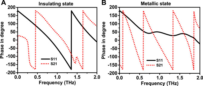
FIGURE 12. Simulated results of the phase degree for VO2 in the (A) insulating state and (B) metallic state.
The effect of waveguide ports on the performance of the proposed MTM device was investigated by deploying waveguide ports on the different axes of the structure. First, a pair of waveguide port was used at either side of the proposed structure along the X-axis with the existence of the primary ports along the Z-axis, as shown in Figure 13A. As can be seen from Figure 13B, the S21 curve is below −10 dB from the starting frequency to about 1.2 THz with two resonance frequencies at 0.8, and 1.2 THz having the reflection values of −25 dB and −21dB, respectively. However, the S11 curve is below −10 dB from the starting frequency to 2 THz, except at the center frequencies of the band, for which it was above 10 dB from 0.7 to 1.2 THz, with a relatively similar fluctuation in the S21 response.
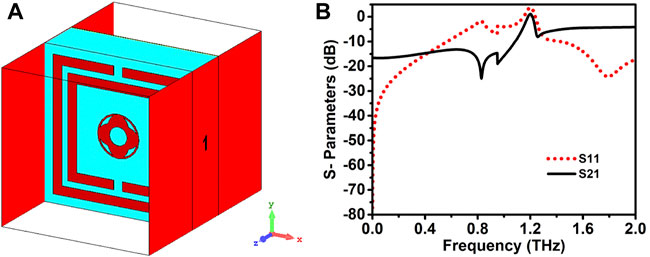
FIGURE 13. (A) The simulated setup showing wave propagation in the x-axis and (B) S-parameters.
In the second case, the waveguide ports were utilized along the Y-axis in the same manner, as in the first case shown in Figure 14A. The results of Figure 14B showed that S21 value is below 10 dB from the starting frequency to 1.2 THz, with observing two resonances at 0.8 THz, and 1.2 THz having values of −25 dB and—21 dB, respectively. Noticeably, the S11 curve is below −10 dB from the starting frequency up to 2 THz, while in the range from 0.7 to 1.2 THz, the S-parameters are above 10 dB. Similar results were observed in deploying the waveguide ports along the x or y-axis, as shown in Figure 13B, implying the independence of the axes on the wave propagation.
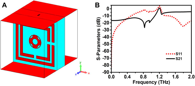
FIGURE 14. (A) Simulated set up structure for the wave propagation in the y-axis direction and (B) spectrum of the S-parameters.
In this section, the proposed broadband metamaterial absorber was analyzed by utilizing different unit cell arrangements. Generally, a number of absorber unit cells and arrangements are required for different applications. For example, the 1 × 2 array is mostly utilized as a decoupling structure between antenna elements of a large antenna array. However, in military radar applications, large numbers of unit cell arrangements are used to cover a large area. Therefore, it is crucial to investigate different absorber arrangements before being applied in any desired applications.
This section aims to give a useful idea to the reader on how to present the periodic and unit cell boundary conditions. Unit cell and periodic boundary conditions are similar to each other. With Unit Cell boundary conditions and floquet port, we can get the amplitude and phase of the transmitted and reflected waves. So Unit Cell boundary conditions are mostly used for designing elements of reflects array and metasurfaces. With periodic boundary condition, we can consider phase shift along the axes and it is mostly used for getting dispersion diagram of a unit cell. For this reason, different array structures were presented and simulated.
Figure 15 shows the configuration of a 1 × 2 array structure along with the obtained results. For the precise calculation, similar environment and conditions of the proposed structure were set for the 1 × 2 array structure. The reflection and absorption coefficient spectra were compared with the result of the proposed unit cell structure, as shown in Figures 15B,C. It can be observed from the figures that the proposed structure presents a relatively similar result. This is where the reflection of less than 0.3 was realized, corresponding to the absorption of more than 90% over the frequency range of 0.7–1.7 GHz. It is worth to mention that the absorption of the 1 × 2 array structure was lower than that of the proposed design by about 2%.

FIGURE 15. (A) 1 × 2 array simulated structure, (B) its reflection and (C) absorption spectra.
Using similar procedure to that of the 2 × 1 array structure, the 2 × 2 and 3 × 3 array structures were also designed with their boundary conditions, as shown in Figures 16A, 17A. The obtained reflection and absorption coefficient from both arrangements (2 × 2 and 3 × 3 array) were also compared with the results of the proposed absorber, which is presented in Figures 16B,C, 17(b), and Figure 17C, respectively. The obtained results indicated that the absorption spectrum of both arrangements is almost similar to that of the proposed structure, in which a broad bandwidth of THz with the absorption of more than 90% was achieved over the frequency range of 0.7–1.7 GHz. This result showed that the stability of the absorber is acceptable for the practical applications.
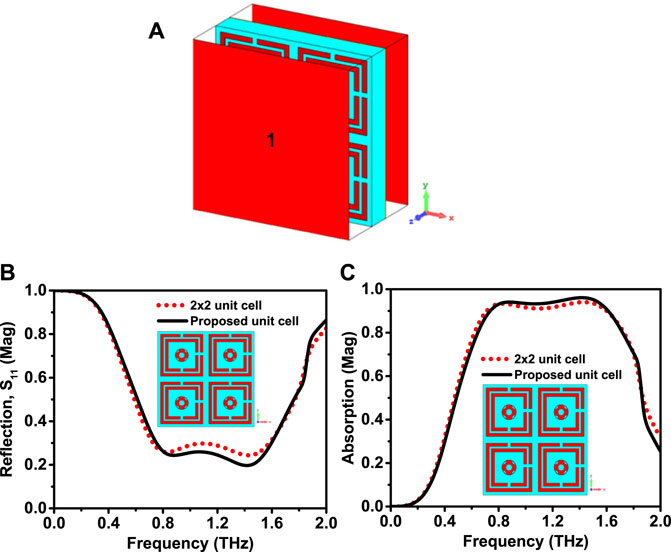
FIGURE 16. (A) Simulated 2 × 2 array structure, (B) its reflection and (C) absorption spectra.
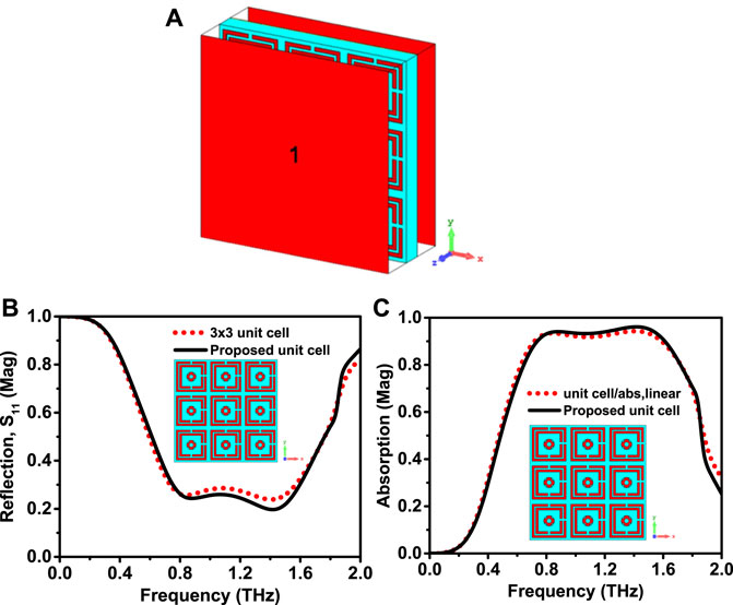
FIGURE 17. (A) 3 × 3 array simulated design, (B) its reflection and (C) absorption spectra.
Further investigations were finally made on a 4 × 4 array structure, as shown in Figure 18A. The simulated results of the reflection and absorption responses for the 4 × 4 array absorber were also monitored and presented in Figure 18. It was noted from Figure 18B,C that the reflection and absorption results of the 4 × 4 array structure are similar to that of the proposed results, except for the presence of a small absorption reduction in the lower frequency range from 0.7 to one THz, which is below 90%.
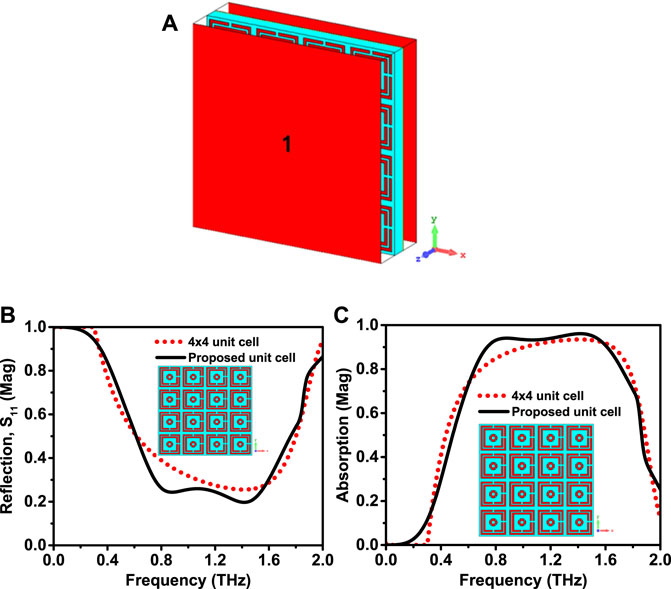
FIGURE 18. (A) Simulated setup for the 4 × 4 array design, (B) its reflection, and (C) absorption spectra.
Theoretically, for a perfect absorber to be achieved the reflection and transmission spectra should be zero [39]. In this situation, the absorbance can reach maximum at a resonance frequency of interest, as can be seen from Eq. (2). The reflectance becomes zero if the impedance of the structure (Z) is equal to the impedance of the free space. To maximize the absorbance at the resonant frequency, transmission (T) needs to be at minimum. For an ideal absorber, the real part of Z should be one and the imaginary part should approach zero at a resonance frequency.
It is seen from Figure 19A that the operating band is between 0.7 and 1.7 THz. Moreover, the real part of the impedance is one throughout the operating band and the imaginary part is 0, which makes the proposed structure a good absorber. In the equivalent circuit diagram, the resistive and inductive components (R and L) are mainly attributed to the VO2 structure in the resonator layer, as shown in Figure 19D. Figure 19C shows the equivalent circuit of the designed unit cell, where R1 and L1 denote the resistance and inductance of the inner circular shape, while R2 and R3 define the resistance of the inner and outer rectangular strips, respectively. The equivalent capacitance Ceq1 and Ceq(2) represent the total capacitance of the inner and outer rectangular strips, respectively. Hence, a double mutual inductance can be presented between the L1, L2, and L3, where L2 and L3 are the inductance of the inner and outer rectangular strips, respectively. The relative impedance contains both real and imaginary parts as a function of frequency is shown in Figure 19D. During this study, due to the parametric optimization and author experiences, the CST software was chosen.
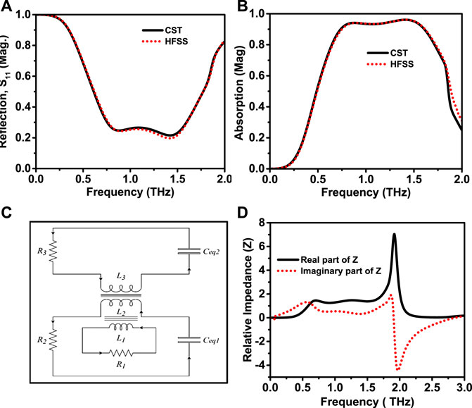
FIGURE 19. (A) Comparison of the simulated CST and HFSS software for the reflection spectra (B), absorption coefficient, (C) equivalent circuit diagram and (D) real and imaginary part of the impedance for the proposed structure.
The surface current distribution, E-field, and H-fields of the proposed absorber are illustrated in Figures 20–22, respectively. The relation between these three can be understood by Maxwell’s equation which relates the magnetic field with the electric field and current distribution as below:
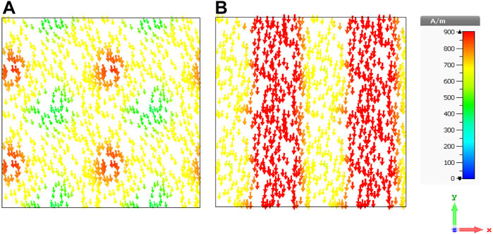
FIGURE 20. Surface current distribution at two different resonance peaks of (A) 0.88 THz and (B) 1.42 THz.
Also, the relation between the electric field and current density is:
It can be observed from Figure 17 that the currents are flowing dominantly along the y-axis. It is also seen that the flow of current is weak at 0.88 THz compared to that at 1.42 THz.
As a stable and disperse E-field, the proposed structure showed a well-disseminated H-field for two frequencies. However, Figure 21 shows that E-field is very intensive with a little degradation at the split-ring resonators. The H-field is located on the fractal circular resonator at 0.88 THz compared to 1.42 THz and it is widely confined by the dielectric substance of the structure, as can be seen in Figure 22. The current density that is closely connected with the H-field increases the artificial magnetic dipolar moment [40]. The electromagnetic field distribution in Figures 21, 22 is along z-axis and does not represent its absolute value. The arrangement then excites the H-field and hints at a very powerful magnetic resonant dipole and produces an excellent absorption in the entire optical region.
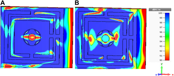
FIGURE 21. Simulated electric field distribution for the MTM unit cell at (A) 0.88 THz and (B) 1.42 THz.
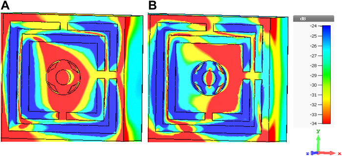
FIGURE 22. Magnetic field distribution for the suggested structure at (A) 0.88 THz and (B) 1.42 THz.
In summary, a flexible broadband metamaterial based on VO2 structure was theoretically developed for the terahertz applications. The suggested design is made of VO2/Polyimide/Gold from top to bottom. According to the results of using two different software, CST and HFSS, for our designed structure, the proposed structure showed a good agreement and consistency over a large absorption of more than 90%. It was noticed that when the VO2 is in the metallic state, the bandwidth of the absorption spectrum reached 1.34 THz, while the absorption was greater than 90%. Different design layouts, different waveguide port axes, and unit cell structures (1 × 2, 2 × 2, 3 × 3, and 4 × 4 arrays) were investigated and compared numerically in order to obtain the final proposed design. The flexible nature of the proposed MTM design makes it a viable candidate for the non-planar and conformal geometry applications, in stealth technology, and terahertz imaging.
The original contributions presented in the study are included in the article/Supplementary Material, further inquiries can be directed to the corresponding author.
All co-authors are contributed this work as bellow: YA and MK conceived the idea; YA and HA performed the simulations; YA, HA, FA, MB, OA, FM wrote the manuscript; SS, MK, MT, BA, JD and revised the manuscript; JD and YA supervises this work.
This research was funded in part by the National Natural Science Foundation of China, Grant Number 61801521 and 61971450, in part by the Natural Science Foundation of Human Province, Grant Number 2018JJ2533 and 2022JJ30052, and in part by the Fundamental Research Funds for the Central Universities, Grant Number 2018gczd014 and 20190038020050.
The authors declare that the research was conducted in the absence of any commercial or financial relationships that could be construed as a potential conflict of interest.
All claims expressed in this article are solely those of the authors and do not necessarily represent those of their affiliated organizations, or those of the publisher, the editors and the reviewers. Any product that may be evaluated in this article, or claim that may be made by its manufacturer, is not guaranteed or endorsed by the publisher.
1. Sikam P, Thirayatorn R, Moontragoon P, Kaewmaraya T, Amornkitbamrung V, Ikonic Z, et al. The quantum-confined Stark effect in N-doped ZnO/ZnO/N-doped ZnO nanostructures for infrared and terahertz applications. Nanotechnology (2020) 31(44):445207. doi:10.1088/1361-6528/aba86f
2. Yang Y, Yamagami Y, Yu X, Pitchappa P, Webber J, Zhang B, et al. Terahertz topological photonics for on-chip communication. Nat Photon (2020) 14(7):446–51. doi:10.1038/s41566-020-0618-9
3. D’Arco A, Di Fabrizio M, Dolci V, Petrarca M, Lupi S THz pulsed imaging in biomedical applications. Condensed Matter (2020) 5(2):25. doi:10.3390/condmat5020025
4. Xie Y, Liang F, Chi S, Wang D, Zhong K, Yu H, et al. Defect engineering of MoS2 for room-temperature terahertz photodetection. ACS Appl Mater Inter (2020) 12(6):7351–7. doi:10.1021/acsami.9b21671
5. Li J, Papasimakis N, MacDonald KF, Zheludev NI Optical magnetic response without metamaterials. APL Photon (2021) 6(7):071303. doi:10.1063/5.0054752
6. Ren Z, Xu J, Le X, Lee C Heterogeneous wafer bonding technology and thin-film transfer technology-enabling platform for the next generation applications beyond 5G. Micromachines (2021) 12(8):946. doi:10.3390/mi12080946
7. Xu H, Bi K, Hao Y, Zhang J, Xu J, Dai J, et al. Switchable complementary diamond-ring-shaped metasurface for radome application. IEEE Antennas Wirel Propag Lett (2018) 17(12):2494–7. doi:10.1109/lawp.2018.2879474
8. Duan G, Schalch J, Zhao X, Li A, Chen C, Averitt RD, et al. A survey of theoretical models for terahertz electromagnetic metamaterial absorbers. Sensors Actuators A: Phys (2019) 287:21–8. doi:10.1016/j.sna.2018.12.039
9. Shen Y, Zhang J, Wang J, Pang Y, Ma H, Qu S, et al. Multistage dispersion engineering in a three-dimensional plasmonic structure for outstanding broadband absorption. Opt Mater Express (2019) 9(3):1539. doi:10.1364/ome.9.001539
10. Tao H, Landy NI, Bingham CM, Zhang X, Averitt RD, Padilla WJ, et al. A metamaterial absorber for the terahertz regime: Design, fabrication and characterization. Opt Express (2008) 16(10):7181. doi:10.1364/oe.16.007181
11. Chen F, Cheng Y, Luo H Temperature tunable narrow-band terahertz metasurface absorber based on InSb micro-cylinder arrays for enhanced sensing application. IEEE Access (2020) 8:82981–8. doi:10.1109/access.2020.2991331
12. Wanga Y, Yib Y, Xu D, Yi Z, Li Z, Chen X, et al. Terahertz tunable three band narrowband perfect absorber based on Dirac semimetal. Physica E: Low-dimensional Syst Nanostructures (2021) 131:114750. doi:10.1016/j.physe.2021.114750
13. Jun W Tunable multi-band terahertz absorber based on graphene nano-ribbon metamaterial. Phys Lett A (2019) 383(22):2589–93. doi:10.1016/j.physleta.2019.05.020
14. Tong X, Chen D, Xua Y, Wang Y, Li M, Zhang Z, et al. High absorption and a tunable broadband absorption based on the fractal Technology of Infrared Metamaterial Broadband Absorber. Diamond Relat Mater (2022) 123:108872. doi:10.1016/j.diamond.2022.108872
15. Chen F, Cheng Y, Luo H A broadband tunable terahertz metamaterial absorber based on single-layer complementary gammadion-shaped graphene. Materials (2020) 13(4):860. doi:10.3390/ma13040860
16. Cheng Y, Zhao H, Chan L Broadband tunable terahertz metasurface absorber based on complementary-wheel-shaped graphene. Opt Mater (2020) 109(1):110369. doi:10.1016/j.optmat.2020.110369
17. Song Z, Wang K, Li J, Liu QH Broadband tunable terahertz absorber based on vanadium dioxide metamaterials. Opt Express (2018) 26(6):7148. doi:10.1364/oe.26.007148
18. Zhang Y, Qiao S, Sun L, Shi QW, Huang W, Li L, et al. Photoinduced active terahertz metamaterials with nanostructured vanadium dioxide film deposited by sol-gel method. Opt Express (2014) 22(9):11070. doi:10.1364/oe.22.011070
19. Liang J, Hou L, Li J Frequency tunable perfect absorber in visible and near-infrared regimes based on VO_2 phase transition using planar layered thin films. J Opt Soc Am B (2016) 33(6):1075. doi:10.1364/josab.33.001075
20. Lv TT, Li YX, Ma HF, Zhu Z, Li ZP, Guan CY, et al. Hybrid metamaterial switching for manipulating chirality based on VO 2 phase transition. Sci Rep (2016) 6(1):23186. doi:10.1038/srep23186
21. Wang S, Kang L, Werner DH Active terahertz chiral metamaterials based on phase transition of vanadium dioxide (VO 2). Sci Rep (2018) 8(1):189. doi:10.1038/s41598-017-18472-x
22. Sun K, Riedel CA, Urbani A, Simeoni M, Mengali S, Zalkovskij M, et al. VO2 thermochromic metamaterial-based smart optical solar reflector. ACS Photon (2018) 5(6):2280–6. doi:10.1021/acsphotonics.8b00119
23. Chu Q, Song Z, Liu QH Omnidirectional tunable terahertz analog of electromagnetically induced transparency realized by isotropic vanadium dioxide metasurfaces. Appl Phys Express (2018) 11(8):082203. doi:10.7567/apex.11.082203
24. Song Z, Deng Y, Zhou Y, Liu Z Terahertz toroidal metamaterial with tunable properties. Opt Express (2019) 27(4):5792. doi:10.1364/oe.27.005792
25. Wang T, Zhang Y, Zhang H, Cao M Dual-controlled switchable broadband terahertz absorber based on a graphene-vanadium dioxide metamaterial. Opt Mater Express (2020) 10(2):369. doi:10.1364/ome.383008
26. Liu H, Wang ZH, Li L, Fan YX, Tao ZY Vanadium dioxide-assisted broadband tunable terahertz metamaterial absorber. Sci Rep (2019) 9(1):5751. doi:10.1038/s41598-019-42293-9
27. Huang J, Li J, Yang Y, Li J, Li J, Zhang Y, et al. Broadband terahertz absorber with a flexible, reconfigurable performance based on hybrid-patterned vanadium dioxide metasurfaces. Opt Express (2020) 28(12):17832. doi:10.1364/oe.394359
28. Zhu H, Zhang Y, Ye L, Li Y, Xu Y, Xu R, et al. Switchable and tunable terahertz metamaterial absorber with broadband and multi-band absorption. Opt Express (2020) 28(26):38626. doi:10.1364/oe.414039
29. Ren W, Huang W, Zhu H, Wang bD, Zhu L-G, Shi Q, et al. Flexible VO2/Mica thin films with excellent phase transition properties fabricated by RF magnetron sputtering. Vacuum (2021) 192:110407. doi:10.1016/j.vacuum.2021.110407
30. Li C-I, Lin J-C, Liu H-J, Chu M-W, Chen H-W, Ma C-H, et al. van der Waal epitaxy of flexible and transparent VO2 film on muscovite” chem. Mater (2016) 28(11):3914–9.
31. Liu Y-X, Cai Y, Zhang Y-S, Deng X, Ni Z, Xiang P-H, et al. Van der Waals epitaxy for high-quality flexible VO2 film on mica substrate. J Appl Phys (2021) 130:025301. doi:10.1063/5.0046827
32. Kim J, Paik T Recent advances in fabrication of flexible, thermochromic vanadium dioxide films for smart windows. Nanomaterials (Basel) (2021) 11(10):2674. doi:10.3390/nano11102674
33. Zhang C, Zhou G, Wu J, Tang Y, Wen Q, Li S, et al. Active control of terahertz waves using vanadium-dioxide-embedded metamaterials. Phys Rev Appl (2019) 11(5):054016. doi:10.1103/physrevapplied.11.054016
35. Sengupta K, Nagatsuma T, Mittleman DM Terahertz integrated electronic and hybrid electronic–photonic systems. Nat Electron (2018) 1(12):622–35. doi:10.1038/s41928-018-0173-2
36. Elayan H, Amin O, Shubair RM, Alouini MS Terahertz communication: The opportunities of wireless technology beyond 5G. In: 2018 International Conference on Advanced Communication Technologies and Networking (CommNet), 2–4 April 2018, Marrakech, Morocco (2018). p. 1–5. IEEE.
37. Yang LL, Sun L, Shi Q, Sun HY Extraction of dielectric constant based on S-parameter inversion method. In: 2011 3rd International Conference on Computer Research and Development; 11th to 13th March 2011; Shanghai, China, 3 (2011). p. 353–6.
38. Chang YJ, Yang JS, Kim YS, Kim DH, Noh TW, Kim DW. Surface versus bulk characterizations of electronic inhomogeneity in aVO2thin film. Phys Rev B (2007) 76:075118. doi:10.1103/physrevb.76.075118
39. Salman D, Prince B Right-angle shaped elements as dual-band metamaterial absorber in terahertz. Photonic Sens (2020) 10:233–41. doi:10.1007/s13320-019-0573-6
Keywords: metamaterial absorber, dual-band, polarization-independent, complementary square split ring resonator, vanadium dioxide
Citation: Abdulkarim YI, Awl HN, Muhammadsharif FF, Bakır M, Alkurt FÖ, Altıntaş O, Saeed SR, Taouzari M, Karaaslan M, Appasani B and Dong J (2022) A vanadium dioxide-based metamaterial with quatrefoil and circle loaded structure on flexible polyamide substrate for terahertz applications. Front. Phys. 10:968310. doi: 10.3389/fphy.2022.968310
Received: 13 June 2022; Accepted: 12 July 2022;
Published: 17 August 2022.
Edited by:
Huabin Wang, Chongqing Institute of Green and Intelligent Technology (CAS), ChinaReviewed by:
Fei Fan, Nankai University, ChinaCopyright © 2022 Abdulkarim, Awl, Muhammadsharif, Bakır, Alkurt, Altıntaş, Saeed, Taouzari, Karaaslan, Appasani and Dong. This is an open-access article distributed under the terms of the Creative Commons Attribution License (CC BY). The use, distribution or reproduction in other forums is permitted, provided the original author(s) and the copyright owner(s) are credited and that the original publication in this journal is cited, in accordance with accepted academic practice. No use, distribution or reproduction is permitted which does not comply with these terms.
*Correspondence: Jian Dong, ZG9uZ2ppYW5AY3N1LmVkdS5jbg==
Disclaimer: All claims expressed in this article are solely those of the authors and do not necessarily represent those of their affiliated organizations, or those of the publisher, the editors and the reviewers. Any product that may be evaluated in this article or claim that may be made by its manufacturer is not guaranteed or endorsed by the publisher.
Research integrity at Frontiers
Learn more about the work of our research integrity team to safeguard the quality of each article we publish.