 Abderrezak Boughedda
 Saida Latreche2
 Maya Lakhdara
 Gian-Franco Dalla Betta
94% of researchers rate our articles as excellent or good
Learn more about the work of our research integrity team to safeguard the quality of each article we publish.
Find out more
BRIEF RESEARCH REPORT article
Front. Phys., 07 July 2022
Sec. Radiation Detectors and Imaging
Volume 10 - 2022 | https://doi.org/10.3389/fphy.2022.957089
A design modification to an existing 3D-trenched pixel detector is proposed, aimed at an improved fabrication yield. The device concept is studied and its performance is evaluated by TCAD simulations, in comparison to the existing one. Although the modified design features a less uniform electric field distribution, it is still expected to yield a very good timing performance and high radiation tolerance, also exploiting charge multiplication effects.
The High Luminosity upgrade of the LHC (HL-LHC) [1] and future post-LHC colliders (e.g., the Future Circular Collider (FCC) [2]) will feature extremely high particle collision rates, leading to unprecedented radiation levels and event pile-up in the detectors. At HL-LHC, the innermost layers of tracking systems will experience radiation fluences
The peculiar geometry of 3D detectors make them intrinsically fast devices [6], but the first study about their timing properties was only published in 2011 [7], reporting timing resolution from ∼30 ps to ∼180 ps in non-optimized test structures. Recently, a small-pitch (50 μm × 50 μm) 3D single-pixel test structure fabricated at CNM (Barcelona, Spain) was tested using a fast discrete readout channel, showing a timing resolution of ∼30 ps at 150 V bias and −20°C [8] and still lower than 50 ps after irradiation up to 1 × 10¹⁶ neq/cm2 [9]. These remarkable results are however limited by the spatial non-uniformity of the electric and weighting fields within a pixel, which are typical of 3D sensors [6, 7].
As proposed in [7], replacing columnar electrodes with trenched electrodes can further improve the timing resolution of 3D detectors. Trenched electrodes were introduced in 2001 at the Stanford Nanofabrication Facility as a precursor to active edges [10], but they have not been fully developed, and until recently only a few studies have been reported about devices not intended for timing applications [11, 12]. Since 2018, a dedicated R&D effort has been pursued within the INFN TIMESPOT project, in collaboration with FBK (Trento, Italy) [4, 13–15]. Small-pitch 3D-trenched detectors were designed with the aid of TCAD simulations [13], fabricated and tested, showing very good electrical characteristics [14]. Test structures coupled to fast SiGe discrete front-end circuits were tested at PSI with a beam of 270 MeV/c pions, showing an outstanding timing performance (
These very promising results come at the expense of a complex technology, which has still to be optimized in terms of yield. In this respect, possible simplifications of the pixel layout will be beneficial. Therefore, we have studied a modified 3D-trench pixel sensor concept, that is presented in this paper along with results from TCAD simulations.
The single-sided process developed for the ATLAS ITk 3D sensors [17] has been adapted at FBK for the fabrication of 3D-trenched pixels [14]. A device cross-section is shown in Figure 1A. The active layer is a high-resistivity, p-type Float Zone Silicon wafer with a thickness of 150 μm directly bonded to a 500 μm thick, low-resistivity p-type handle substrate. The p+ (ohmic) trenches are etched by Deep Reactive Ion Etching (DRIE) deeper than the active layer, so as to reach the p++ handle wafer where a good ohmic contact is obtained for back-side sensor bias. In order to ease wire bonding, the handle wafer can be thinned with a post processing and a metal layer can be deposited. The etching of the n+ (junction) trenches instead stops at a short distance (∼20 μm) from the p++ handle wafer, so as to avoid early breakdown. Both trench types are at least partially filled with poly-Silicon, which also extends laterally at the trench opening (so called poly-caps). Contacts are opened in the oxide layer covering the n+ poly-cap to connect the n+ trenches to the metal layer, where bump pads are opened in the passivation layer. A p-spray layer (not shown) prevents the inversion of the surface at the front side and ensure isolation of the n+ trenches. Figure 1B shows the layout of two adjacent pixels of 55 μm × 55 μm size, compatible with the readout chips of the TIMEPIX family. The n+ trench width is 40 μm, which is a good trade-off between the intrinsic response time and the capacitance [13]. In order to accurately reproduce the layout details, stepper lithography is used [18].
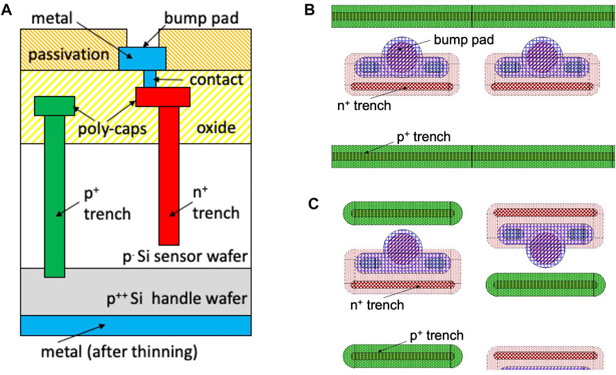
FIGURE 1. 3D-trenched-electrode pixel: (A) schematic cross-section (not to scale); layouts of two adjacent pixels of 55 × 55 μm2 size in (B) existing device and (C) proposed device.
From the fabrication yield viewpoint, the most critical layout aspect in Figure 1B is the continuous p+ trench, which ensures the maximum uniformity in the distributions of the electric field and weighting field [4, 13]. In the existing prototypes [14] the p+ trench is a few mm long, and it could reach over 1 cm in full scale devices. Continuous p+ trenches were found to be the regions with the highest density of defects at FBK, as observed after the lithography of the related poly-caps. These defects are mainly attributed to the formation of bubbles in the photoresist due to a non perfect filling of the trenches with poly-silicon. In comparison, test structures from the same wafers featuring dashed p+ trenches exhibited a significantly lower defect density. This difference was previously observed at FBK between active edges and slim edges in planar detectors [19].
This observation motivated us to investigate a modified pixel design featuring dashed p+ trenches. In the proposed layout (Figure 1C), the placements of the n+ and p+ trenches, that are both 40 μm wide, are swapped. Considering the same pixel size of 55 × 55 μm2 of the existing device, this layout variant is still compatible with a regular (square) footprint of bump bonding pads in the readout chip, provided that the bump bonding pads in the pixels of even rows are vertically flipped, so that their center is vertically aligned to those of adjacent pixels in odd rows. Of course a half-pitch vertical offset between even and odd rows should be taken into account for particle hit point reconstruction, and the design of the edge termination at the sensor periphery should also be modified.
TCAD simulations were performed by Synopsys Sentaurus. Since in 3D sensors the electric field in the vertical direction is uniform along most of the sensor thickness, a simplified quasi-2D simulation domain was used, consisting of a 1 μm thick slice taken at half the depth of the active layer. Although this does not account for surface effects and for particle tilt effects, it was deemed appropriate for a first validation of the idea. The simulated structures consist of two adjacent quarters of a pixel (Figures 2A,B), exploiting the inherent 3D cell symmetry to minimize the number of grid points and the computational effort.
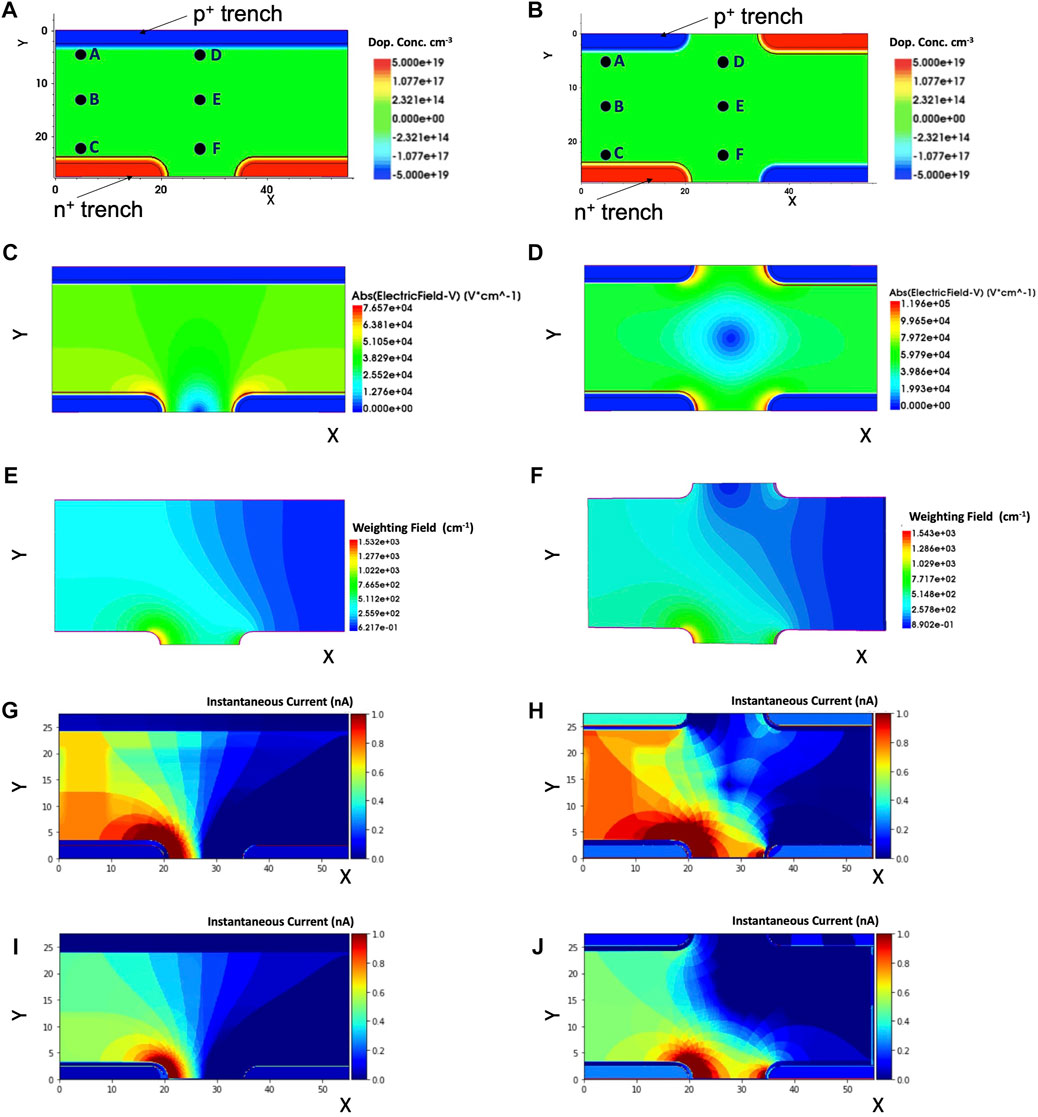
FIGURE 2. Simulation domains for (A) existing device and (B) proposed device, also showing the particle hit points (all dimensions in micrometers); distributions of the electric field at 100 V bias voltage for (C) existing device and (D) proposed device; distributions of the weighting field for (E) existing device and (F) proposed device. Ramo maps for electrons and holes at 100 V bias voltage: (G) existing device, electrons; (H) proposed device, electrons; (I) existing device, holes; (J) proposed device, holes.
Simulations use typical models (e.g., effective intrinsic density, doping dependent Shockley-Read-Hall generation/recombination and mobility, high field saturation, etc.) and default values for most parameters but the minority carrier lifetimes, for which values of 1 ms were chosen, typical of FBK technology. Impact ionization effects are incorporated according to the avalanche model by Van Ovestraeten/De Man. Bulk radiation damage effects are simulated using the CERN model [20], that is tuned for p-type silicon. This model was initially validated for a temperature range from −38.1°C to −31.1 (here we use −37.9°C) up to a radiation fluence of 8 × 10¹⁵ neq/cm2. However, we have previously demonstrated that simulation results in terms of signal efficiency (i.e., the ratio of the charge signal amplitude after irradiation and before irradiation) are accurate up to 2 × 10¹⁶ neq/cm2 [21], so the model is here used up to this higher limit.
The electrical characteristics are studied by a quasi-static analysis, which also saves the bias voltage conditions to be later fed as initial conditions for the transient analysis. In particular, applying Ramo’s theorem [22], two-dimensional maps of the instantaneous current, i, induced at the electrodes by the charge carriers moving along their drift paths, are calculated as i = qEw ⋅ vd, where q is the elementary charge, Ew is the weighting field and vd is the carrier drift velocity. To simulate the weighting field, a 1 V voltage was applied to the readout electrode (bottom-left n+ trench), with all the other electrodes grounded, and the silicon bulk was replaced with an insulating layer. In order to optimize the timing resolution, the Ramo maps should be as uniform as possible, which, in turn, requires both the weighting field distribution and the carrier velocity (hence the electric field) distribution to be as uniform as possible. Ideally, vd should be saturated, which in 3D sensors is feasible at a relatively low bias voltage, owing to the short inter-electrode distance.
Minimum Ionizing Particles (MIPs) are emulated by using the “HeavyIon” model: charge packets of 80 electron-hole pairs are released at different hit positions with a uniform distribution along the vertical axis and a Gaussian distribution across the horizontal plane of 0.25 μm width. The simulated hit points, that were chosen as representative of different electric field and weighting field conditions, are shown in Figures 2A,B. To study the signal dynamics and charge collection properties, transient simulations are performed, providing as an output current pulses at the readout electrodes as a function of time. The leakage current is subtracted from the current pulse and a numerical integration in the time domain is performed over 20 ns (compatible with LHC bunch-crossing), yielding the charge signal.
A summary of the results for non irradiated structures is reported in Figures 2C–J. The distributions of the electric field at 100 V bias voltage are shown in Figures 2C,D. The electric field is very uniform in the existing device, and high enough for saturation of carrier velocity in most of the active volume. On the contrary, a weak spot in the map is evident at the center of the simulation domain in the modified device, as a result of the inherent asymmetries in the placement of n+ and p+ trenches. This is clearly a disadvantage, but it should be noted that a similar problem also affects the existing device, though in different positions: in between the n+ trenches (Figure 2C), and inside the trenches, which are dead regions. Thus, the problem of the low-field region in the modified design is compensated by the increased geometrical efficiency obtained by the segmentation of the p+ trenches. It is also worth noting that the electric field peaks at the trench corners are higher in the modified design, due to the close proximity between adjacent n+ and p+ trenches. This could be a concern for early breakdown, but could also enhance charge multiplication effects at high voltage and boost the signal efficiency after irradiation.
The weighting field distributions simulated for the bottom-left n+ trench readout electrode are shown in Figures 2E,F. Results are comparable for the two structures. Ramo maps for electron and holes at 100 V bias voltage are shown in Figures 2G–J. For the existing device, results match those reported in [4], and confirm that most of the pixel volume can give large contribution to the induced current. The situation is slightly worse in the modified design, because of the previously described weak spot of electric field in the center of the simulation domain.
The pixel capacitance was also simulated, showing slightly lower (∼−20%) values in the modified design, mainly due to a smaller contribution from the opposite electrode. Of course the quasi-2D simulation does not include surface effects (e.g., MOS effects from the overlap of poly-cap and metal pad on silicon), but these are expected to be the same for both type of devices since the layout is exactly the same.
Figures 3A,B show the current signals as a function of time at a bias voltage of 100 V for the different MIP hit points of Figures 2A,B. The data correspond to the sum of the currents of two n+ trenches. As expected, results are very similar for hit points A, B, and C, where the electric field and weighting field are almost the same in the two designs, with very fast rise times and a maximum duration of 400 ps. More significant differences are observed for hit points D, E, and F, which belong to the boundary between the two adjacent pixels. In the existing device, signals are still very fast for points D and E, whereas for point F the shape is quite different with an attenuated primary peak, due to electrons, and a more pronounced secondary peak, due to holes. In the modified design, signals for points D and F (which have exactly the same shape due to the pixel symmetry, since the two n+ trench currents are summed) are comparatively faster than for point F of the existing device, owing to slightly larger electric field and weighting field. On the contrary, for point E, the signal is considerably delayed, with a much longer rise time and a total duration of ∼ 800 ps. In fact point E is exactly at the center of the weak spot of electric field, so charge carriers have to initially diffuse before finding a sufficiently high electric field [6].
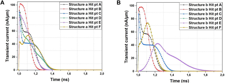
FIGURE 3. Simulated current signals as a function of time at 100 V bias voltage for different MIP hit points: (A) existing device, and (B) proposed device.
As previously mentioned, a delayed signal would cause a degradation of the timing performance, exactly as it would happen in the existing device if a particle would hit inside a trench. This problem can be strongly mitigated by tilting the sensor plane with respect to the particle direction by a few degrees, that is a typical solution adopted with 3D sensors [23]: the tilt of the particles leads to average out the effects of the non-ideal distributions of the electric and weighting field, yielding very fast rise times. In addition, full 4D-tracking systems should preferably use multiple planes of 3D-trenched sensors with an offset between the electrodes, so that most particle tracks would traverse sensor volumes away from low field regions [7].
The signal efficiency is shown in Figure 4 as a function of the applied voltage and for different fluences. Data refer to the sum of the charges collected at the two nˆ+ trenches. Figures 4A–F compare the results for different hit points at three different fluences (5 × 10¹⁵, 1 × 10¹⁶, and 2 × 10¹⁶ neq/cm2). For hit points A–C, results are very similar in the entire voltage range, as expected. On the contrary, for hit points D–F, more significant differences are observed: in particular, charge multiplication effects are evident in the modified design for points D and F starting at ∼ 150 V (the two data sets are overlapped in Figures 4B,D,F), that are not present in the existing device. In fact, in the modified design, the electric field at the trench edges, enhanced by the larger “effective doping concentration” in the bulk induced by the traps after irradiation, is high enough to start impact ionization. For hit point E, the weak spot of electric field, that is also present after irradiation and whose size increases with fluence, reduces the signal efficiency at low voltage, with gradually lower values with increasing fluence, until charge multiplication effects finally boost it at large voltage.
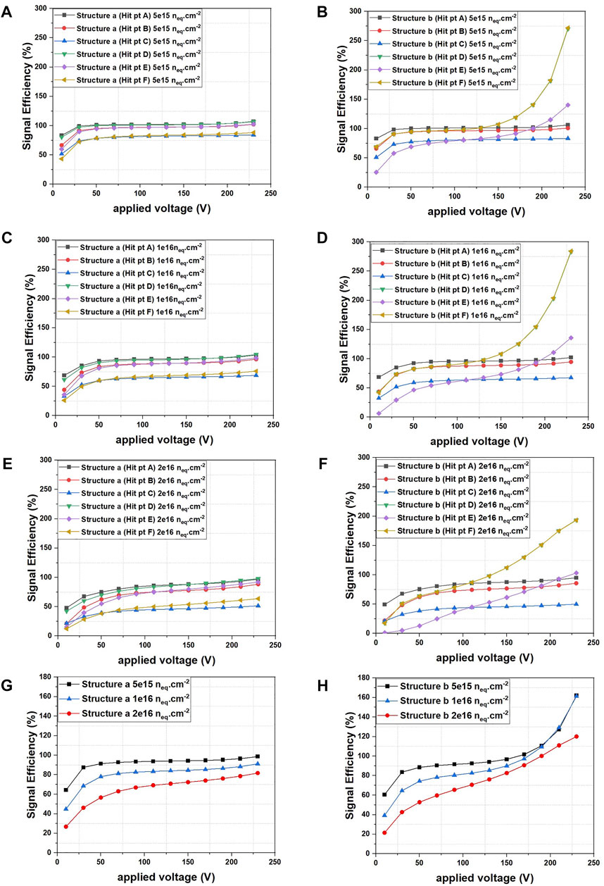
FIGURE 4. Simulated signal efficiency vs. applied voltage at different irradiation fluences: existing device for different hit points at (A) 5 × 10¹⁵neqcm−2, (C) 1 × 10¹⁶neqcm−2, and (E) 2 × 10¹⁶neqcm−2; proposed device for different hit points at (B) 5 × 10¹⁵neqcm−2, (D) 1 × 10¹⁶neqcm−2, and (F) 2 × 10¹⁶neqcm−2; average values at different fluences for (G) existing device and (H) proposed device.
The mean signal efficiency (average of values for hit points A–F) as a function of voltage at different fluences is shown in Figures 4G,H. As expected from previous plots, results are similar in the low voltage range, with relatively high signal efficiency, whereas the signal efficiency in the modified design is boosted by charge multiplication at larger voltage.
Results confirm that the proposed design modification has a good potential, but also some drawbacks. The electric field distribution is less uniform than in the existing design, and this might impact on the timing resolution, as also suggested by the comparison of the current signal transients. While an accurate estimate of the timing is not possible with the available data, a comparison of the Ramo maps with those obtained from a 3D pixel with columnar electrodes [4] suggests that better performance should anyway be obtained with the proposed design, making it appealing for several applications.
After irradiation up to 2 × 10¹⁶ neq/cm2, the proposed design is comparable to the existing one in terms of signal efficiency and superior to 3D pixels with columnar electrodes of similar inter-electrode distance [21]. Moreover, the electric field non-uniformity also impacts on the signal efficiency at high voltage: in particular, charge multiplication effects are position dependent and actually stronger in the boundary region between adjacent pixels. Another consequence of the close proximity between n+ and p+ trenches in adjacent pixels is probably an increased charge sharing. This should be carefully studied as a function of the trench dimensions, a topic that is beyond the purpose of this first proof of concept.
The raw data supporting the conclusion of this article will be made available by the authors, without undue reservation.
The manuscript was written by AB and G-FDB. All authors reviewed it.
This work was supported by the Italian National Institute for Nuclear Physics (INFN), 5th Scientific Commission (CSN5) with Project TIMESPOT; it also received funding from the European Union’s Horizon 2020 Research and Innovation programme under GA no. 101004761, and the Algerian Directorate General for Scientific Research and Technological Development (DGRSDT).
The authors declare that the research was conducted in the absence of any commercial or financial relationships that could be construed as a potential conflict of interest.
All claims expressed in this article are solely those of the authors and do not necessarily represent those of their affiliated organizations, or those of the publisher, the editors and the reviewers. Any product that may be evaluated in this article, or claim that may be made by its manufacturer, is not guaranteed or endorsed by the publisher.
Fruitful discussions with Dr. M. Boscardin and Dr. S. Ronchin (FBK, Trento) are warmly acknowledged.
1. Apollinari G, Bruening O, Nakamoto T, Rossi L. High-luminosity Large Hadron Collider (HL-LHC): Preliminary Design Report. CERN Yellow Rep (arXiv:2202.10271v1) (2015). doi:10.2172/1365580
2. Abada A, Abbrescia M, Abada A, Abbrescia M, Abdus Salam SS, Abdyukhanov I, et al. Fcc Physics Opportunities: Future Circular Collider Conceptual Design Report - Volume 1. Eur Phys J C (2019) 79:474. doi:10.1140/epjc/s10052-019-6904-3
3. Cartiglia N, Arcidiacono R, Ferrero M, Mandurrino M, Sadrozinski HFW, Sola V, et al. Timing Layers, 4- and 5-dimension Tracking. Nucl Instr Methods Phys Res Section A: Acc Spectrometers, Detectors Associated Equipment (2019) 924:350–4. doi:10.1016/j.nima.2018.09.157
4. Anderlini L, Aresti M, Bizzeti A, Boscardin M, Cardini A, Dalla Betta G-F, et al. Intrinsic Time Resolution of 3d-Trench Silicon Pixels for Charged Particle Detection. J Inst (2020) 15:P09029. doi:10.1088/1748-0221/15/09/p09029
5.The European Committee for Future Accelerators Detector R&D Roadmap Process Group. The 2021 ECFA Detector Research and Development Roadmap (CERN) (2021). doi:10.17181/CERN.XDPL.W2EX
6. Parker SI, Kenney CJ, Segal J. 3D - a Proposed New Architecture for Solid-State Radiation Detectors. Nucl Instr Methods Phys Res Section A: Acc Spectrometers, Detectors Associated Equipment (1997) 395:328–43. doi:10.1016/s0168-9002(97)00694-3
7. Parker S, Kok A, Kenney C, Jarron P, Hasi J, Despeisse M, et al. Increased Speed: 3D Silicon Sensors; Fast Current Amplifiers. IEEE Trans Nucl Sci (2011) 58:404–17. doi:10.1109/tns.2011.2105889
8. Kramberger G, Cindro V, Flores D, Hidalgo S, Hiti B, Manna M, et al. Timing Performance of Small Cell 3D Silicon Detectors. Nucl Instr Methods Phys Res Section A: Acc Spectrometers, Detectors Associated Equipment (2019) 934:26–32. doi:10.1016/j.nima.2019.04.088
9. Betancourt C, De Simone D, Kramberger G, Manna M, Pellegrini G, Serra N. Time Resolution of an Irradiated 3D Silicon Pixel Detector. Instruments (2022) 6:12. doi:10.3390/instruments6010012
10. Kenney CJ, Parker S, Walckiers E. Results from 3-D Silicon Sensors with wall Electrodes: Near-Cell-Edge Sensitivity Measurements as a Preview of Active-Edge Sensors. IEEE Trans Nucl Sci (2001) 48:2405–10. doi:10.1109/23.983250
11. Montalbano A, Bassignana D, Li Z, Liu S, Lynn D, Pellegrini G, et al. A Systematic Study of BNL׳s 3D-Trench Electrode Detectors. Nucl Instr Methods Phys Res Section A: Acc Spectrometers, Detectors Associated Equipment (2014) 765:23–8. doi:10.1016/j.nima.2014.03.066
12. Mendicino R, Kok A, Koybasi O, Povoli M, Summanwar A, Dalla Betta G-F. Characterization of SINTEF 3D Diodes with Trenched-Electrode Geometry before and after Neutron Irradiation. J Inst (2020) 15:C02023. doi:10.1088/1748-0221/15/02/c02023
13. Mendicino R, Forcolin GT, Boscardin M, Ficorella F, Lai A, Loi A, et al. 3D Trenched-Electrode Sensors for Charged Particle Tracking and Timing. Nucl Instr Methods Phys Res Section A: Acc Spectrometers, Detectors Associated Equipment (2019) 927:24–30. doi:10.1016/j.nima.2019.02.015
14. Forcolin GT, Boscardin M, Ficorella F, Lai A, Loi A, Mendicino R, et al. 3D Trenched-Electrode Pixel Sensors: Design, Technology and Initial Results. Nucl Instr Methods Phys Res Section A: Acc Spectrometers, Detectors Associated Equipment (2020) 981:164437. doi:10.1016/j.nima.2020.164437
15. Lai A, Anderlini L, Aresti M, Bizzeti A, Cardini A, Dalla Betta G-F, et al. First Results of the Timespot Project on Developments on Fast Sensors for Future Vertex Detectors. Nucl Instr Methods Phys Res Section A: Acc Spectrometers, Detectors Associated Equipment (2020) 981:164491. doi:10.1016/j.nima.2020.164491
16. Bellora A, Borgato F, Boscardin M, Brundu D, Cardini A, Cossu G, et al. 10 Ps Timing with 3D Trench Silicon Pixel Sensors. In: 15th Pisa Meeting on Advanced Detectors (2022).
17. Dalla Betta GF, Boscardin M, Darbo G, Mendicino R, Meschini M, Messineo A, et al. Development of a New Generation of 3D Pixel Sensors for HL-LHC. Nucl Instr Methods Phys Res Section A: Acc Spectrometers, Detectors Associated Equipment (2016) 824:386–7. doi:10.1016/j.nima.2015.08.032
18. Boscardin S, Ferrari M, Ficorella F, Lai A, Mendicino R, Meschini M, et al. Advances in 3D Sensor Technology by Using Stepper Lithography. Front Phys (2021) 9:625275. doi:10.3389/fphy.2020.625275
19. Benkechkache MA, Latreche S, Ronchin S, Boscardin M, Pancheri L, Dalla Betta GF. Design and First Characterization of Active and Slim-Edge Planar Detectors for FEL Applications. IEEE Trans Nucl Sci (2017) 64:1062–70. doi:10.1109/tns.2017.2672745
20. Folkestad Å, Akiba K, van Beuzekom M, Buchanan E, Collins P, Dall’Occo E, et al. Development of a Silicon Bulk Radiation Damage Model for Sentaurus Tcad. Nucl Instr Methods Phys Res Section A: Acc Spectrometers, Detectors Associated Equipment (2017) 874:94–102. doi:10.1016/j.nima.2017.08.042
21. Boughedda A, Lakhdara M, Latreche S, Mendicino R, Dalla Betta G-F. Comparing different bulk radiation damage models in tcad simulations of small-pitch 3D si sensors. J Inst (2021) 16:C10006. doi:10.1088/1748-0221/16/10/c10006
22. Ramo S. Currents Induced by Electron Motion. Proc IRE (1939) 27:584–5. doi:10.1109/jrproc.1939.228757
Keywords: silicon radiation detectors, 3D sensors, fabrication technology, radiation hardness, timing, TCAD
Citation: Boughedda A, Latreche S, Lakhdara M and Dalla Betta G-F (2022) A Modified 3D-Trench Pixel Detector: Proof of Concept by TCAD Simulations. Front. Phys. 10:957089. doi: 10.3389/fphy.2022.957089
Received: 30 May 2022; Accepted: 15 June 2022;
Published: 07 July 2022.
Edited by:
Giovanni Verzellesi, University of Modena and Reggio Emilia, ItalyReviewed by:
Geetika Jain, TRIUMF, CanadaCopyright © 2022 Boughedda, Latreche, Lakhdara and Dalla Betta. This is an open-access article distributed under the terms of the Creative Commons Attribution License (CC BY). The use, distribution or reproduction in other forums is permitted, provided the original author(s) and the copyright owner(s) are credited and that the original publication in this journal is cited, in accordance with accepted academic practice. No use, distribution or reproduction is permitted which does not comply with these terms.
*Correspondence: Gian-Franco Dalla Betta, Z2lhbmZyYW5jby5kYWxsYWJldHRhQHVuaXRuLml0
Disclaimer: All claims expressed in this article are solely those of the authors and do not necessarily represent those of their affiliated organizations, or those of the publisher, the editors and the reviewers. Any product that may be evaluated in this article or claim that may be made by its manufacturer is not guaranteed or endorsed by the publisher.
Research integrity at Frontiers
Learn more about the work of our research integrity team to safeguard the quality of each article we publish.