 Jiali Wu
 Runze Qi*
95% of researchers rate our articles as excellent or good
Learn more about the work of our research integrity team to safeguard the quality of each article we publish.
Find out more
ORIGINAL RESEARCH article
Front. Phys. , 01 September 2022
Sec. Optics and Photonics
Volume 10 - 2022 | https://doi.org/10.3389/fphy.2022.933301
This article is part of the Research Topic High-precision EUV and X-ray Optics for Advanced Photon Source Facilities View all 10 articles
The Ne VII line is an intense solar line emitted from the solar transition region located at 46.5 nm with a temperature of approximately 0.5 MK. The observation of a Ne VII line is important to deepen the understanding of solar physics. For observing the Ne VII line at 46.5 nm, we have proposed a narrowband Sc/Si multilayer that could avoid the other solar emission lines going to the observatory instrument. In this article, Sc/Si multilayers with a Sc thickness ratio of 0.35 (conventional design) and 0.65 (narrowband design) were deposited. The microstructures of both multilayers were measured by grazing incidence X-ray reflectometry, X-ray diffraction, and transmission electron microscopy. The results showed that the interdiffusion at the Si-on-Sc interface was more significant than that at the Sc-on-Si interface in both multilayer. Compared with the conventional multilayer, the narrowband multilayer had a thinner Si-on-Sc interface width. The measured reflectivity of the Sc/Si multilayer with a Sc thickness ratio of 0.65 was 37.9% at 45.5 nm with a near-normal incident angle of 4.60°. The bandwidth was 3.68 nm, which is narrow enough to observe the Ne VII solar line.
The solar transition region (TR) is a highly dynamic and nonuniform area between the chromosphere and corona [1]. Within this region, the temperature rapidly increases from roughly 0.02 to 0.8 MK, and the collisional and partially ionized plasma transforms into the less collisional and fully ionized plasma [2]. Emission lines from the TR cover approximately 40–160 nm in the extreme ultraviolet (EUV) and far ultraviolet (FUV) regions and contain physical information about the TR. In this spectral range, the imager and spectrograph are mostly used as observing devices [3–5]. An intense Ne VII emission line is formed at a temperature of 0.5 MK in the upper TR, which is important for monitoring solar eruptions [6]. The Ne VII line is located at 46.5 nm, and in order to realize the observation of this specific emission line, a solar EUV telescope operating at 46.5 nm has been proposed. Because the Ne VII line is surrounded by other solar emission lines, such as Mg VIII at 43.7 nm and the Ne V line at 48.0/48.3 nm, the EUV telescope requires a narrow spectral bandpass to avoid the influence of other lines [7]. The EUV telescope is designed using a Ritchey–Chrétien structure [8], and the narrow spectral bandpass for this instrument is achieved by multilayer mirrors. The telescope requires the bandwidth of multilayer mirror less than 4 nm to ensure performance, and the narrowband multilayer mirror can be achieved by optimizing the multilayer structure.
Sc/Si multilayers show a high reflectivity in the 35–50 nm wavelength range and have been used for 46.9 nm Ne-like Ar X-ray tabletop lasers, spectroheliography, and X-ray microscopy [9–11]. Yulin obtained the asymmetrical interface width as dSc-on-Si = 2.6 nm and dSi-on-Sc = 1.6 nm using the four-layer model (Sc/ScSi/Si/ScSi) [12]. At a Sc layer thickness ratio of 0.42 (ΓSc = dSc/d, where ΓSc represents the thickness ratio of the Sc layer, dSc represents the thickness of Sc, and d represents the d-spacing of the multilayer), the sample with a d-spacing of 25.45 nm had the highest reflectivity of 52% at 45.9 nm, and the bandwidth was 4.4 nm. At a constant d-spacing of 24.50 nm, the sample with ΓSc = 0.37 had the highest reflectivity. However, the microstructure of these multilayers with different ΓSc values has not been investigated. Gautier optimized the thickness of the top Si layer to 3.2 nm, whereby the reflectivity improved from 37 to 46% at 46 nm [13]. In the Sc/Si multilayer with a Sc ratio of 0.5, an asymmetrical interface was also found. The Si-on-Sc interlayer thickness was 2.5 nm, which was wider than the Si-on-Sc interlayer. Zhu indicated that the critical crystalline Sc layer thickness was about 5.68 nm [14]. However, previous work has usually focused on improving the reflectivity, and the Sc thickness ratio was between 0.37 and 0.5. The narrowband Sc/Si multilayer is important for 46.5 nm line imaging observations. Increasing the Sc layer thickness ratio is expected to achieve a narrow bandwidth of the Sc/Si multilayer, which is confirmed in the Mo/Si multilayer [15].
In this article, we designed the narrowband Sc/Si multilayer working at 46.5 nm. The narrowband Sc/Si multilayer with ΓSc = 0.65 and the conventional Sc/Si multilayer with ΓSc = 0.35 are deposited. These multilayers are characterized by different methods. The microstructures of both multilayers are measured by grazing incidence X-ray reflectometry (GIXR), X-ray diffraction (XRD), and transmission electron microscopy (TEM). The EUV reflectivity is measured by normal incidence reflectometry.
Taking into account the diffusion in periodic Sc/Si multilayers, a four-layer structure (Sc/ScSi/Si/ScSi) was set up for simulation, where ScSi was the diffusion interlayer at the Sc-on-Si interface and the Si-on-Sc interface. In the design, the density of the ScSi layers was assumed to be 3.30 g/cm3 [12]. The interlayer thickness at the Sc-on-Si and Si-on-Sc interfaces was set to 2.60 and 1.60 nm, respectively [16]. The surface and interface roughness were set to 0.30 nm. The reflectivity was computed at a near-normal incidence of 4.60°. To study the impact of ΓSc on the bandwidth and reflectivity of the Sc/Si multilayer, the reflectivity curves with different ΓSc values were calculated by the software IMD [17], as shown in Figure 1. Figure 1A shows the theoretical reflectivity of Sc/Si multilayers with a fixed d-spacing of 24.50 nm. With increasing the ratio from 0.35 to 0.75, the peak position increased from 45.5 nm to a longer wavelength of 48.9 nm. Meanwhile, the corresponding bandwidth and reflectivity decreased greatly, that is, the bandwidth decreased from 5.83 to 3.12 nm and the peak reflectivity decreased from 39.0 to 16.9%. It was demonstrated that increasing the Sc thickness ratio could effectively reduce the bandwidth of a Sc/Si multilayer while the reflectivity would drop. Figure 1B shows the theoretical reflectivity of Sc/Si multilayers with a d-spacing of 22.90–25.25 nm and a fixed working wavelength of 46.5 nm. When ΓSc was 0.65, the bandwidth decreased to less than 4.0 nm and the peak reflectivity was 31.8%. Based on these simulations, the Sc/Si multilayer with a d-spacing of 23.38 nm and ΓSc = 0.65 was opted to achieve a narrow bandwidth and relatively high reflectivity. In order to draw comparisons with this narrowband multilayer design, a conventional Sc/Si multilayer with ΓSc = 0.35 was designed. Schematics of the designed multilayer are depicted in Figure 2. Without considering the interlayer, the number of bilayers was 20.
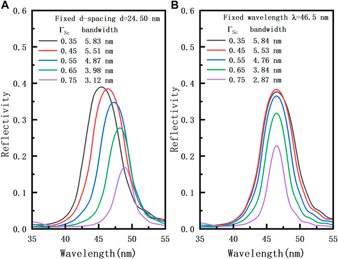
FIGURE 1. Theoretical reflectivity of the Sc/Si multilayers with different ΓSc values at a fixed d-spacing (A) and a fixed working wavelength of 46.5 nm (B).
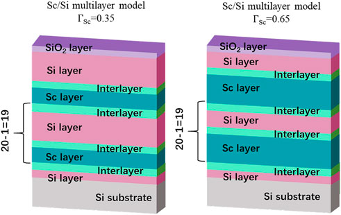
FIGURE 2. Schematic of the Sc/Si multilayer structures with ΓSc = 0.35 and ΓSc = 0.65.
According to the designed results, Sc/Si multilayers with ΓSc = 0.65 and ΓSc = 0.35 were deposited by direct-current magnetron sputtering. The base pressure was less than 7.0 × 10⁻⁵ Pa. High-purity Ar (99.999%) was used as the sputtering gas and the Ar pressure was maintained at 0.160 Pa during the deposition. The layer thickness was confined by varying the residence time of the substrate as it passed over each sputtering target. The sputtering power of the Sc and Si targets was 30 and 80 W, respectively. The multilayers were deposited on 20 × 20 mm2 super-polished silicon wafers with a root-mean-square roughness of 0.2 nm.
The structure of the samples was characterized by grazing incidence X-ray reflectometry (GIXR) with the 2theta-omega mode using an X-ray diffractometer (Bede, Durham, United Kingdom). The source was the Cu-Ka line at 0.154 nm. The GIXR measured curves were fitted by the software IMD using a two-layer model initially. However, compared with the intensity of the measured Bragg peaks, the simulated Bragg peaks had a lower intensity. According to previous literature, the measured curves were fitted with a four-layer model which took into account the Sc-Si mixtures at the interface. More information about the details of the multilayer structure is provided in Section 4.
Characterization of the crystallinity of multilayers was performed by X-ray diffraction (XRD, Bruker D8 Advance, Karlsruhe, GER). The detector scanned from 10° to 68° at a grazing incidence angle in the 2theta-omega mode. In this mode, the crystal plane parallel to the multilayer surface can be detected. The crystal phases can be obtained by matching the angular positions of the diffraction peaks with the powder diffraction file (PDF) of the International Center for Diffraction Data (ICDD). The average grain size perpendicular to the crystal phase direction was deduced by the Scherrer equation [18]:
where D is the average grain size,
In order to verify these results obtained by GIXR and XRD, the microstructures of multilayers were also investigated by transmission electron microscopy (TEM) using an FEI Talos F200X instrument (FEI, Hillsboro, OR, United States). It was equipped with a scanning TEM imaging with a nanoprobe for elemental contrast and an energy dispersive X-ray (EDX) spectrometer for elemental mapping. Selected area electron diffraction (SAED) measurements were used to characterize the crystallization of the multilayer. The profile of the layers along the growth direction was obtained by reading the gray value of the high-resolution TEM image using the software Digital Micrograph [19].
The EUV reflectivity of the Sc/Si multilayer with ΓSc = 0.65 was measured by Optics Beamline PM-1 at the BESSY-II facility. For the reflectivity measurement, the normal incidence monochromator was equipped with a grating of gl = 150 L/mm, and the beam stability was better than 0.1% [20]. The measurement was performed at an energy range of 22.3–33.5 eV (37.0–55.6 nm) and at a near-normal incidence angle of 4.60°.
The measured and fitted GIXR curves of Sc/Si multilayers with ΓSc = 0.35 and ΓSc = 0.65 are shown in Figure 3. The measured curves were fitted with a two-layer model, but the fitted curves could not fit nicely with the measured curves and did not present details of the interfaces. According to previous studies, Sc-Si mixtures would be formed at the interface of Sc/Si multilayers, which were considered as ScSi compounds. Thus, ScSi interlayers were added to the fitted model as the four-layer model (Sc/ScSi/Si/ScSi). The theoretical reflectivity peaks and intensities were in good agreement with the experimental reflectivity. At a grazing angle range from 0.4° to 1.0°, there was a little deviation between the measured and fitted curves. This was mainly caused by surface oxidation and contamination. This deviation will not affect the fitted thickness value of the interlayer. Table 1 presents the fitted structure of Sc/Si multilayers, including oxidation of the silicon surface layer. It clearly exhibits the interlayer asymmetry in both Sc/Si multilayers. For the Sc/Si multilayer with ΓSc = 0.35 and a d-spacing of 24.86 nm, the Si-on-Sc interlayer thickness was 2.96 nm, while the Sc-on-Si interlayer thickness was smaller at 1.30 nm. For the Sc/Si multilayer with ΓSc = 0.65 and a d-spacing of 23.26 nm, the Si-on-Sc interface thickness was 2.73 nm, while the Sc-on-Si interface thickness was 1.41 nm. In both multilayers, interdiffusion at the Si-on-Sc interface was wider than that at the Sc-on-Si interface. Interlayer asymmetry may be related to the crystallization of the Sc layers.
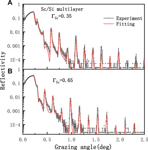
FIGURE 3. Measured GIXR and fitted results of Sc/Si multilayers with ΓSc = 0.35 (A) and ΓSc = 0.65 (B).
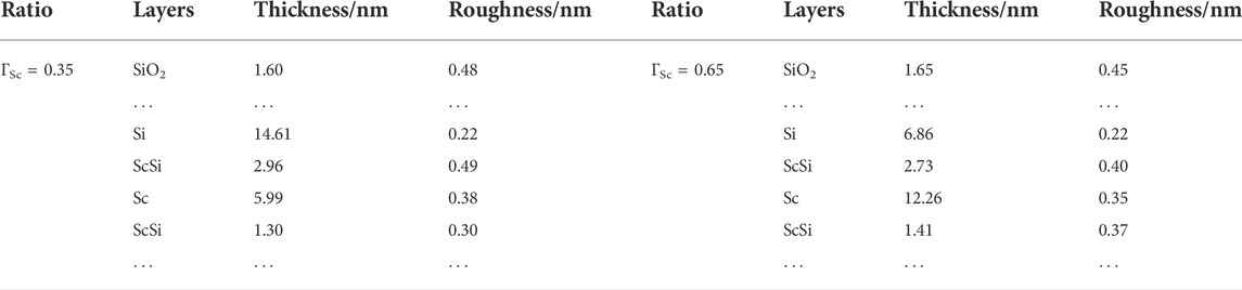
TABLE 1. Sc/Si multilayer fitted parameters deduced from GIXR measurements.
Figure 4 shows the diffraction curves of the Sc/Si multilayers obtained by XRD in symmetrical reflection mode. The angular positions and the bandwidths of diffraction peaks were determined by fitting the peaks with a Gaussian profile. According to the PDF reference, the two peaks identified at diffraction angles of approximately 34.01° and 35.65° correspond to the Sc (002) and (101) crystal planes of a hexagonal close-packed structure, respectively. These crystal phases were also proposed by Zubarev [21]. Compared with the Sc/Si multilayer with ΓSc = 0.35, the diffraction peaks of the Sc/Si multilayer with ΓSc = 0.65 were narrower, and the intensity was increased. It was also clearly observed that the crystallization of Sc (101) was stronger than that of Sc (002). According to the Scherrer formula, the average grain size of the crystal phases was calculated. For the Sc/Si multilayer with ΓSc = 0.35, the average grain sizes perpendicular to the Sc (002) and (101) crystal phases were 5.9 and 5.5 nm, which were close to the Sc layer thickness. For the Sc/Si multilayer with ΓSc = 0.65, the average grain sizes perpendicular to the Sc (002) and (101) crystal planes were increased to 7.6 and 8.6 nm, respectively.
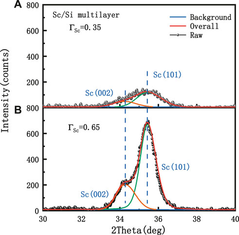
FIGURE 4. Measured XRD and fitted curves of Sc/Si multilayers with ΓSc = 0.35 (A) and ΓSc = 0.65 (B).
When the sputtered Si atoms were deposited on the crystalline Sc layer during the deposition, the crystal grains provided some diffusion channels and formed a thicker interlayer at the Si-on-Sc interface with Sc atoms [22]. When the sputtered Sc atoms were deposited on the amorphous Si layer, the underneath Si layer diffused into the growing Sc layer and formed another interlayer at the Sc-on-Si interface, which was thinner than that at the Si-on-Sc interface. Because the Sc layer was crystallized, while the Si layer was amorphous, the diffusion activities of Sc and Si atoms were different, which made the asymmetric interlayer at different interfaces.
The microstructures of the Sc/Si multilayers with ΓSc = 0.35 and ΓSc = 0.65 were measured by TEM and SAED; the measurements are shown in Figures 5A–F. Figures 5A and D are the bright-field TEM images and directly show the multilayer structure. The light and dark areas represent Si and Sc layers. A great number of grains obviously formed in the Sc layers. It was indicated that the Sc layers were partly crystallized. The thin gray area between the Sc and Si layers is Sc-Si mixtures, which can be observed more clearly in the high-resolution TEM images. Through Digital Micrograph software analysis, the d-spacings of the Sc/Si multilayer with ΓSc = 0.35 and ΓSc = 0.65 were 24.83 and 23.13 nm. This was almost consistent with the GIXR results. The bright-field high-resolution TEM images are shown in Figures 5B and E. The distribution of the Sc-Si mixtures and the different crystal orientations in the Sc layers are clearly observed. The average gray-value profile of the Sc/Si multilayers for one period was obtained from the same area later.
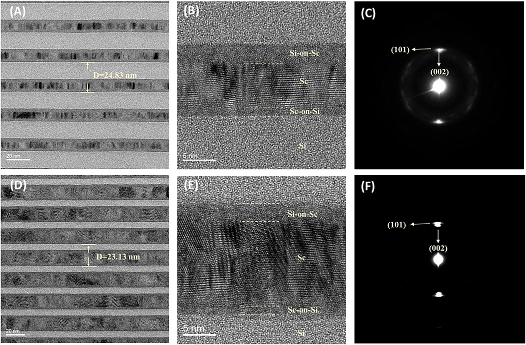
FIGURE 5. Bright-field TEM and SAED images of Sc/Si multilayers with ΓSc = 0.35 (A–C) and ΓSc = 0.65 (D–F).
The selected area electron diffraction (SAED) images are shown in Figures 5C and F. The bright diffraction spots were both aimed at Sc crystal phases. The Si layer and interlayers were in the amorphous phase. For the Sc/Si multilayer with ΓSc = 0.35, there were diffraction spots in the longitudinal direction, which corresponded to the Sc (002) and (101) crystal planes. For the Sc/Si multilayer with ΓSc = 0.65, the diffraction spots were brighter. It was illustrated that the crystallization of Sc (101) and (002) crystal phases was enhanced, and most of the Sc grains grew along the direction of the multilayer growth.
The average gray-value profiles of the Sc/Si multilayers obtained near the middle of the multilayer are shown in Figure 6. The Y axis represents the average reading gray values along the growing direction of the multilayer. The X axis represents the observed position along the direction of the multilayer growth, and 20% of the peak and valley difference in the selected area was defined as the interface width [23]. The peak value was chosen from the Si layer near the edge, and the valley value was chosen from the internal Sc layer. The purple arrows marked the selected peak and valley values in Figure 6. At the top of the gray-scale curve was the selected area in the TEM images in Figures 5B and E, which were rotated by 90°. For the Sc/Si multilayer with ΓSc = 0.35, the thickness of the interlayer at the Si-on-Sc and Sc-on-Si interfaces was approximately 3.00 and 1.51 nm, respectively. For the Sc/Si multilayer with ΓSc = 0.65, the thickness of the interlayer at the Si-on-Sc and Sc-on-Si interfaces was approximately 2.67 and 1.35 nm, respectively. The asymmetrical interlayers were close to the fitted values of the GIXR results. The diffusion of Si atoms was easier along the grain boundaries of the Sc layer when Si atoms were deposited on it. Thus, the Si-on-Sc interlayer thickness was wider than the Sc-on-Si interlayer thickness. In addition to the asymmetrical interlayer, it was also found that the Si-on-Sc interlayer thickness decreased from 3.00 to 2.67 nm when ΓSc increased to 0.65. This was mainly caused by the crystallization enhancement of the Sc layer. With the increase of the Sc layer thickness, the crystallization of Sc increased and the defect in the Sc layer decreased, which inhibited the diffusion of Si atoms.
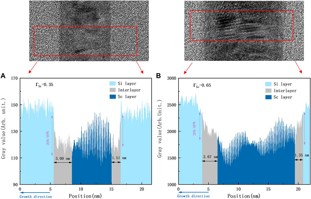
FIGURE 6. Gray-value profiles of Sc/Si multilayers with ΓSc = 0.35 (A) and ΓSc = 0.65 (B) derived from the selected area in the TEM images in Figures 5B and E (rotated by 90°).
Energy dispersive X-ray (EDX) spectroscopy was performed to study the depth distribution of chemical elements heavier than carbon [24]. Figure 7 shows the depth distribution of chemical elements of both Sc/Si multilayers. It obviously presents a periodic oscillation of the concentration of each element. The asymmetrical distribution of Si shown in Figure 7A is evidence of interfacial diffusion, but not concrete diffusion, due to the resolution. There was a small amount of O and Ar detected in both multilayers. This can be explained by Sc possessing active chemical properties, and it would react with the only remaining O during the deposition. Ar atoms were probably incorporated from the sputtering gas. Gautier also found that Ar impurities mainly existed in the Si layers through a Rutherford backscattering test [13]. The existence of Ar and O was one of the reasons affecting the reduced reflectivity.
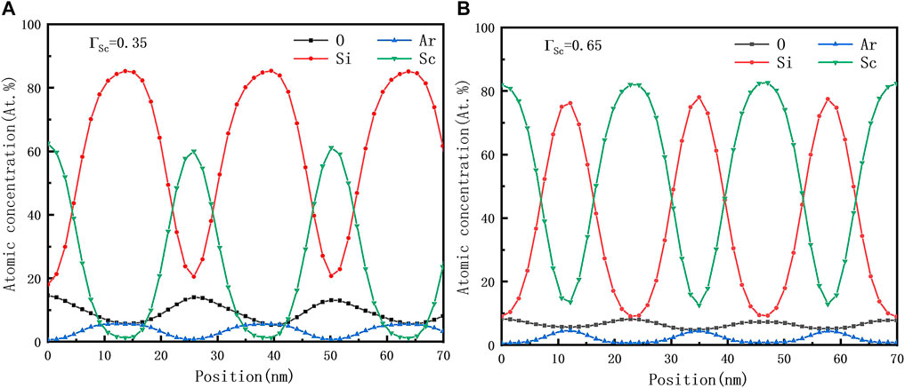
FIGURE 7. Depth distribution of the chemical elements of Sc/Si multilayers with ΓSc = 0.35 (A) and ΓSc = 0.65 (B). Sc/Si reflectivity measurement by synchrotron radiation.
The optical performance of the Sc/Si multilayer with ΓSc = 0.65 was performed by Optics Beamline PM-1 at the BESSY-II facility. We used the four-layer model with the parameters obtained from GIXR to calculate the reflectivity curve at a near-normal incidence angle of 4.60°. Figure 8 shows the measured reflectivity of the Sc/Si multilayer in comparison with the theoretical reflectivity. The experimental peak reflectivity was 37.9% at 45.5 nm with a 3.68 nm bandwidth at a near-normal incidence angle of 4.60°. The theoretical peak reflectivity of the Sc/Si multilayer with ΓSc = 0.35 was 40.1% based on the fitted structure. To the best of our knowledge, this is the narrowest measured bandwidth of Sc/Si multilayers obtained so far. However, there were differences between the measured and theoretical reflectivity. The wavelength of the measured peak reflectivity of the narrowband Sc/Si multilayer was 45.5 nm instead of 46.5 nm. This difference was due to uncertainties in the interlayer optical constants used in the calculation. These parameters might change in multilayers, especially in interlayers. The change in optical constant will affect the peak position of the reflectivity curve [25].
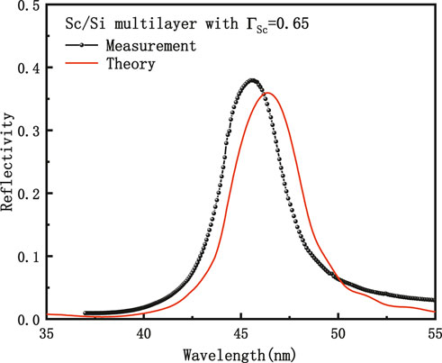
FIGURE 8. EUV reflectivity of the Sc/Si multilayer with ΓSc = 0.65.
We studied the structure properties of the Sc/Si multilayer with ΓSc = 0.35 and ΓSc = 0.65 and further characterized the optical performance of the Sc/Si multilayer with ΓSc = 0.65. The GIXR measurement showed that the Sc-on-Si interlayer thickness was almost unchanged (∼1.4 nm), whereas the Si-on-Sc interlayer thickness decreased from 3.0 to 2.7 nm when ΓSc increased from 0.35 to 0.65. XRD measurements revealed that the Sc crystal phases were mainly Sc (002) and (101). This was consistent with SAED measurements. At the Si-on-Sc interface, the diffusion between Sc and Si was reduced by the increasing crystallization of Sc. In the EUV measurement, the peak reflectivity of the multilayer with ΓSc = 0.65 was 37.9% at 45.5 nm. The bandwidth was 3.68 nm, achieving the current narrowband requirement for observation.
The original contributions presented in the study are included in the article/Supplementary Material; further inquiries can be directed to the corresponding author.
RQ and ZW conceived and designed the research work. JW analyzed the data and wrote the manuscript. ZZ and ZW contributed to helpful discussions to research and modification of the article. All authors have read and agreed to the published version of the manuscript.
This research was funded by the National Natural Science Foundation of China (12003016, 12027810, U2032169), the Strategic Priority Research Program of the Chinese Academy of Sciences (No. XDA15018400), and the Users with Excellence Program of Hefei Science Center CAS (2020HCS-UE005).
The authors declare that the research was conducted in the absence of any commercial or financial relationships that could be construed as a potential conflict of interest.
All claims expressed in this article are solely those of the authors and do not necessarily represent those of their affiliated organizations, or those of the publisher, the editors, and the reviewers. Any product that may be evaluated in this article, or claim that may be made by its manufacturer, is not guaranteed or endorsed by the publisher.
1. Vernazza JE, Avrett EH, Loeser R. Structure of the solar chromosphere. III - models of the EUV brightness components of the quiet-sun. ApJS (1981) 45:635. doi:10.1086/190731
2. Tian H. Probing the solar transition region: Current status and future perspectives. Res Astron Astrophys (2017) 17:110. doi:10.1088/1674-4527/17/11/110
3. De Pontieu B, Title AM, Lemen JR, Kushner GD, Akin DJ, Allard B, et al. The interface region imaging spectrograph (IRIS). Sol Phys (2014) 289:2733–79. doi:10.1007/s11207-014-0485-y
4. Boerner P, Edwards C, Lemen J, Rausch A, Schrijver C, Shine R, et al. Initial calibration of the atmospheric imaging assembly (AIA) on the solar dynamics observatory (SDO). Sol Phys (2012) 275:41–66. doi:10.1007/s11207-011-9804-8
5. Wilhelm K, Curdt W, Marsch E, Schühle U, Jordan SD, Poland AI, et al. Sumer - solar ultraviolet measurements of emitted radiation. Sol Phys (1995) 162:189–231. doi:10.1007/BF00733430
6. Peter H, Judge PG. On the Doppler shifts of solar ultraviolet emission lines. ApJ (1999) 522:1148–66. doi:10.1086/307672
7. Del Zanna G, Bromage BJI, Landi E, Landini M. Solar EUV spectroscopic observations with SOHO/CDS: I. An in-flight calibration study. A&A (2001) 379:708–34. doi:10.1051/0004-6361:20011220
8. Cheimets P, Caldwell DC, Chou C, Gates R, Lemen J, Podgorski WA, et al. SDO-AIA telescope design. Proc Spie: Solar Phys Space Weather Instrumentation (2009) III:74380G. doi:10.1117/12.830594
9. Rocca J-J, Frati M, Benware B, Seminario M, Filevich J, Marconi M, et al. Capillary discharge tabletop soft X-ray lasers reach new wavelengths and applications. Comptes Rendus de l'Academie des Sci - Ser IV - Phys (2000) 1:1065–81. doi:10.1016/S1296-2147(00)01113-6
10. Seely JF, Uspenskii YA, Pershin YP, Kondratenko VV, VinogradovSkylab AV. Skylab 3600 groove/mm replica grating with a scandium-silicon multilayer coating and high normal-incidence efficiency at 38-nm wavelength. Appl Opt (2002) 41:1846. doi:10.1364/AO.41.001846
11. Chakrabarti S, Kimble R, Bowyer S. Spectroscopy of the EUV (350–1400 Å) nightglow. J Geophys Res (1984) 89:5660. doi:10.1029/JA089iA07p05660
12. Yulin SA, Schaefers F, Feigl T, Kaiser N Advances in Mirror Technology for X-ray, 5193 (2004). p. 155–63. doi:10.1117/12.505582 Enhanced reflectivity and stability of Sc/Si multilayersProc SPIEEUV Lithography, Laser Other Appl
13. Gautier J, Delmotte F, Bridou F, Ravet MF, Varniere F, Roulliay M, et al. Characterization and optimization of magnetron sputtered Sc/Si multilayers for extreme ultraviolet optics. Appl Phys A (2007) 88:719–25. doi:10.1007/s00339-007-4041-6
14. Zhu J, Zhang J, Jiang H, Zhu J, Zhu S, Li M, et al. Interface study on the effect of carbon and boron carbide diffusion barriers in Sc/Si multilayer system. ACS Appl Mater Inter (2020) 12:25400–8. doi:10.1021/acsami.0c03563
15. Lim YC, Westerwalbesloh T, Aschentrup A, Wehmeyer O, Haindl G, Kleineberg U, et al. Fabrication and characterization of EUV multilayer mirrors optimized for small spectral reflection bandwidth. Appl Phys A Mater Sci Process (2001) 72:121–4. doi:10.1007/s003390000723
16. Gautier J, Delmotte F, Roulliay M, Ravet M-F, Bridou F, Jerome A, et al. Performances and stability of Sc/Si multilayers with barrier layers for wavelengths around 46 nm. Proc Spie: Adv Opt Thin Films (2005) 5963:59630X. doi:10.1117/12.625030
17. Windt DL. IMD—software for modeling the optical properties of multilayer films. Comput Phys (1998) 12:360. doi:10.1063/1.168689
18. Shaw LL, Goberman D, Ren R, Gell M, Jiang S, Wang Y, et al. The dependency of microstructure and properties of nanostructured coatings on plasma spray conditions. Surf Coat Tech (2000) 130:1–8. doi:10.1016/S0257-8972(00)00673-3
19. Mitchell DRGDT. Electron diffraction software tools for DigitalMicrograph TM. Microsc Res Tech (2008) 71:588–93. doi:10.1002/jemt.20591
20. Feng Y, Huang Q, Zhuang Y, Sokolov A, Lemke S, Qi R, et al. Mo/Si lamellar multilayer gratings with high efficiency and enhanced resolution for the x-ray region of 1000-1700eV. Opt Express (2021) 29:13416. doi:10.1364/OE.422483
21. Zubarev EN. Reactive diffusion in multilayer metal/silicon nanostructures. Phys -Usp (2011) 54:473–98. doi:10.3367/UFNe.0181.201105c.0491
22. Pershyn YP, Zolotaryov A, Rocca JJ, Devizenko AY, Kondratenko VV, Artyukov IA, et al. Formation of periodic relief at Sc/Si multilayer surface under EUV laser irradiation. Proc Spie: Damage Vuv, Euv, X-ray Opt VI (2017) 10236:102360J. doi:10.1117/12.2267292
23. Feng J, Huang Q, Wang H, Yang X, Giglia A, Xie C, et al. Structure, stress and optical properties of Cr/C multilayers for the tender X-ray range. J Synchrotron Radiat (2019) 26:720–8. doi:10.1107/S1600577519001668
24. Huang Q, Liu Y, Yang Y, Qi R, Feng Y, Kozhevnikov IV, et al. Nitridated Ru/B4C multilayer mirrors with improved interface structure, zero stress, and enhanced hard X-ray reflectance. Opt Express (2018) 26:21803. doi:10.1364/OE.26.021803
Keywords: Ne VII line, Sc/Si, multilayer, narrowband, thickness ratio
Citation: Wu J, Qi R, Zhang Z and Wang Z (2022) Structural and optical properties of narrowband Sc/Si multilayer at 46.5 nm. Front. Phys. 10:933301. doi: 10.3389/fphy.2022.933301
Received: 30 April 2022; Accepted: 25 July 2022;
Published: 01 September 2022.
Edited by:
Hongchang Wang, Diamond Light Source, United KingdomReviewed by:
Anil Kumar Malik, Chaudhary Charan Singh University, IndiaCopyright © 2022 Wu, Qi, Zhang and Wang. This is an open-access article distributed under the terms of the Creative Commons Attribution License (CC BY). The use, distribution or reproduction in other forums is permitted, provided the original author(s) and the copyright owner(s) are credited and that the original publication in this journal is cited, in accordance with accepted academic practice. No use, distribution or reproduction is permitted which does not comply with these terms.
*Correspondence: Runze Qi, cXJ6QHRvbmdqaS5lZHUuY24=
Disclaimer: All claims expressed in this article are solely those of the authors and do not necessarily represent those of their affiliated organizations, or those of the publisher, the editors and the reviewers. Any product that may be evaluated in this article or claim that may be made by its manufacturer is not guaranteed or endorsed by the publisher.
Research integrity at Frontiers
Learn more about the work of our research integrity team to safeguard the quality of each article we publish.