
95% of researchers rate our articles as excellent or good
Learn more about the work of our research integrity team to safeguard the quality of each article we publish.
Find out more
ORIGINAL RESEARCH article
Front. Phys. , 14 July 2022
Sec. Radiation Detectors and Imaging
Volume 10 - 2022 | https://doi.org/10.3389/fphy.2022.929251
 Thomas Corradino1,2*
 G.-F. Dalla Betta1,2
 C. Neubüser2
 L. Pancheri1,2On behalf of the ARCADIA collaboration
Monolithic Active Pixel Sensors (MAPS) represent one of the most promising technologies for the next generation of radiation detectors. The ARCADIA project aims at the development of Fully Depleted (FD) MAPS employing a production process compatible with a 110 nm commercial CMOS technology. The first engineering run of the project included matrices of active pixels with embedded analog and digital frontend electronics and passive test structures such as passive pixel arrays, MOS capacitors and backside diodes. Although the produced samples were already characterized from the electrical point of view, a thorough study of the charge collection dynamics of the passive pixel arrays was still missing. In this paper we show the results of the dynamic characterization of a group of passive pixel arrays with different pixel pitches (50, 25 and 10 μm) and different pixel layouts. The tested samples have been illuminated from the backside with an infrared and a red laser with wavelengths equal to 1,060 nm and 660 nm, respectively. The pixel arrays have been mounted on a custom readout PCB connected to an external amplifier with 1 GHz bandwidth and the signals have been acquired through a fast digital oscilloscope. We employed both focused and unfocused laser spots to evaluate the change in the measured signal as a function of the laser spot position and the average response of the pixel arrays. An excellent agreement has been demonstrated by comparing the measured signals with the results of transient TCAD simulations and a time for 50% charge collection of 7.8, 4.2 and 2.6 ns has been predicted and experimentally validated in pixels with 50, 25 and 10 μm pitch, respectively.
Several R&D projects are currently involved with the development of MAPS and follow alternative approaches trying to meet the increasingly demanding requirements in terms of performances set by the new generation of High Energy Physics (HEP) experiments and novel space and medical applications, while reducing the overall cost of the detector system [1–3]. The upgrade of the ALICE inner tracking system (ITS) represents the first large scale (10 m2) example of the use of MAPS in HEP [4]. One of the main advantage of MAPS with respect to traditional hybrid detectors consists in the absence of the need for the bump bonding process, leading to a decrease in the assembly costs and avoiding any possible bonding related issue. On the other hand, the presence of the embedded electronics on the same silicon substrate of the sensing elements poses some challenges in the way the reverse bias voltage can be applied to reach the substrate full depletion and thus in the use of the drift mechanism for charge collection. The development of MAPS able to exploit drift as the main charge collection mechanism represents the evolution of the first detector generation employed in the ALICE ITS, where the charge collection was dominated by the slower diffusion mechanism [4, 5]. In addition to the faster charge collection, this new sensor technology shows an improved radiation hardness and thus becomes attractive also for other applications, which involve higher radiation doses [6, 7]. The limit on the maximum voltage, that can be applied from the chip frontside to reach the sensor substrate depletion, represents the main limitation of this technology preventing the full depletion of thick silicon substrates. Alternative approaches for the realization of FD MAPS have been proposed in [8, 9]. In the first case, the devices are fabricated using a HV-CMOS production process, that is able to grant a depletion depth of several hundreds of micrometers at the cost of a large pixel capacitance. In the latter case, monolithic sensors are produced following the Silicon On Insulator (SOI) concept, where two silicon layers, hosting the embedded electronics and the sensing elements, respectively, are connected through an interposed buried oxide layer. Even though the two silicon layers can be optimized independently and thick high resistivity silicon layers can be properly depleted, the devices are affected by charge accumulation in the buried oxide layer. As a consequence, a specific design is needed to deal with this effect implying the use of a complex production process [10].
Trying to provide an alternative solution based on the approach proposed in [11], the goal of the ARCADIA project is the development of FD MAPS employing a commercial 110 nm CMOS production process, targeting medical imaging, HEP and space applications. Preliminary TCAD simulations have been performed in order to evaluate the possible sensor design solutions and select the most promising layouts in test structures [12–14]. The passive pixel arrays included in the first engineering run of the ARCADIA project have been characterized from the electrical point of view, extracting the operating voltage range and the pixel capacitance values for the different pixel pitches and layouts. We show in this work the results of the dynamic characterization of a group of passive pixel arrays with 50, 25 and 10 μm pixel pitch, that were backside illuminated with sub-nanosecond pulsed IR (1,060 nm) and red (660 nm) lasers, and we compare them with the results of transient TCAD simulations performed on single pixel 3D domains. In an analogous way, we compare the signals obtained from three pixel arrays with 50 μm pixel pitch and different pixel layouts with the corresponding TCAD simulation results to evaluate the layout effect on the charge collection speed. A focused laser spot has been employed to perform scans of the matrix areas and get information on the signal dependence on the laser spot position and we report an example of the obtained signal maps in the paper.
The paper is organized as follows: the TCAD simulation domains and physical models and the characteristics of the laser optical system used for the pixel array characterization are described in Section 2; in Section 3 we report a comparison of the experimental and simulation results and we show an example of the acquired signal maps; finally, we draw our conclusions in Section 4.
TCAD simulations were performed with Synopsys Sentaurus to investigate the main characteristics of the different pixel pitches and select the most promising pixel layouts in terms of operating voltage range, pixel capacitance and charge collection speed, and the results were reported in [12]. The different pixel layouts correspond to different sizes of the frontside p- and n-type implants, which impact significantly the pixel capacitance and the shape of the electric field in the region below the frontside surface and, as a consequence, the charge collection speed. To model the frontside implants we used in the simulations the doping profiles that were provided by the foundry.
In the transient simulations we employed 3D domains composed of a single pixel with 50, 25 or 10 μm pitch and a substrate thickness equal to 100 μm. A schematic cross section of a single pixel is reported in Figure 1A. Figure 1B represents an example of a 3D simulation domain with a pixel size of 50 μm. A n-type epitaxial layer with higher doping concentration (yellow region) grown on top of a high resistivity n-type silicon substrate is used to delay the onset of the punch through currents between the frontside and the backside p-type implants (blue regions). The red region represents the central n-type sensor node, which is surrounded by the pwell and deep pwell, shown in blue and light blue, respectively, where the conditioning electronics can be hosted. A schematic cross section of the domain extracted at the pixel center is reported in Figure 1C, where it is possible to observe the electric field map and the electric field lines for an applied voltage bias of −22 V. Looking at the shape of the field lines below the pwell, it is evident that the charges generated in the regions at the pixel edges follow a longer path to reach the collection electrode. This results in a slower charge collection speed for the charges generated farther from the pixel center and produces a tail in the signal. Decreasing the pixel size speeds up the charge collection as the electric field lines are straighter at the pixel edges and the electric field is higher. The pixel layout influences the charge collection dynamics as well since the electric field shape depends on the dimensions of the frontside p-type and n-type implants. In Section 3.1 we report the results of the TCAD simulations performed on single pixel domains with three different pixel pitches equal to 50, 25 and 10 μm and three layouts of the 50 μm pixel. The three considered layouts for the 50 μm pixel correspond to the pixel layout 1), which has a medium size of the n-type collection electrode, to the minimum capacitance layout 2) with a smaller nwell size and a larger pwell width, and finally to the layout with improved charge collection speed 3), which is similar to the layout 1 with a larger nwell width. Layouts 1 and 3 have the same area available for the in-pixel electronics, while in layout 2 the available area is slightly larger. The layout of the 25 μm pixels features smaller nwell and pwell sizes and, finally, the 10 μm pixels are characterized by the smallest n-type sensor node and pwell width.
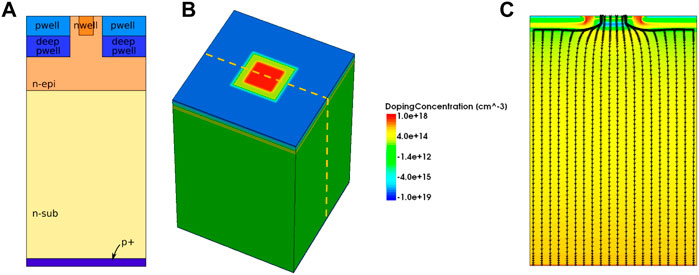
FIGURE 1. (A) Schematic cross section of an ARCADIA pixel (B) 3D TCAD simulation domain for the 50 μm pixel with layout 1. (C) Cross section of the domain showing the electric field together with the field lines in correspondence of the cut plane represented by the dashed orange line.
In the simulations we employed the Shockley Read Hall recombination model and we left the physical parameters describing the silicon substrate to the default values, except for the carrier lifetimes that were set to typical values for this technology. The transient simulations were performed to predict the sensor response to a monochromatic light source with a wavelength equal to 660 nm (red) or 1,060 nm (IR), that illuminates the sensor from the backside surface. The considered illumination window covers the whole backside pixel area and therefore the signal collected by the sensor node comprises the charge contributions generated in all pixel regions. This results in the presence of a signal tail representing the slower collection of the charges generated at the pixel edges. The optical generation was computed considering a photon absorption model described by Beer’s law. The optical generation profile was evaluated along the direction of propagation of the incident light beam inside the simulation domain. We considered an uniform and constant illumination inside the illumination window, covering the whole pixel area, and incident orthogonally to the backside surface. A Gaussian time dependence with a pulse duration of about 100 ps FWHM was specified for the light pulse.
The following bias scheme has been employed in the performed simulations: a voltage equal to 0.8 V is applied to the collection electrode, the pwell electrode represents the ground reference at 0 V and a negative voltage bias of −22V, or −32 V in the case of the 10 μm pitch pixel, is used to fully deplete the sensor substrate from the backside p+ electrode.
From the simulations we obtained the temporal evolution of the current collected by the sensor node and we compared these signals with the ones obtained experimentally from pixel arrays with same pixel pitch and layout.
The selected pixel layouts were included as test structures in the first engineering run as a group of passive pixel arrays with an area equal to 500 × 500 μm2. A preliminary set of measurements was performed at the probe station to determine experimentally from the IV characteristics the operating voltage range between the voltages needed to reach full depletion and the onset of the punch through. We extracted depletion voltages (Vdepl) in the order of -10 V and punch through voltages (VPT) around -20 V from the IV curves of the arrays with 50 and 25 μm pixel pitch. Higher values for Vdepl and VPT equal to −24 V and −30 V were obtained for the matrix with 10 μm pixels. CV measurements were performed as well to estimate the pixel capacitance and compare them with simulation results. The preliminary results of the electrical characterization of the passive pixel arrays are reported in [15]. Table 1 contains the measured full depletion and punch-through voltages and the pixel capacitance in full depletion condition extracted from TCAD simulations for an applied nwell voltage of 0.8 V.
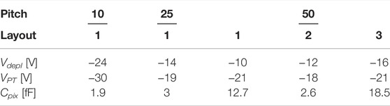
TABLE 1. Experimental full depletion (Vdepl) and punch-through (VPT) voltages and simulated pixel capacitance (Cpix) for the considered pixel pitches and layouts.
Once the operating voltage ranges were assessed, proving the proper functionality of the chips, we bonded the passive pixel arrays on custom passive PCBs through wire bonding to enable the sensor characterization in the optical setup shown in Figure 2. The setup is composed of an optical system, where the laser spot position can be controlled along the three principal axis directions. In particular, two stepper motors move the spot on the plane parallel to the focal plane and the motion in the third direction can be manually controlled with a maneuvering screw. A metal box shields the board with the tested sample and the external commercial amplifier from the electromagnetic noise. All the measurements are performed in a darkened box to suppress the noise due to the environmental light.
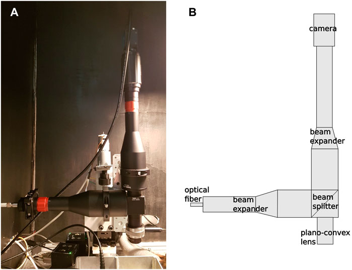
FIGURE 2. (A) Laser focusing system with coaxial camera that enables the identification of the laser spot position and the acquisition of pictures of the tested samples. (B) Laser focusing system simplified scheme.
The optical test signal is provided by a laser diode with a pulse width of 100 ps (FWHM) for the IR and 350 ps for the red laser. The laser light is launched into the focusing system from a single-mode optical fiber coupled to an achromatic collimator. The light then travels to a 2 inches beam expander followed by a 90–10 beam splitter crystal. From the beam splitter, 90% of the light goes to a plano-convex lens with a focal length of 100 mm and reaches the focal plane where the sensor surface is placed. Pictures of the tested sample can be acquired by a camera, coaxial with the optical column, with tunable focal length and equipped with a beam expander with visible light coating. A commercial charge amplifier (MiniCircuits ZFL-1000LM) with 23 dB gain and 1 GHz bandwidth is connected to the PCB and the amplified signal is acquired with a Tektronix Mixed Domain Oscilloscope with 1 GHz bandwidth (Tektronix MDO3102).
The sensors are backside illuminated through a hole in the holder PCBs with either a focused or an unfocused laser spot. In the first case, the charge generation is confined within a small silicon volume, since we estimated a laser spot diameter in the order of 10 μm at FWHM. This enables the evaluation of the pixel response as a function of the laser spot position performing scans over the pixel matrices. In the latter case, the light covers most of the matrix area and thus we obtain a signal that is the sum of the contributions related to collection of the charges generated in different positions over the whole pixel area. We use a motor step size of 10 μm or 5 μm in the scans, depending both on the resolution and total size of the observed device area.
An unfocused IR laser spot was used to obtain the response of a significant portion of the pixel matrix, providing a uniform signal generation within the area of each pixel. According to TCAD simulations, the fastest signal component is due to the collection of the charges generated in the region below the n-type sensor node. On the contrary, the charges generated at the edge between two adjacent pixels and at the corner among four pixels represent the slower contribution associated to the signal tail. The tested devices come from a wafer with a silicon substrate thickness of 100 μm and were compared with the results of simulations. In order to investigate the effect of the applied reverse bias voltage (Vbias) on the signal evolution, we performed measurements on the pixel matrices varying Vbias in a voltage range that starts below Vdepl and ends above VPT. The punch through voltage does not represent an absolute limit to the applicable bias voltage since the punch through current is still in the nA range with a Vbias exceeding VPT by several volts [15]. For this reason, we can apply a voltage higher than VPT while still granting a low power consumption for the detector.
Figure 3 represents the variation of the signal acquired from a pixel array with 50 μm pitch and layout 1 as a function of the applied Vbias. Looking at the figure, it is possible to observe that an increase in the applied bias voltage leads to a faster signal with a shift of the signal peak position to an earlier time instant, a decrease in the signal tail amplitude and a growth of the signal maximum peak amplitude. The observed trend confirms the expected behavior, showing a faster charge collection in the presence of a stronger electric field related to higher voltage bias. The increasing initial slope of the signal results from the higher electric field at the backside junction, which accelerates the charges generated in that region stronger than the ones closer to the collection node.
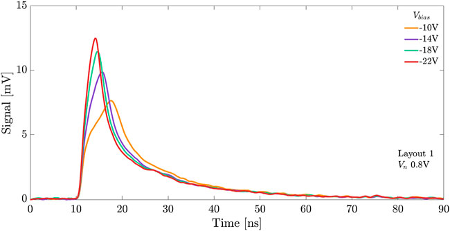
FIGURE 3. Measured signals for the pixel array with 50 μm pixels and layout 1 for different Vbias.
A comparison of the experimental signals with the ones obtained from TCAD simulations is reported in Figure 4 for the pixel arrays with 50 μm pitch and the three considered layouts (1, 2 and 3). The signals are normalized with respect to their maximum peak value to obtain a clearer comparison, highlighting the difference in their evolution. In the acquisition, the oscilloscope bandwidth was limited to 250 MHz to reduce electronic noise and electromagnetic interference, after noticing that, for this pixel size, high frequency components have a minor effect on the signal shape. A digital low-pass filter is applied to the simulated signals to reproduce the 250 MHz limit of the oscilloscope bandwidth. Looking at the graph we can state that an excellent agreement is reached between the TCAD simulation results and the measured data, proving the reliability of the models adopted in the simulations. We can also notice that the different pixel layouts correspond to different signal dynamics, with faster charge collection for the layouts characterized by larger nwell and smaller pwell and deep pwell sizes. In fact, the results obtained for layouts 1 and 3 are very similar. In particular, the signal associated to layout 2, featuring the smallest capacitance, shows a different dynamic with respect to the other layouts, having a long tail with a signal still in the order of 10% of the peak amplitude after 80 ns from the laser pulse.
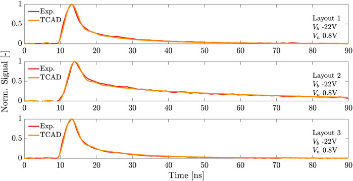
FIGURE 4. Comparison of the normalized signals obtained experimentally (red lines) and from TCAD simulations (orange lines) for three different layouts of the 50 μm pixels. The three subplots refer to the signals of layout 1, 2 and 3.
In an analogous way, Figure 5 includes a comparison of the signals observed for a decreasing pixel pitch. As expected, a smaller pixel size corresponds to a faster charge collection since the shape of the electric field is less affected by the presence of the pwell and deep pwell. Namely, the distance between the pixel collection nwells becomes shorter and therefore the charges generated at the boundary between adjacent pixels travel a shorter path in the regions with low electric field before reaching the collection electrodes. The signals included in the graph refer to the pixel matrices with pixel layout 1 for the three pixel sizes of 50, 25 and 10 μm. A higher backside bias, equal to −32 V, is applied to the 10 μm pixels as they have higher depletion and punch through voltages than the pixel arrays with 50 and 25 μm pixels, which instead show similar operating voltage ranges. We exploit the full bandwidth of the oscilloscope (1 GHz) in the measurements of the pixel arrays with 25 and 10 μm pitch to avoid the loss of the fast signal components at high frequency. In this case, a digital filter with 1 GHz cutoff frequency has been implemented and applied on the simulation results obtained for the corresponding pixel sizes.
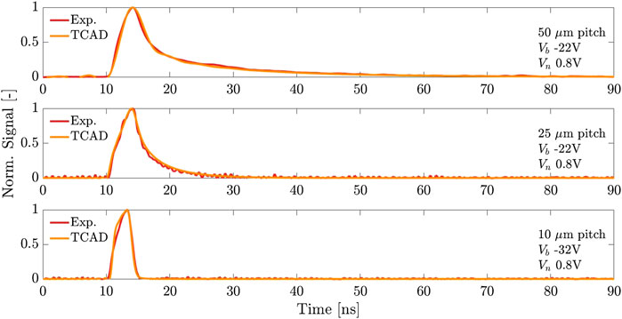
FIGURE 5. Comparison of the normalized signals obtained from the pixel array measurements (red lines) and the TCAD simulations (orange lines) for the devices with layout 1 and pixel pitch equal to 50 μm (top), 25 μm (middle) and 10 μm (bottom).
To obtain an estimate of the time needed to reach the collection of a specific fraction of the total amount of generated charges, we computed the integral of the acquired signals. As done previously, we compare the obtained signal integrals for the different pixel layouts of the 50 μm pixels (Figure 6) and for the three considered pixel pitches (Figure 7). Looking at Figure 6, we observe that the layouts 1 and 3 show similar charge collection dynamics in the first nanoseconds and only after the first 5 ns the latter starts having a slightly faster collection speed. On the contrary, the slower charge collection of pixel layout 2 appears clearly, requiring 27 ns to reach the collection of 50% of the generated charges instead of 7.8 and 6.6 ns for the standard and the fastest layout, respectively. As expected, the comparison of the signal integrals obtained from the pixel arrays with different pixel pitch (Figure 7) shows a reduced charge collection time for decreasing pixel size. The time needed for the collection of the 50% of the generated charges (t50) drops from 7.8 ns for the 50 μm pixel array, to 4.2 ns for the 25 μm pixels and finally to 2.6 ns for the 10 μm pixel matrix. This corresponds to an reduction of more than a factor 2 in the obtained t50 by decreasing the pixel size from 50 to 10 μm, and to the complete suppression of the signal tail after 5 ns.
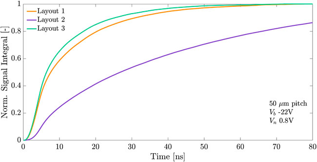
FIGURE 6. Comparison of the normalized signal integrals of the pixel arrays with 50 μm pixels and layout 1, 2 and 3.
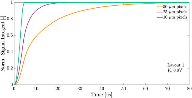
FIGURE 7. Comparison of the normalized signal integrals of the pixel arrays with layout 1 and 50, 25 or 10 μm pixel pitch.
Scans of the pixel arrays with 50 μm pitch have been performed using a focused laser spot to evaluate the variation of the pixel array signal as a function of the laser spot position. After noticing an undesired back reflection of the IR light due to the presence of the frontside metals, a red laser with 660 nm wavelength has been adopted for the matrix scans. The maps of the maximum signal peak and of the signal integrals obtained from scans of the pixel array with standard layout are shown as an example in Figure 8. A step size of 10 μm has been used in the scans of the whole matrix (Figure 8A), while a finer step of 5 μm has been employed to increase the position resolution in the scan of a portion of the matrix (Figure 8B). In the maps showing the maximum peak of the acquired signal, the higher values represented by the yellow spots correspond to the positions of the n-type sensor nodes and the light blue regions in between to the pwells at the pixel sides and corners. The presence of the n-guard ring around the pixel matrix affects the charge collection of the pixels at the matrix border. Namely, in the scan of the matrix corner it is possible to observe a decrease in the signal peak amplitude for the pixels at the borders of the matrix when the laser spot position is incident on their external side. The map of the integral of the measured signal is reported in Figure 8C as the amount of collected charges expressed in electrons for a considered integration time of 50 ns. Figure 8D shows the variation of the signal integral along a cross section taken in correspondence of a cut plane parallel to the x axis and passing in the matrix center. As expected, in the matrix boundary region, the signal integral depends on the laser spot position and decreases moving towards the outer half of the most external pixels due to the increasing amount of charges collected by the frontside n-guard ring. A complete extinction of the signal is observed when the laser spot has a distance larger than 50 μm from the edge of the pixel array. Excluding the pixels at the matrix boundary, the charge collection efficiency shows a good uniformity within the pixel array area with no significant variation when the laser spot is incident in different pixel positions.
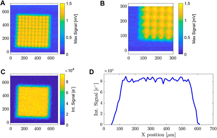
FIGURE 8. (A) Pixel signal maximum as a function of the laser spot position in a whole matrix scan with a motor step of 10 μm. (B) Pixel signal maximum as a function of the laser spot position in a matrix scan with a finer motor step of 5 μm. (C) Signal integral as a function of the laser spot position in a whole matrix scan with a motor step of 10 μm. (D) Signal integral as a function of the x coordinate along a cross section parallel to the x-axis.
First results of dynamic simulations and characterizations of passive pixel arrays with different pixel layouts and pixel pitches performed with an IR (1,060 nm) and a red (660 nm) laser have been presented. The overall dynamic performance of the pixel matrices have been evaluated employing an unfocused laser spot, large enough to cover a significant matrix area, in order to obtain a signal representing the contributions of the charge collection from different pixel regions. The measurements confirmed the simulated behavior, reproducing the dependence of the charge collection speed on pixel size and layout with excellent accuracy. From the signals of the pixel arrays we estimated a t50 in the order of 7.8, 4.2 and 2.6 ns for the three pixel pitches of 50, 25 and 10 μm. Finally, the matrix scans performed with a focused laser spot showed an uniform charge collection within the pixel arrays and enabled the evaluation of the influence of the frontside guard ring on the charge collection of the pixels at the matrix boundary. We will exploit the predictive power demonstrated by TCAD simulations to further optimize the pixel layout in different future application-specific designs.
The raw data supporting the conclusion of this article will be made available by the authors, without undue reservation.
CN, TC, and LP designed the pixel devices analyzed in this work. TC performed the TCAD simulations and the experimental measurements. G-FDB, CN and LP contributed to discussions and to the definition of the analysis methodology. TC wrote the manuscript. All authors reviewed it.
The research was carried on inside the framework of the ARCADIA project funded by the Istituto Nazionale di Fisica Nucleare, CSN5.
The authors declare that the research was conducted in the absence of any commercial or financial relationships that could be construed as a potential conflict of interest.
All claims expressed in this article are solely those of the authors and do not necessarily represent those of their affiliated organizations, or those of the publisher, the editors and the reviewers. Any product that may be evaluated in this article, or claim that may be made by its manufacturer, is not guaranteed or endorsed by the publisher.
We would like to thank LFoundry and Matteo Favaro for the support.
1. Snoeys W. CMOS Monolithic Active Pixel Sensors for High Energy Physics. Nucl Instr Methods Phys Res Section A Acc Spectrometers Detectors Associated Equipment (2014) 765:167–71. doi:10.1016/j.nima.2014.07.017
2. Wermes N. Pixel Detectors ... Where do we Stand? Nucl Instr Methods Phys Res Section A Acc Spectrometers Detectors Associated Equipment (2019) 924:44–50. doi:10.1016/j.nima.2018.07.003
3. Pancheri L, Giampaolo RA, Salvo AD, Mattiazzo S, Corradino T, Giubilato P, et al. Fully Depleted MAPS in 110-nm CMOS Process with 100-300-μm Active Substrate. IEEE Trans Electron Devices (2020) 67:2393–9. doi:10.1109/TED.2020.2985639
4. Mager M. ALPIDE, the Monolithic Active Pixel Sensor for the ALICE ITS Upgrade. Nucl Instr Methods Phys Res Section A Acc Spectrometers Detectors Associated Equipment (2016) 824:434–8. doi:10.1016/j.nima.2015.09.057
5. Snoeys W, Aglieri Rinella G, Hillemanns H, Kugathasan T, Mager M, Musa L, et al. A Process Modification for CMOS Monolithic Active Pixel Sensors for Enhanced Depletion, Timing Performance and Radiation Tolerance. Nucl Instr Methods Phys Res Section A Acc Spectrometers Detectors Associated Equipment (2017) 871:90–6. doi:10.1016/j.nima.2017.07.046
6. Schioppa EJ, Bates R, Buttar C, Dalla M, Van Hoorne JW, Kugathasan T, et al. Radiation Hardness Studies on a Novel CMOS Process for Depleted Monolithic Active Pixel Sensors. In: 2017 17th European Conference on Radiation and Its Effects on Components and Systems (RADECS), Geneva, Switzerland, 2-6 October 2017 (2017). p. 1–7. doi:10.1109/RADECS.2017.8696182
7. Pernegger H, Bates R, Buttar C, Dalla M, Hoorne JW, Kugathasan T, et al. First Tests of a Novel Radiation Hard CMOS Sensor Process for Depleted Monolithic Active Pixel Sensors. J Inst (2017) 12:P06008. doi:10.1088/1748-0221/12/06/p06008
8. Wang T, Rymaszewski P, Barbero M, Degerli Y, Godiot S, Guilloux F, et al. Development of a Depleted Monolithic CMOS Sensor in a 150 nm CMOS Technology for the ATLAS Inner Tracker Upgrade. J Inst (2017) 12:C01039. doi:10.1088/1748-0221/12/01/c01039
9. Arai Y, Ikegami Y, Unno Y, Tsuboyama T, Terada S, Hazumi M, et al. SOI Pixel Developments in a 0.15μm Technology. In: 2007 IEEE Nuclear Science Symposium Conference Record, Honolulu, HI, United States, 28 October - 3 November 2007 2 (2007). p. 1040–6. doi:10.1109/NSSMIC.2007.4437189
10. Asano M, Sekigawa D, Hara K, Aoyagi W, Honda S, Tobita N, et al. Characteristics of Non-irradiated and Irradiated Double SOI Integration Type Pixel Sensor. Nucl Instr Methods Phys Res Section A Acc Spectrometers Detectors Associated Equipment (2016) 831:315–21. doi:10.1016/j.nima.2016.03.095
11. Snoeys W, Plummer JD, Parker S, Kenney C. PIN Detector Arrays and Integrated Readout Circuitry on High-Resistivity Float-Zone Silicon. IEEE Trans Electron Devices (1994) 41:903–12. doi:10.1109/16.293300
12. Neubüser C, Corradino T, Dalla Betta G-F, De Cilladi L, Pancheri L. Sensor Design Optimization of Innovative Low-Power, Large Area FD-MAPS for HEP and Applied Science. Front Phys (2021) 9:639. doi:10.3389/fphy.2021.625401
13. De Cilladi L, Corradino T, Dalla Betta G-F, Neubüser C, Pancheri L. Fully Depleted Monolithic Active Microstrip Sensors: TCAD Simulation Study of an Innovative Design Concept. Sensors (2021) 21:1990. doi:10.3390/s21061990
14. Corradino T, Dalla Betta G-F, De Cilladi L, Neubüser C, Pancheri L. Design and Characterization of Backside Termination Structures for Thick Fully-Depleted MAPS. Sensors (2021) 21:3809. doi:10.3390/s21113809
Keywords: MAPS, CMOS, silicon radiation detectors, laser characterization, TCAD simulation
Citation: Corradino T, Dalla Betta G-F, Neubüser C and Pancheri L (2022) Charge Collection Dynamics of the ARCADIA Passive Pixel Arrays: Laser Characterization and TCAD Modeling. Front. Phys. 10:929251. doi: 10.3389/fphy.2022.929251
Received: 26 April 2022; Accepted: 23 June 2022;
Published: 14 July 2022.
Edited by:
Arianna Morozzi, Istituto Nazionale di Fisica Nucleare di Perugia, ItalyReviewed by:
Giovanni Ghione, Politecnico di Torino, ItalyCopyright © 2022 Corradino, Dalla Betta, Neubüser and Pancheri. This is an open-access article distributed under the terms of the Creative Commons Attribution License (CC BY). The use, distribution or reproduction in other forums is permitted, provided the original author(s) and the copyright owner(s) are credited and that the original publication in this journal is cited, in accordance with accepted academic practice. No use, distribution or reproduction is permitted which does not comply with these terms.
*Correspondence: Thomas Corradino, dGhvbWFzLmNvcnJhZGlub0B1bml0bi5pdA==
Disclaimer: All claims expressed in this article are solely those of the authors and do not necessarily represent those of their affiliated organizations, or those of the publisher, the editors and the reviewers. Any product that may be evaluated in this article or claim that may be made by its manufacturer is not guaranteed or endorsed by the publisher.
Research integrity at Frontiers
Learn more about the work of our research integrity team to safeguard the quality of each article we publish.