 Yun Chen
 Wei Huang
 Kelvin J. A. Ooi
 Wentao Zhang1*
- 1Guangxi Key Laboratory of Optoelectronic Information Processing, School of Optoelectronic Engineering, Guilin University of Electronic Technology, Guilin, China
- 2Department of Physics, Xiamen University Malaysia, Selangor Darul Ehsan, Malaysia
In this article, a novel graphene subwavelength waveguide coupler is designed based on the quantum control theory. Compared with metal surface plasmon polaritons (SPPs), graphene surface plasmon polaritons (GSPPs) have a smaller SPP wavelength and tunable properties. The dielectric load graphene plasmon waveguide (DLGPW) is used for designing to avoid the influence of the edge shape of the graphene nanoribbons on the waveguide mode. The coupling coefficient between the waveguides is calculated by using the coupled-mode theory (CMT). Due to the subwavelength properties of the graphene surface plasmons (GSP) and the robustness of the quantum control technique, our device is more compact and robust against perturbations of geometrical parameters under the premise of high transmission efficiency. The device we designed also has broadband characteristics, ranging from 30 THz to 40 THz, with high transmission efficiency when considering the transmission loss. We believe that our device will significantly contribute to integrated optics and photo-communication.
1 Introduction
Compared to the conventional surface plasmonic waveguides, such as spoof surface plasmon waveguide [1], graphene surface plasmon waveguide has promising properties, including tunability, extreme field confinement, and low propagation loss. Due to these characteristics, graphene surface plasmon waveguides are widely used to design ultrafast optical switches [2], ultrasensitive biosensors [3], and photodetectors [4]. Previous work design of the SPP waveguide on graphene only considers the coupling of parallel graphene sheets, such as Mach–Zehnder interferometers [5], tunable optical switches [6], and directional couplers [7]. The transmission efficiencies of the previous devices strongly depend on the geometrical parameters of the waveguide, such as the length of the device and the distance between waveguides. Accurate control of the geometric parameters of the device requires extremely high processing accuracy, which leads to an increase in fabricating costs, thus limiting the practical application of the device. Moreover, the performance of these devices is also susceptible to incident wavelengths, which usually works at a single frequency and lacks universality.
To solve the above-mentioned problems, a remarkable article proposed a vertical structure of a three-layered graphene waveguide coupler based on the Stimulated Raman Adiabatic Passage (STIRAP) [8], which is challenging to realize in actual applications due to the difficulty of fabricating multi-layer curved graphene plasmon waveguides [9]. Therefore, this article has explained the idea and design in fabricating the structure of in-plane asymmetric slightly curved three waveguide couplers, which is much easier to fabricate than a vertical structure.
In this article, we designed a robust and broadband in-plane graphene waveguide coupler based on STIRAP, which is a very effective technology for population transfer between quantum states and has been extensively studied in experiments and theoretical analysis in recent years [10]. The STIRAP technology can realize the complete population transfer of atoms from the initial state to the final state in a multi-level system and is widely used in many fields, such as laser cooling [11], cold atom manipulation [12], quantum information transfer [13, 14], and quantum computing [15, 16]. STIRAP has the advantage of high fidelity of intensity transmission and maintains the robustness to disturb the geometrical parameters. Most recently, there are many classical devices employing STIRAP, which have achieved broadband transmission and robustness with geometrical parameters [17–20].
According to the coupled-mode theory (CMT), the three-waveguide coupler can be analogized to a three-level atomic system with type lambda. The coupling equation of the graphene surface plasmons polaritons waveguide coupler can be analogized and written as the Schrödinger equation [9, 21]. The energy of GSPPs transfers from the input waveguide to the output waveguide through the intermediate waveguide, and the energy almost hardly remains in the intermediate waveguide. We used a dielectric-loaded graphene waveguide [22] for the design. Compared with the graphene nano-strip waveguide [23], there is no need to consider the influence of the edge shape of graphene as a zigzag or armchair. In this article, we used the equivalent refractive index method to analyze the mode profiles of the dielectric-loaded graphene waveguide, a typical and effective way for exploring the photonic and SP waveguide mode [24]. First, we calculated the relationship between the coupling length and the distance between two waveguides using the coupled-mode theory and compared it with the three-dimensional full-wave simulation results, which are in good agreement with each other. Then, by using CST Microwave Studio for simulation, the propagation process of GSPPs can be visually displayed. Furthermore, our article demonstrates the broadband characteristic of the device by simulating and analyzing the transmission efficiency and robustness of our device.
2 Model
In this article, we designed an asymmetric three-waveguide coupler, in which the middle waveguide is straight, and the two sides are slightly curved based on the STIRAP theory, as shown in Figure 1. The SPPs are excited at the left side of the input waveguide and reaches the output waveguide through the intermediate waveguide. We used CMT to calculate the relationship between the coupling strength and waveguide spacing, compared it with the simulation data, and then combined the STIRAP theory to obtain the critical geometric parameters of the device.
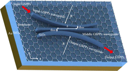
FIGURE 1. Schematic representation of the dielectric-loaded graphene plasmon waveguide coupler based on STIRAP. The dmin is the minimum distance between the input/output GSPP waveguide. The input and output waveguides are slightly curved, the radius of curvature is R, and the directions are opposite. In contrast, these waveguides are asymmetric, with a lateral mismatch δ between the two centers.
The input and output silica strips are slightly curved with the opposite curvature of radius R, and the mismatch distance between the centers of two curved waveguides is δ. dmin refers to the minimum spacing between the two curved silica strips and the middle. Previous studies have shown that the SPP mode remains unchanged in slightly curved graphene waveguides [25]. The geometry of the dielectric-loaded graphene plasmon waveguide coupler is shown in Figure 1. The substrate material of the device is silica with a dielectric constant of ɛr = 3.92; a dielectric strip with a width of w and height of h is deposited onto a graphene layer [26]. The relative permittivity of the strip is the same as the substrate, and the cladding is assumed to be air. We used the effective index method (EIM) [27] and CMT [28] to analyze the coupling between the waveguides and combine the STIRAP theory for the device design.
To analyze the optical properties of graphene, we applied the Kubo model [29] to describe the conductivity of graphene. The tunable optical conductivity of the monolayer graphene (σ(ω) = σintra(ω) + σinter(ω)) consists of intraband contribution (σintra(ω)) and interband contribution (σinter(ω)), which are defined by the following expressions [30]:
where e is the electron charge, and μ is the chemical potential of graphene. ℏ is the reduced Planck’s constant, and ω = 2πf is the radian frequency. τ is the relaxation time, and T is the Kelvin temperature. In simulation implementation, we assumed that the temperature is 300 K, the frequency range is 30–40 THz, the chemical potential is adjustable, and the relaxation time is 0.5 ps [6, 30–35].
We first used the effective index method (EIM) [27] to calculate the approximate effective refractive index of the dielectric-loaded graphene plasmon waveguide (DLGPW) as shown in Figure 2A. In the effective index method (Figure 2B), the dielectric strip serves as the core of a three-layered dielectric planar waveguide (Figure 2C). The refractive index of the core is independent of the width of the dielectric strip and is equal to the effective mode index of the TM mode in the planar graphene sheet sandwiched between the substrate and dielectric strip, which is written as [35]
where σ(ω) is the optical conductivity of graphene, c is the speed of light, and ɛ0 is the permittivity constant in vacuum; the relative permittivity values of the substrate ɛr1 and the dielectric strip ɛr2 are both 3.92. The refractive index of the cladding is equal to the effective mode index of the GSP mode (TM mode) in the planar graphene sheet sandwiched between the substrate and air and is expressed as [35],
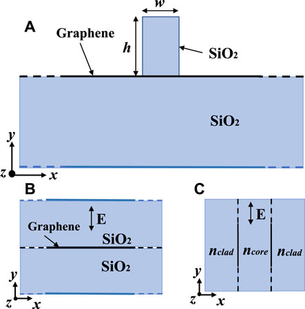
FIGURE 2. (A) Cross section in the main view of the single dielectric-loaded graphene plasmon waveguide structure. (B) Equivalent three-layered planar waveguide structure of DLGPW. (C) Equivalent three-layered planar waveguide structure based on EIM.
Then, by simple algebraic operation, the eigen equation of the equivalent dielectric planar waveguide for the m-th order guided TE mode is given as [35]
where w = 50 nm is the width of the dielectric strip, μclad = μcore = 1 is the relative permeability, k0 = ω/c is the vacuum wave number,
We calculated the mode profile of the waveguide and the coupling coefficient of the waveguide mode by employing the coupled-mode theory. In the optical waveguide theory, the expression of the waveguide mode can be assumed as [28]
where
Considering that the two planar waveguides are made of two slabs of widths w, separation 2a, and refractive index ncore, embedded in a medium of refraction index nclad, each of the waveguide modes is assumed to be a fundamental mode. Due to the gap between the waveguides, the light field outside the boundary of one waveguide can slightly overlap with the other waveguide. The coupled-mode theory is usually used to describe the weak coupling between two adjacent waveguides, and it has been verified in experiments.
According to the coupled-mode theory, the coupling coefficient between two adjacent waveguides is defined as follows [28]:
where n1 is the refractive index of waveguide 1. n2 is the refractive index of waveguide 2. n is the refractive index of the equivalent waveguide cladding. β1 and β2 are the propagation constants of the two waveguides, respectively. Since two adjacent waveguides have the same material and geometric parameters, n1 is equal to n2. Due to the symmetry of the waveguide mode profiles with the same refractive index, that is, u1(x) = u2(x), it is observed that the coupling coefficient between waveguide 1 and waveguide 2 (Ω12) is equal to the coupling coefficient between waveguide 2 and waveguide 1 (Ω21). Using the CMT to calculate the coupling coefficient between two parallel waveguides, the coupling length is calculated, and then, the results are verified by employing the full-wave simulation.
The CMT is used to calculate the coupling coefficient between two parallel waveguides, and the coupling length is given by Lc = π/2Ω [28]. The results of 3D full-wave simulation are consistent with the coupled-mode theory. The frequency in simulation and calculation is fixed at 35 THz, and the chemical potentials of graphene are taken as 0.6, 0.7, and 0.8 eV for simulation and calculation, respectively, and the results are in good agreement. In Figure 3, the solid line represents the theory results, and the discrete point represents the simulation results. The small illustration in the upper left corner of Figure 3 shows the cross-sectional configuration of the parallel waveguides. In the simulation, the dielectric strips on the graphene and substrate are both SiO2 with a relative permittivity of 3.92, the thickness of the substrate is 200 nm, the height and width of the parallel dielectric strips are h = 100 nm and w = 50 nm, respectively, and the spacing of parallel dielectric strips g varies uniformly in the range of 10–100 nm.
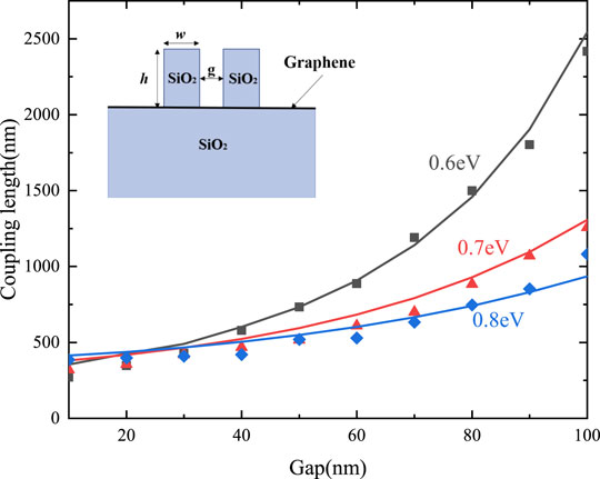
FIGURE 3. Coupling lengths of two parallel waveguides vary with the gap distance, when the chemical potential is 0.6e V (gray), 0.7 eV (red), and 0.8 eV (blue).
In Figure 3, we demonstrated that the coupling lengths exponentially increase (corresponding to the coupling strength exponential decrease) between the adjacent waveguides with the increase in the gap distance. The coupling strength increases with the increase in graphene chemical potential. According to Eqs 1, 2, when the chemical potential of graphene increases, the real part and the imaginary part of the conductivity of graphene increase correspondingly. The graphene conductivity is substituted into Eqs 3–5 to obtain nclad, ncore, and neff, respectively. We found that the refractive index of the waveguide core and cladding both decrease with the increase in graphene chemical potential, the effective refractive index of the waveguide decreases, and light is weakly confined, and coupling between the adjacent waveguides is enhanced. We also found that the coefficient before the integral term increases with the increase in graphene chemical potential by calculating Eq. 7. Therefore, as the chemical potential of graphene increases from 0.6 to 0.8 eV, the coupling strength between the adjacent waveguides increases.
The performance of a directional coupler that employs two parallel waveguide structures is susceptible to the geometrical parameters of the device, for example, the device length and distance between two adjacent waveguides. The three-waveguide coupler based on STIRAP can solve this issue with excellent robustness against perturbations of the device’s geometrical parameters in previous studies. The three-waveguide coupler can be an analogy to a three-level quantum system by employing STIRAP. The STIRAP analog in a three-WG directional coupler is already known in the area of quantum optics, both in theoretical derivation and experimental demonstration [8, 10, 12]. In the previous studies, the coupling equation of GSPPs can be described as Schrödinger-like Eq. 9
where a1(z), a2(z), and a3(z) are the power amplitudes of the corresponding waveguides, respectively, and Ω1(z) (Ω2(z)) is the coupling strength between the input and middle (middle and output) GSPP waveguides, and they can be calculated by the CMT. Since the three waveguides are made of the same material (with the same Fermi energy level), there is no detuning between these waveguides, so the diagonal elements of the Hamiltonian matrix in Eq. 8 are zero. We assumed that there is no coupling between the non-adjacent waveguides. The non-adiabatic Hamiltonian H is expressed as
According to the STIRAP theory, we should convert the non-adjacent base into an adiabatic base; the eigen values are V0 = 0;
where the mixing angle θ is given by tan θ = Ω1/Ω2. The adiabatic state set [ϕ+ ϕ0 ϕ−]† can be transferred from a non-adjacent set [a1 a2 a3]† with the rotation matrix R(t) as
Substituting the rotation matrix R(t) into the Schrödinger-like equation, Eq. 8 obtains the time-dependent Schrödinger-like equation in an adiabatic state and reads
where Ha is the adiabatic Hamiltonian, given by
Thus, if it satisfies the following adiabatic condition
According to the adiabatic following condition, we observed Ω2 ≫Ω1 in the initial state and Ω1 ≫Ω2 in the final state and
3 Results
In this example, the chemical potential of graphene is 0.7 eV, and the frequency is 35 THz. For the rest of the parameters of the waveguide, we chose the radius of curvature R = 3.6 μm, mismatch δ = 0.55 μm, and the minimum distance between the waveguides dmin = 0.02 μm. The device length was L = 1 μm, considering the propagation length [35] of the GSPPs Lp = λ0/[2πIm (neff)] ≈ 2.75 μm under the above-mentioned conditions. The parameters that are not specified are the same as the previous settings.
Figure 4 describes the distance variation between the input waveguide and the output waveguide through the intermediate waveguide with the propagation distance. The solid blue line represents the distance variation between the input waveguide and the intermediate waveguide, and the solid red line represents the distance variation between the output waveguide and the intermediate waveguide. The spacing of the input and output silica strip refers to the middle strip described by d1(z) and d2(z), which are given by
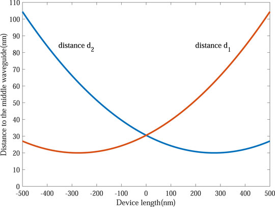
FIGURE 4. Distance between the input/output and middle waveguides.
According to the theory of STIRAP, the coupling strength between the input and middle (middle and output) waveguide is modeled as the Gaussian shape, as shown in Figure 5. By using the relationship of the coupling strength against the gap distance between the waveguides, the geometrical parameters of the device can be obtained by the functions of d1(z) and d2(z), which are described as the distance between the input and middle (middle and output) waveguide. We designed the geometric structure of our device based on the STIRAP theory, in which the coupling strength between two adjacent waveguides varies in the Gaussian shape, and sufficient overlapping is required. Figure 5 shows the distribution of the coupling strength function at different frequencies. Although the profiles of the coupling strength have changed, the adiabatic condition of the STIRAP process can still be satisfied. The visualization results of the energy transfer are shown in Figure 8.
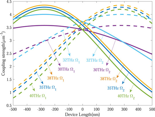
FIGURE 5. Coupling strengths distribution of the input (output) waveguide and middle waveguide at different frequencies.
By solving Eq. 8, we can obtain the SPP intensity transmission rate in Figure 6. Figure 6 demonstrates that our device can provide complete SPP energy transfer from the input to output GSPP waveguide in the ideal configuration without considering the loss. Furthermore, we considered the loss with the propagation of the GSPPs in our calculations with the imagery part of the propagation constant, and the energy of the GSPPs decays exponentially along with the increase in the propagation distance. In the lossy case, the transmission rate is still approaching 70% with the dashed lines in Figure 6. Therefore, our device can achieve complete GSPP energy transfer from the input to output GSPP waveguide.
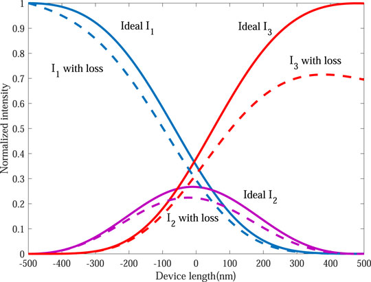
FIGURE 6. Population transfer in a three-waveguide coupler system.
4 Discussion
In this section, we analyzed the robustness and the broadband performance of our waveguide coupler. Now, we demonstrate the robustness of our device. First, the final transmission rate is defined as Pout/Pin, where Pout = |Eout|2, Pin = |Ein|2, and Ein (Eout) represent the intensity of the input (output) GSPPs. To demonstrate the robustness against the geometric parameters of our design, we varied the device length L (from 0.45 to 1.5 μm) and the radius of curvature R (from 1 to 4 μm), with the fixed dmin = 20 nm and mismatched δ = 550 nm, and the color map of the final transmission rate is shown as in Figure 7A. The radius of curvature R corresponds to the full width at half the maximum of the coupling strength function. When R increases, the distance between the waveguides becomes smaller. Since the coupling strength between the waveguides increases exponentially with the decrease in the distance, under the premise that other parameters are fixed, the coupling strength between the adjacent waveguides increases, while the maximum coupling strength remains unchanged. Therefore, the profiles of the coupling strength function broaden, and the full width at half the maximum of the coupling strength increases. From the results, if we choose the device length as the fixed value (for example, L = 1 μm), when the radius of curvature R varies roughly from 2.5 to 4 μm, the final transmission rate is still over 60%. Similarly, if we fix the radius of curvature R, the robustness of the device length can be described in the same way. Then, we calculated the final transmission rate by varying the minimum distance dmin (from 10 to 80 nm) and the mismatch δ(from 0 to 1000 nm) with the fixed length of the device L = 1 μm and the radius of curvature R = 3.6 μm, which is shown in Figure 7B. The minimum distance dmin between the adjacent waveguides corresponds to the maximum coupling strength between the adjacent waveguides. According to the coupled-mode theory (CMT), the coupling strength between the waveguides decreases exponentially as the distance between the waveguides increases. Hence, the minimum distance between the waveguides corresponds to the maximum coupling strength. The mismatch δ corresponds to the distance between the peaks of the coupling strength function Ω1 and Ω2. When the mismatch between the two coupling strength functions increases, the distance between the two coupling strength peaks increases. On the premise that other parameters are fixed, the overlap of the coupling strength decreases, and the coupling is insufficient. Conversely, when the mismatch between the two coupling strength functions decreases, the distance between the two coupling strength peaks decreases. On the premise that other parameters are fixed, the overlap of the coupling strength increases, and over-coupling may occur. Insufficient coupling or over-coupling will result in reduced transmission efficiency. From the results, we can conclude that the performance of our device is robust against the perturbations of the minimum distance dmin and the mismatch δ. For example, when the minimum distance between the input/output waveguide and middle waveguide dmin is fixed at 30nm, the mismatch between the input and output waveguide can vary roughly from 300 to 700 nm with a final transmission rate over 60%. The variation of these geometric parameters within a specific range can be considered as the disturbance of the two coupled Gaussian pulses in the STIRAP process. Due to the strong robustness of the system, it still has high transmission efficiency in the presence of disturbances.
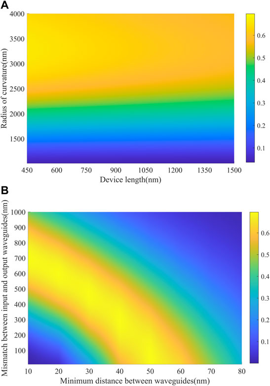
FIGURE 7. Robustness of the geometrical parameters and the calculations at 35 THz, 0.7 eV. (A) Final transmission rate against the device length and the radius of curvature, with fixed dmin = 20 nm and mismatch δ = 550 nm. (B) Final transmission rate against different minimum distances dmin and mismatch δ, with the fixed length of the device L = 1 μm and the radius of curvature R = 3.6 μm.
To visualize the characteristic broadband performance of our device, we carried out the full-wave simulations based on the geometric parameters derived by STIRAP combined with the coupled-mode theory. We used the plasmonic waveguide part of the MW and RF and OPTICAL modules in CST Microwave Studio for the simulation. The solver we used in the simulations is a frequency-domain solver. Open boundary conditions are set in all directions (corresponding to the perfectly matched layer). The waveguide port was used to excite the waveguide mode, and the polarization of the incident wave is transverse magnetic (TM) mode polarization. The size of the port is large enough to extend 150 nm in y directions (include y+ and y−) and 120 nm in x directions (include x+ and x−) with the graphene layer of the input waveguide as a reference, ensuring that the mode profile is not truncated. The graphene monolayer is treated as a thin film with the thickness t = 1 nm, which is the typical thickness in simulation [6, 30]. The permittivity of graphene can be defined as ɛ(ω) = 1 + iσ(ω)/ɛ0ω t, where ω is the radian frequency, ɛ0 is the vacuum permittivity, t is the thickness of the graphene layer, and σ(ω) = σintra(ω) + σinter(ω) is the optical conductivity of graphene [30]. The conductivity of graphene σ(ω) consists of intraband contribution σintra(ω) and interband contribution σinter(ω) defined as in Eqs 1, 2. The meshes are refined for more accurate results, the maximum mesh step is 10 nm, and the minimum mesh step is 0.2 nm in our setting.
We performed the simulations with different input frequencies to verify the performance of the device. The device we designed has good performance in the frequency band from 30 THz to 40 THz, as shown in Figure 8, which demonstrates the broadband characteristics of the device. When the frequency of the incident light is continuously increased from 30 THz to 40 THz, the graphene conductivity is calculated according to Eqs 1, 2. The real part and imaginary part of the graphene conductivity decrease with the increase in the frequency. When the incident frequency increases from 30 THz to 40 THz, the cladding refractive index, core refractive index, and effective refractive index of the equivalent waveguide increase, respectively, according to Eq. 3∼Eq. 5. Therefore, the effective refractive index of the waveguide increases, and the light is strongly confined. The distance between the input and middle (middle and output) waveguides is defined by d1(z)(d2(z)). According to Eqs 6, 7, if the function of the distance between the adjacent waveguides is unchanged, the coupling strength of the corresponding position between the waveguides will vary with the increasing frequency, so the coupling strength between the adjacent waveguides Ω1 and Ω2 will change (Figure 5).
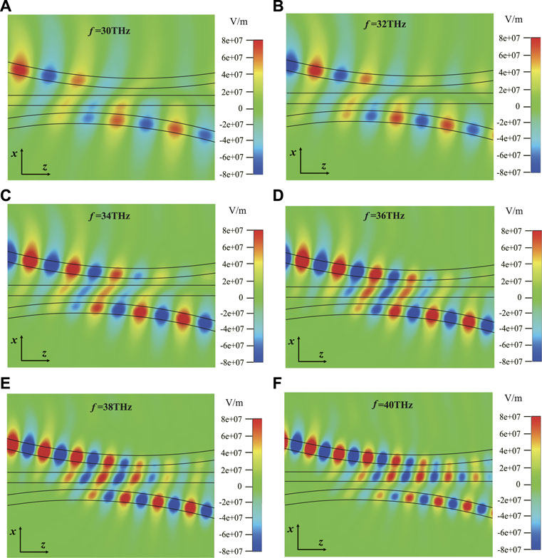
FIGURE 8. Full-wave simulation results of our device. The distributions of E-field on the y = 0 plane of our device based on simulation at different frequencies (A) 30 THz, (B) 32 THz, (C) 34 THz, (D) 36 THz, (E) 38 THz, and (F) 40 THz.
According to the adiabatic evolution conditions of the STIRAP process, Ω2 ≫Ω1 in the initial state, and Ω1 ≫Ω2 in the final state can still be satisfied, with the mixing angle θ changes from 0 to π/2 and the changing of θ being smooth. Therefore, the adiabatic evolution process of energy from the input waveguide to the output waveguide can be completed without the excitation of the middle waveguide. Consequently, the change in the incident frequency can be regarded as a perturbation to the profile of the coupling strength function. As long as the adiabatic evolution conditions are satisfied within a specific range of variation, high-fidelity adiabatic transmission can be achieved, thus realizing the broadband transmission.
Therefore, the varying geometric parameters and frequency ω change the two Gaussian shapes of coupling, Ω1 and Ω2. However, the theory of STIRAP makes sure that the system is very robust against the two varying Gaussian shapes. To sum up, our design is robust against varying the frequency and geometric parameters due to the coupling of STIRAP. The parallel configuration is sensitive to the perturbations of the excited frequency. There is a strong correlation between the transmission efficiency and coupling length for the parallel waveguides. The changes in the incident frequency will also change the coupling coefficient between the adjacent waveguides, thus changing the coupling length. Therefore, complete energy transmission cannot be achieved if the coupling length deviates. The subwavelength characteristics of GSPPs make the processing of integrated optics more compact, and the device has better robustness against the processing errors combined with the quantum control method.
We would like to discuss the feasibility of experimental manufacturing. First, a gold layer is e-beam-evaporated [36] or sputtered on a silicon wafer [37]. Then, a SiO2 film can be formed on the gold layer by the plasma-enhanced chemical vapor deposition (PECVD) method [38]. There are two options for the growth of the graphene layer. Graphene is grown on the metal substrate by chemical vapor deposition (CVD) [39] and then transferred to the silica substrate by the standard transfer technologies [40]. Alternatively, graphene can also be directly grown on a SiO2 substrate [41]. The dielectric structure on the graphene can be modified by electron beam lithography (EBL) [42], plasma-enhanced chemical vapor deposition (PECVD) [26], and atomic layer deposition [43]. The Co2Si − Al2O3 core-shell nanowires in the graphene transistor can be arranged on top of the graphene by the physical dry transfer process. Then, the Al2O3 shell can be removed by electron beam lithography and buffered oxide etching [44]. The metasurface array can also be directly defined on the transferred CVD graphene by the standard photolithographic technology [45]. The waveguide coupler we designed can also be realized by similar methods in the future.
There are some issues which can be improved by further research, such as the excitation of GSPPs and the lower transmission rate of the device compared to the parallel case. In experiments, lasers are often used to irradiate the metal tip and are close to the graphene surface to excite the SPPs on the graphene surface [46, 47]. The GSPPs have a significant attenuation and a short transmission distance. To reduce the loss, graphene used in the article has a high chemical potential, reaching 1.17 eV in the experiment [48]. This problem can be solved by two aspects in the future: by shortening the length of the device or using the spoof structure to enhance the confinement of SPPs to reduce transmission loss.
5 Conclusion
In conclusion, we have proposed a novel in-plane slightly curved dielectric-loaded graphene three-waveguide coupler based on the Stimulated Raman Adiabatic Passage (STIRAP), in which the GSPPs can realize complete transfer from the input waveguide to the output waveguide. We demonstrated that the device has good performance on robustness against the geometric parameter disturbances and the broadband characteristics of the transmission. This finding will contribute to the developing robust, tunable, and compact integrated optical devices, thus promoting their applications in optical computing and biosensors.
Data Availability Statement
The raw data supporting the conclusion of this article will be made available by the authors, without undue reservation.
Author Contributions
YC contributed to numerical calculations and 3D simulations. YC and WH contributed to conception and modeling. WH and WZ contributed to supervision. KO contributed to modeling. YC wrote the first draft of the manuscript, and WH re-wrote the manuscript. All authors contributed to manuscript revision, read, and approved the submitted version.
Conflict of Interest
The authors declare that the research was conducted in the absence of any commercial or financial relationships that could be construed as a potential conflict of interest.
Publisher’s Note
All claims expressed in this article are solely those of the authors and do not necessarily represent those of their affiliated organizations, or those of the publisher, the editors, and the reviewers. Any product that may be evaluated in this article, or claim that may be made by its manufacturer, is not guaranteed or endorsed by the publisher.
Acknowledgments
This work is acknowledged for its funding from the National Science and Technology Major Project (Grant No. 2017ZX02101007-003) and the National Natural Science Foundation of China (Grant Nos. 61565004, 6166500, and 61965005). WH is acknowledged for funding from the Guangxi oversea 100 talent project, and WZ is acknowledged for funding from the Guangxi distinguished expert project.
References
1. Zhang Y, Xu Y, Tian C, Xu Q, Zhang X, Li Y, et al. Terahertz Spoof Surface-Plasmon-Polariton Subwavelength Waveguide. Photon Res (2018) 6:18–32. doi:10.1364/PRJ.6.000018
2. Ni GX, Wang L, Goldflam MD, Wagner M, Fei Z, McLeod AS, et al. Ultrafast Optical Switching of Infrared Plasmon Polaritons in High-Mobility Graphene. Nat Photon (2016) 10:244–7. doi:10.1038/nphoton.2016.45
3. Ruan B, You Q, Zhu J, Wu L, Guo J, Dai X, et al. Fano Resonance in Double Waveguides with Graphene for Ultrasensitive Biosensor. Opt Express (2018) 26:16884–92. doi:10.1364/OE.26.016884
4. Guo J, Li J, Liu C, Yin Y, Wang W, Ni Z, et al. High-performance Silicon−graphene Hybrid Plasmonic Waveguide Photodetectors beyond 1.55 μm. Light Sci Appl (2020) 9:1–11. doi:10.1038/s41377-020-0263-6
5. Wang B, Zhang X, Yuan X, Teng J. Optical Coupling of Surface Plasmons between Graphene Sheets. Appl Phys Lett (2012) 100:131111. doi:10.1063/1.3698133
6. Zheng J, Yu L, He S, Dai D. Tunable Pattern-free Graphene Nanoplasmonic Waveguides on Trenched Silicon Substrate. Sci Rep (2015) 5:1–7. doi:10.1038/srep07987
7. Bahadori-Haghighi S, Ghayour R, Sheikhi MH. Design and Analysis of Low Loss Plasmonic Waveguide and Directional Coupler Based on Pattern-free Suspended Graphene Sheets. Carbon (2018) 129:653–60. doi:10.1016/j.carbon.2017.12.066
8. Vitanov NV, Halfmann T, Shore BW, Bergmann K. Laser-induced Population Transfer by Adiabatic Passage Techniques. Annu Rev Phys Chem (2001) 52:763–809. doi:10.1146/annurev.physchem.52.1.763
9. Huang W, Liang S-J, Kyoseva E, Ang LK. Adiabatic Control of Surface Plasmon-Polaritons in a 3-layers Graphene Curved Configuration. Carbon (2018) 127:187–92. doi:10.1016/j.carbon.2017.10.087
10. Vitanov NV, Rangelov AA, Shore BW, Bergmann K. Stimulated Raman Adiabatic Passage in Physics, Chemistry, and beyond. Rev Mod Phys (2017) 89:015006. doi:10.1103/RevModPhys.89.015006
11. Bergmann K, Nägerl H-C, Panda C, Gabrielse G, Miloglyadov E, Quack M, et al. Roadmap on STIRAP Applications. J Phys B: Mol Opt Phys (2019) 52:202001. doi:10.1088/1361-6455/ab3995
12. Du Y-X, Liang Z-T, Li Y-C, Yue X-X, Lv Q-X, Huang W, et al. Experimental Realization of Stimulated Raman Shortcut-To-Adiabatic Passage with Cold Atoms. Nat Commun (2016) 7:1–7. doi:10.1038/ncomms12479
13. Huang W, Zhu B, Wu W, Yin S, Zhang W, Guo C. Population Transfer via a Finite Temperature State. Phys Rev A (2020) 102:043714. doi:10.1103/PhysRevA.102.043714
14. Huang W, Yin S, Zhu B, Zhang W, Guo C. Population Transfer via a Dissipative Structural Continuum. Phys Rev A (2019) 100:063430. doi:10.1103/PhysRevA.100.063430
15. Huang W, Shore BW, Rangelov A, Kyoseva E. Adiabatic Following for a Three-State Quantum System. Opt Commun (2017) 382:196–200. doi:10.1016/j.optcom.2016.07.067
16. Wei LF, Johansson JR, Cen LX, Ashhab S, Nori F. Controllable Coherent Population Transfers in Superconducting Qubits for Quantum Computing. Phys Rev Lett (2008) 100:113601. doi:10.1103/PhysRevLett.100.113601
17. Huang W, Ang L-K, Kyoseva E. Shortcut to Adiabatic Light Transfer in Waveguide Couplers with a Sign Flip in the Phase Mismatch. J Phys D: Appl Phys (2019) 53:035104. doi:10.1088/1361-6463/ab4e6c
18. Huang W, Qu X, Yin S, Zubair M, Yuan M, Zhang W, et al. Quantum Engineering Enables Broadband and Robust Terahertz Surface Plasmon-Polaritons Coupler. IEEE J Select Top Quan Electron. (2021) 27:1–7. doi:10.1109/JSTQE.2020.3022059
19. Huang W, Yin S, Zhang W, Wang K, Zhang Y, Han J. Robust and Broadband Integrated Terahertz Coupler Conducted with Adiabatic Following. New J Phys (2019) 21:113004. doi:10.1088/1367-2630/ab4d91
20. Huang W, Qu X, Yin S, Zubair M, Guo C, Xiong X, et al. Long-distance Adiabatic Wireless Energy Transfer via Multiple Coils Coupling. Results Phys (2020) 19:103478. doi:10.1016/j.rinp.2020.103478
21. Nelson E. Derivation of the Schrödinger Equation from Newtonian Mechanics. Phys Rev (1966) 150:1079–85. doi:10.1103/physrev.150.1079
22. Gosciniak J, Tan DTH. Graphene-based Waveguide Integrated Dielectric-Loaded Plasmonic Electro-Absorption Modulators. Nanotechnology (2013) 24:185202. doi:10.1088/0957-4484/24/18/185202
23. Christensen J, Manjavacas A, Thongrattanasiri S, Koppens FHL, García de Abajo FJ. Graphene Plasmon Waveguiding and Hybridization in Individual and Paired Nanoribbons. ACS nano (2012) 6:431–40. doi:10.1021/nn2037626
24. Holmgaard T, Bozhevolnyi SI. Theoretical Analysis of Dielectric-Loaded Surface Plasmon-Polariton Waveguides. Phys Rev B (2007) 75:245405. doi:10.1103/PhysRevB.75.245405
25. Zhu X, Yan W, Mortensen NA, Xiao S. Bends and Splitters in Graphene Nanoribbon Waveguides. Opt Express (2013) 21:3486–91. doi:10.1364/OE.21.003486
26. Zhu W, Neumayer D, Perebeinos V, Avouris P. Silicon Nitride Gate Dielectrics and Band gap Engineering in Graphene Layers. Nano Lett (2010) 10(9):3572–6. doi:10.1021/nl101832y
27. Chiang KS. Performance of the Effective-index Method for the Analysis of Dielectric Waveguides. Opt Lett (1991) 16:714–6. doi:10.1364/OL.16.000714
29. Ziegler K. Minimal Conductivity of Graphene: Nonuniversal Values from the Kubo Formula. Phys Rev B (2007) 75(23):233407. doi:10.1103/PhysRevB.75.233407
30. Ooi KJA, Chu HS, Ang LK, Bai P. Mid-infrared Active Graphene Nanoribbon Plasmonic Waveguide Devices. J Opt Soc Am B (2013) 30:3111–6. doi:10.1364/josab.30.003111
31. Winnerl S, Orlita M, Plochocka P, Kossacki P, Potemski M, Winzer T, et al. Carrier Relaxation in Epitaxial Graphene Photoexcited Near the Dirac point. Phys Rev Lett (2011) 107:237401. doi:10.1103/PhysRevLett.107.237401
32. Chen P-Y, Alù A. Atomically Thin Surface Cloak Using Graphene Monolayers. ACS nano (2011) 5:5855–63. doi:10.1021/nn201622e
33. Lin X, Kaminer I, Shi X, Gao F, Yang Z, Gao Z, et al. Splashing Transients of 2D Plasmons Launched by swift Electrons. Sci Adv (2017) 3:e1601192. doi:10.1126/sciadv.1601192
34. Tang T, Li J, Luo L, Sun P, Yao J. Magneto-Optical Modulation of Photonic Spin Hall Effect of Graphene in Terahertz Region. Adv Opt Mater (2018) 6:1701212. doi:10.1002/adom.201701212
35. Xu W, Zhu ZH, Liu K, Zhang JF, Yuan XD, Lu QS, et al. Dielectric Loaded Graphene Plasmon Waveguide. Opt Express (2015) 23:5147–53. doi:10.1364/OE.23.005147
36. Liu S, Cui TJ, Zhang L, Xu Q, Wang Q, Wan X, et al. Convolution Operations on Coding Metasurface to Reach Flexible and Continuous Controls of Terahertz Beams. Adv Sci (2016) 3:1600156. doi:10.1002/advs.201600156
37. Gao L-H, Cheng Q, Yang J, Ma S-J, Zhao J, Liu S, et al. Broadband Diffusion of Terahertz Waves by Multi-Bit Coding Metasurfaces. Light Sci Appl (2015) 4:e324. doi:10.1038/lsa.2015.97
38. Ali WR, Prasad M. Piezoelectric Based MEMS Acoustic Sensor for Wide Frequency Applications. IEEE Sensors J (2021) 21:27352–60. doi:10.1109/JSEN.2021.3124639
39. Li X, Cai W, An J, Kim S, Nah J, Yang D, et al. Large-area Synthesis of High-Quality and Uniform Graphene Films on Copper Foils. Science (2009) 324:1312–4. doi:10.1126/science.1171245
40. Song Y, Zou W, Lu Q, Lin L, Liu Z. Graphene Transfer: Paving the Road for Applications of Chemical Vapor Deposition Graphene. Small (2021) 17:2007600. doi:10.1002/smll.202007600
41. Pang J, Mendes RG, Wrobel PS, Wlodarski MD, Ta HQ, Zhao L, et al. Self-terminating Confinement Approach for Large-Area Uniform Monolayer Graphene Directly over Si/SiOx by Chemical Vapor Deposition. ACS nano (2017) 11:1946–56. doi:10.1021/acsnano.6b08069
42. Sun F, Xia L, Nie C, Shen J, Zou Y, Cheng G, et al. The All-Optical Modulator in Dielectric-Loaded Waveguide with Graphene-Silicon Heterojunction Structure. Nanotechnology (2018) 29:135201. doi:10.1088/1361-6528/aaa8be
43. Johnson RW, Hultqvist A, Bent SF. A Brief Review of Atomic Layer Deposition: from Fundamentals to Applications. Mater Today (2014) 17:236–46. doi:10.1016/j.mattod.2014.04.026
44. Liao L, Lin Y-C, Bao M, Cheng R, Bai J, Liu Y, et al. High-speed Graphene Transistors with a Self-Aligned Nanowire Gate. Nature (2010) 467:305–8. doi:10.1038/nature09405
45. Valmorra F, Scalari G, Maissen C, Fu W, Schönenberger C, Choi JW, et al. Low-bias Active Control of Terahertz Waves by Coupling Large-Area CVD Graphene to a Terahertz Metamaterial. Nano Lett (2013) 13:3193–8. doi:10.1021/nl4012547
46. Chen J, Badioli M, Alonso-González P, Thongrattanasiri S, Huth F, Osmond J, et al. Optical Nano-Imaging of Gate-Tunable Graphene Plasmons. Nature (2012) 487:77–81. doi:10.1038/nature11254
47. Zhao W, Li H, Xiao X, Jiang Y, Watanabe K, Taniguchi T, et al. Nanoimaging of Low-Loss Plasmonic Waveguide Modes in a Graphene Nanoribbon. Nano Lett (2021) 21:3106–11. doi:10.1021/acs.nanolett.1c00276
Keywords: graphene, surface plasmon polaritons, STIRAP, quantum control, waveguide coupler
Citation: Chen Y, Huang W, Ooi KJA and Zhang W (2022) Robust and Broadband Graphene Surface Plasmon Waveguide Coupler via Quantum Control. Front. Phys. 10:898283. doi: 10.3389/fphy.2022.898283
Received: 17 March 2022; Accepted: 19 April 2022;
Published: 24 May 2022.
Edited by:
Nanrun Zhou, Nanchang University, ChinaReviewed by:
Vladimír Kuzmiak, Institute of Photonics and Electronics (ASCR), CzechiaJun Zhu, Guangxi Normal University, China
Zehua Tao, University of Antwerp, Belgium
Copyright © 2022 Chen, Huang, Ooi and Zhang. This is an open-access article distributed under the terms of the Creative Commons Attribution License (CC BY). The use, distribution or reproduction in other forums is permitted, provided the original author(s) and the copyright owner(s) are credited and that the original publication in this journal is cited, in accordance with accepted academic practice. No use, distribution or reproduction is permitted which does not comply with these terms.
*Correspondence: Wei Huang, d2VpaHVhbmdAZ3VldC5lZHUuY24=; Wentao Zhang, emhhbmd3ZW50YW9AZ3VldC5lZHUuY24=