
94% of researchers rate our articles as excellent or good
Learn more about the work of our research integrity team to safeguard the quality of each article we publish.
Find out more
ORIGINAL RESEARCH article
Front. Phys., 02 May 2022
Sec. Optics and Photonics
Volume 10 - 2022 | https://doi.org/10.3389/fphy.2022.894703
This article is part of the Research TopicLaser Field Manipulation and Its Advanced ApplicationsView all 8 articles
 Yachao Liu
 Guo Ping Wang*
The growth spurt of novel planar optical devices in recent years has been greatly facilitated by the rapid development of artificial material designing and nanoprocessing technology. Traditional optical phase gradient devices cannot be scaled down to sub-wavelength size due to the confinement of the optical path difference required for versatile phase manipulation, so new strategies are urgently needed to design compact planar devices. Here, we develop a series of novel compact planar devices that break the thickness limitation by taking advantage of the superpositionable, polarization-dependent properties of the Pancharatnam–Berry phase. Among them, representative compact devices are fabricated using well-designed dielectric glass plates. Our compact devices therefore offer a novel and simple scheme to circumvent the accumulation of transmission loss in a cascade system of phase gradient devices.
Planar optical devices have drawn much attention in recent years because of the development of two-dimensional (2D) structures including photonic crystals [1], nematic liquid crystal slabs [2], and metasurfaces [3–5]. By arranging building units in a sub-wavelength scale, artificial 2D structures present unprecedented performances in shaping the optical wave front. A variety of novel optical planar devices have been proposed, including holographic metasurfaces [6], ultrathin optical lens [7], and switchable devices [8, 9]. Different from general ultrathin planar devices, Pancharatnam–Berry (PB) phase [10] elements define the phase front of light spatially by molding the state of polarization (SOP) [11, 12]. Moreover, for most PB phase elements, the imposed phase can be modulated by just varying the incident state, which therefore offers a useful degree of freedom for light manipulation. Devices including optical planar lens [13, 14], vortex and vector beam generators [15–18], and linear gratings [19, 20] have been realized based on this principle. However, the cascading of planar PB phase devices is still restricted in practical applications mostly because of the low transmission rate of a single device. Although reflective devices have been demonstrated with high efficiency [21], they unavoidably increase the complexity in the cascading system. Dielectric planar devices exhibited high transmission efficiency to a larger extent [22, 23]; however, the series cascading of separated elements requires meticulous alignment in addition.
In this work, we developed a series of novel compact devices based on the mechanism of PB phase superposition. By integrating several phase diagrams, a single-PB phase device can be used to replace several separated elements while keeping the transmission rate. Moreover, the polarization-dependent property is considered in all designs. We further verified our designs by constructing several practical devices including the vortex beam splitter, Laguerre–Gaussian (LG) mode and Hermite–Gaussian (HG) mode convertor, high-order Bessel–Gaussian generator, and spin angular momentum–orbital angular momentum (SAM-OAM) multiplexer. Benefitting from the superposability provided by spin, our compact planar dielectric devices may promote the development of integrating optics.
Light manipulation is significantly based on phase controlling. Conventional optical devices are obtained mostly by sculpting the contour profiles of bulk glasses, which impart a fixed phase distribution to the passing beam. The variation of the optical path length will lead to the change in the dynamical phase as
Different from the conventional dynamical phase accumulated with the propagation of light, planar optical devices provide an abrupt phase change through sub-wavelength unit cells. The unit geometry of size, thickness, orientation, and shape can be adjusted to tune the additional phase [5]. Moreover, external fields and environment changes can also be introduced to control the response of each unit [8, 9]. PB phases are obtained by ordering the evolution of polarization, which is usually related to the responses of building units controlled by their orientations [3, 6, 7]. A schematic example of polarization evolution in the birefringence material is depicted in Figure 1A. The middle panel shows a material arranged with rotational optical axes in a preferred direction, and the phase retardation is defined as
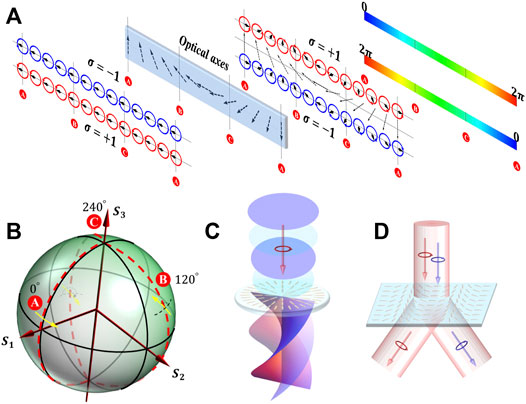
FIGURE 1. (A) Polarization evolutions under the modulation of artificial materials with spatially varying optical axes are constructed. The input and output SOPs are depicted in the first and third panels, respectively; red and blue circles represent the right- and left-circular polarizations, respectively; short arrows enclosed by these circles are the representations of instantaneous electric field vectors (corresponding to the phase shown in the fourth panel); dash arrow lines in the second panel show the orientations of local optical axes. It is shown that the circular polarization is reversed after passing through the material, and the orientation of the instantaneous electric field vectors is ordered by the orientation of local optical axes. (B) The Poincaré sphere are established to exhibit the evolution of SOP. Three evolving routes marked in red A, B, and C in the sphere highlight the evolutions under the optical axes with orientation angles
To precisely calculate the phase changes, a Poincaré sphere is applied to concretize the polarization space, which is a unit sphere involving all the homogenous polarization states, as shown in Figure 1B. Normalized Stokes parameters (
The evolutions can be retrieved mathematically by the Jones calculus, which is a universal tool to analyze light propagation in different materials. The Jones matrix for a homogenous wave plate with a fixed optical axis (
where
where
where
where
As the additional phase is related to the orientation of local optical axes, elements requiring complex phase modulation can be achieved without increasing the processing precision by using the PB phase. Theoretically, cascading of optical phase gradient devices equals the superposition of phases provided by each single element. Thus, the integration of a finite number of phase gradient elements can be achieved by constructing a device with the superposed phase profile. As the periodicity of the phase value, the superposed phase profile can be reduced to the interval
Figure 2 shows a simple example to explain our principle. The vortex beam generator (Figure 1A) and circular polarization splitter (Figure 1B) are integrated to get a polarization (spin)-dependent vortex beam splitter (Figure 1C). Figure 2A shows the phase profile
which is shown in Figure 2C. A representative point (
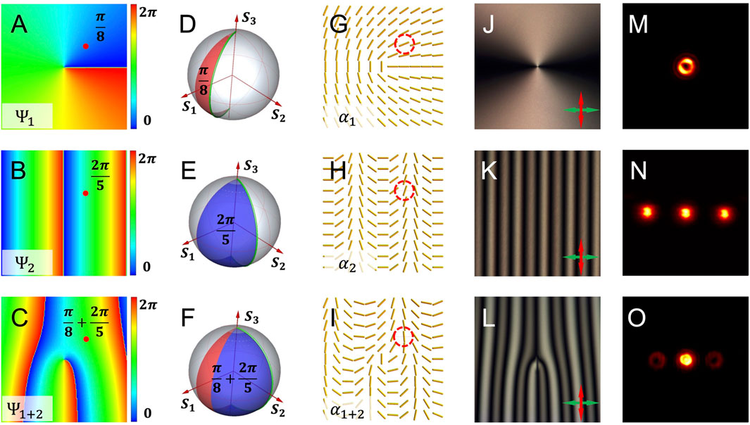
FIGURE 2. Design process of a vortex beam splitter is decomposed to demonstrate the principle of PB phase integration. (A–C) Superposition of a vortex phase (A) and a linear gradient phase (B) shows a fork-shaped phase (C). A selected point is highlighted with a red dot to show the superposition of phase values. (D–F) Poincaré spheres demonstrate the polarization evolving routes (green longitude lines) for the desired phase changes (colored regions) corresponding to the specific point in (A–C), respectively. It is shown that the phase changes can be achieved by controlling the evolving routes. (G–I) Desired distributions of the optical axes are painted, which correspond to the devices with phase profiles exhibited in the first column. (J–L) Polariscopic analyses are applied to verify the distributions of local optical axes. Red and green arrows represent the orientation of incident polarization and the analyzer, respectively. (M–O) Experimental intensities obtain by testing the corresponding devices.
Figures 2G–I are the expected optical axis distributions of the corresponding phase profiles.
To verify our designs, the femtosecond laser writing technique is applied to obtain the dielectric planar samples operating in a wavelength of
To show the ability of our principles for designing complicated planar devices, several compact PB phase devices are constructed as follows. First, we constructed a convertor for the LG and HG modes. Both modes are the acceptable forms of transverse distributions of the electric field in laser cavities [24], enabling unique practical applications in particle manipulation [25, 26], light communication [27], and laser processing [28]. The LG mode can be decomposed into a set of HG modes with the same order, and vice versa [29]. In traditional optics, a pair of cylindrical lenses can realize the conversion between LG and HG modes [30]. However, this kind of convertor cannot be miniaturized as suitable separation between the lenses should be maintained to achieve the transform.
Both LG and HG modes are widely used in laser applications. However, the conversion between them does not seem straightforward because different sources are always needed to produce these two modes in practical experiments. Most recently, a PB phase device for the conversion between the general Gaussian mode and the HG mode has been proposed [31]. Thus, in the optical integration way, the convertor for the LG and HG modes can be achieved by cascading two independent devices: an LG-to-Gaussian mode converter and a Gaussian-to-HG mode converter. The example of phase profiles of these two devices is demonstrated in Figure 3A (for HG11) and Figure 3B (for LG01). Following the designing principles introduced previously, the superposed phase profile and corresponding optical axis distribution are presented in Figures 3C,D. Figure 3E,F show the polariscopic analysis results under parallel and perpendicular linear polarizers, respectively. Then, the convertor is examined by an HG11 (Figure 3G) beam and an LG01 (Figure 3J) beam. Intensities shown in Figures 3H,K present the results of obtained LG01 and HG11 modes, respectively. To further verify the results, interference experiments with a general Gaussian beam are implemented. A typical fork-shaped dislocation shown in Figure 3I confirms the existence of the LG01 mode. The mismatches of fringe arrays in Figures 3L,M represent the phase mutation in the direction orthogonal to the fringes in the tested field, which verifies that the converted field is an HG11 mode.
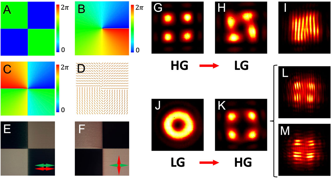
FIGURE 3. (A–C) Phase profiles of the HG11 mode, LG01 mode, and integrated phase. (D) Distribution of local optical axes of the desired mode converter. (E,F) Polariscopic analysis results of the constructed device. Red and green arrows indicate the orientations of the incident polarization state and the orientation of the analyzer. (G–I) Experimental intensities obtained when the device is working as an HG-to-LG mode converter. The incident HG11 mode (G) and obtained LG01 mode (H) are demonstrated. Interference fringes (I) imply the phase singularity in the obtained LG01 mode. (J–M) Experimental intensities obtained when the device is working as an LG-to-HG mode converter. (J,K) are the intensity patterns of the incident and obtained beams. (L,M) Phase mutations in horizontal and vertical directions, respectively.
Second, we build a higher order Bessel–Gaussian (BG) beam generator. OAM provides an infinite volume for data coding and shows a new degree of freedom in light manipulation, which is substantially determined by the spatial property of the beam [21]. Vortex beam possessing winding phase distribution around its central axis is inherently endowed with a non-zero OAM [32]. Generally, the PB phase arises from the spin (polarization)–orbit interactions in light, thus presenting good ability in controlling these two degrees of freedom. In particular, the PB phase is widely applied in the design of vortex devices in planar optics. BG beams provide an alternative solution for OAM-carrying beams [33]. A zero-order BG beam possess a bright central spot, while higher order BG beams show a dark center as the presentation of phase singularity. Similar to the higher order LG mode, the higher order BG beams possess a vortex phase term
The phase profile of a typical zero-order BG mode is a set of equal-width concentric annuluses, where the adjacent annuluses are endowed with distinct phase values in a difference
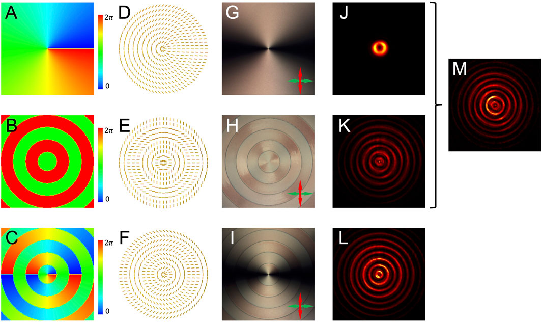
FIGURE 4. (A–C) Phase profiles of vortex, zero-order BG, and first-order BG beams. (D–F) Local optical axis distributions of expected PB phase devices corresponding to the phase profiles in the first column. (G–I) Polariscopic analysis results. (J–L) Experimental intensities obtained by using the samples corresponding to (G–I). (M) Intensity recorded when the vortex (G) and zero-order BG (H) generators are cascaded to get the first-order BG.
The last example is an attempt to construct a compact SAM-OAM splitter. The SAM and OAM multiplexing techniques promise to enlarge the capacity of light communications in the fiber and free space. However, the splitting of different OAM modes is still complicated. A general way is to use the phase plates with particular profiles to split the modes one by one [24], which is too complicated to integrate in planar optical devices. Fork-shaped phase devices (similar to our example shown in Figure 2) have been proposed to divide the different OAM modes simultaneously [38]. However, these devices are restricted to split the opposite OAM modes in the same order. In particular, when SAM is considered in the system, the splitting system will become more and more complicated with the increasing of SAM and OAM channels.
Here, we show the solution by using a compact planar dielectric device. Figure 5 is the compact SAM and OAM splitter. As mentioned before, the linear gradient PB phase device (Figure 1D) can be used to separate different SAM states. However, in this case, the different SAM states are deflected to opposite directions. To solve this problem, we divide the phase plane to different annuluses, the phase gradients in different districts are varied and the signs of the gradients are opposite in the adjacent districts. To involve the different OAM states, each district is assigned with a vortex phase with different topological charges. Thus, the constructed phase is shown in Figure 5A, where the phase plane is divided in two districts for OAM states
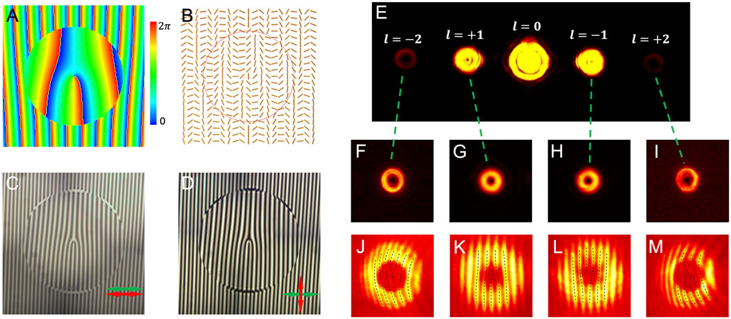
FIGURE 5. (A) Phase profile with two distinct parts along its radial direction. The inner part is designed with OAM
The fabricated samples were constructed inside a silicon dioxide glass substrate. A polarized high-power femtosecond laser source was focused to a point under the surface of the substrate to induce the sub-wavelength grating. The process could be understood in an interference mechanism. A plasma electron wave would present in the glass after absorbing the energy of the photons of the writing beam. Components of the plasma electron wave in the plane of incident polarization would interfere with the writing beam. Thus, the negative electrons included in the illuminated area were redistributed, which led to the rearrangement of ionized oxide atoms. The structure was “frozen” after reaching the hot equilibrium, and finally, a grating in size comparable with the wavelength of writing laser was exhibited. The grating structure led to the birefringence of light in a specific wavelength. The effective ordinary and extraordinary refractive indexes could be obtained after a linear approximation:
where
The polariscopic analyses were implemented under a polarized light microscope. The incident and detect polarizations were both adjusted by a flat polarizer. A digital camera recorded the pictures behind the eyepiece lens, and the magnification time was
We have developed a convenient way to construct compact planar PB phase devices by integrating the phase profiles of separated elements. The superposition of PB phases is theoretically analyzed through the Poincaré sphere method. Several proof-of-principle devices are constructed by using the high-transmission efficiency dielectric sub-wavelength structures. The intensity distributions modulated by the conceived devices show a good agreement with expectations. It is worth noting that our principles are not limited to realize a particular planar device, which provides an intuitive way to construct novel PB phase elements and demonstrates a way to circumvent the higher transmission loss in a complex optical system. It can be applied to simplify all the cascaded phase-controlling elements in optical circuits. Our reported general principles extend the way to realize complicated planar devices, ushering in the area of light manipulation and communications.
The original contributions presented in the study are included in the article/Supplementary Material, further inquiries can be directed to the corresponding author.
All authors listed have made a substantial, direct, and intellectual contribution to the work and approved it for publication.
This work is supported by the National Natural Science Foundation of China (Grant Nos. 11904238, 11734012, and 12074267).
The authors declare that the research was conducted in the absence of any commercial or financial relationships that could be construed as a potential conflict of interest.
All claims expressed in this article are solely those of the authors and do not necessarily represent those of their affiliated organizations, or those of the publisher, the editors, and the reviewers. Any product that may be evaluated in this article, or claim that may be made by its manufacturer, is not guaranteed or endorsed by the publisher.
1. Chow E, Lin SY, Johnson SG, Villeneuve PR, Joannopoulos JD, Wendt JR, et al. Three-dimensional Control of Light in a Two-Dimensional Photonic crystal Slab. Nature (2000) 407:983–6. doi:10.1038/35039583
2. Hikmet RAM, Kemperman H. Electrically Switchable Mirrors and Optical Components Made from Liquid-crystal Gels. Nature (1998) 392:476–9. doi:10.1038/33110
3. Yu N, Capasso F. Flat Optics with Designer Metasurfaces. Nat Mater (2014) 13:139–50. doi:10.1038/nmat3839
4. Meinzer N, Barnes WL, Hooper IR. Plasmonic Meta-Atoms and Metasurfaces. Nat Photon (2014) 8:889–98. doi:10.1038/nphoton.2014.247
5. Kildishev AV, Boltasseva A, Shalaev VM. Planar Photonics with Metasurfaces. Science (2013) 339:1232009. doi:10.1126/science.1232009
6. Huang L, Chen X, Mühlenbernd H, Zhang H, Chen S, Bai B, et al. Three-dimensional Optical Holography Using a Plasmonic Metasurface. Nat Commun (2013) 4:2808. doi:10.1038/ncomms3808
7. Aieta F, Genevet P, Kats MA, Yu N, Blanchard R, Gaburro Z, et al. Aberration-free Ultrathin Flat Lenses and Axicons at Telecom Wavelengths Based on Plasmonic Metasurfaces. Nano Lett (2012) 12:4932–6. doi:10.1021/nl302516v
8. Zheludev NI, Kivshar YS. From Metamaterials to Metadevices. Nat Mater (2012) 11:917–24. doi:10.1038/nmat3431
9. Li L, Jun Cui T, Ji W, Liu S, Ding J, Wan X, et al. Electromagnetic Reprogrammable Coding-Metasurface Holograms. Nat Commun (2017) 8:197. doi:10.1038/s41467-017-00164-9
10. Berry MV. The Adiabatic Phase and Pancharatnam's Phase for Polarized Light. J Mod Opt (1987) 34:1401–7. doi:10.1080/09500348714551321
11. Bomzon Ze., Biener G, Kleiner V, Hasman E. Space-variant Pancharatnam-Berry Phase Optical Elements with Computer-Generated Subwavelength Gratings. Opt Lett (2002) 27:1141–3. doi:10.1364/OL.27.001141
12. Maguid E, Yulevich I, Veksler D, Kleiner V, Brongersma ML, Hasman E. Photonic Spin-Controlled Multifunctional Shared-Aperture Antenna Array. Science (2016) 352:1202–6. doi:10.1126/science.aaf3417
13. Hasman E, Kleiner V, Biener G, Niv A. Polarization Dependent Focusing Lens by Use of Quantized Pancharatnam-Berry Phase Diffractive Optics. Appl Phys Lett (2003) 82:328–30. doi:10.1063/1.1539300
14. Chen X, Huang L, Mühlenbernd H, Li G, Bai B, Tan Q, et al. Dual-polarity Plasmonic Metalens for Visible Light. Nat Commun (2012) 3:1198. doi:10.1038/ncomms2207
15. Beresna M, Gecevičius M, Kazansky PG, Gertus T. Radially Polarized Optical Vortex Converter Created by Femtosecond Laser Nanostructuring of Glass. Appl Phys Lett (2011) 98:201101. doi:10.1063/1.3590716
16. Liu Y, Ling X, Yi X, Zhou X, Luo H, Wen S. Realization of Polarization Evolution on Higher-Order Poincaré Sphere with Metasurface. Appl Phys Lett (2014) 104:191110. doi:10.1063/1.4878409
17. Li S, Li X, Zhang L, Wang G, Zhang L, Liu M, et al. Efficient Optical Angular Momentum Manipulation for Compact Multiplexing and Demultiplexing Using a Dielectric Metasurface. Adv Opt Mater. (2020) 8:1901666. doi:10.1002/adom.201901666
18. Jin Z, Janoschka D, Deng J, Ge L, Dreher P, Frank B, et al. Phyllotaxis-inspired Nanosieves with Multiplexed Orbital Angular Momentum. eLight (2021) 1:1–11. doi:10.1186/s43593-021-00005-9
19. Ding X, Monticone F, Zhang K, Zhang L, Gao D, Burokur SN, et al. Ultrathin Pancharatnam-Berry Metasurface with Maximal Cross-Polarization Efficiency. Adv Mater (2015) 27:1195–200. doi:10.1002/adma.201405047
20. Ling X, Zhou X, Yi X, Shu W, Liu Y, Chen S, et al. Giant Photonic Spin Hall Effect in Momentum Space in a Structured Metamaterial with Spatially Varying Birefringence. Light Sci Appl (2015) 4–e290. doi:10.1038/lsa.2015.63
21. Zheng G, Mühlenbernd H, Kenney M, Li G, Zentgraf T, Zhang S. Metasurface Holograms Reaching 80% Efficiency. Nat Nanotechnol (2015) 10:308–12. doi:10.1038/nnano.2015.2
22. Lin D, Fan P, Hasman E, Brongersma ML. Dielectric Gradient Metasurface Optical Elements. Science (2014) 345:298–302. doi:10.1126/science.1253213
23. Yi X, Ling X, Zhang Z, Li Y, Zhou X, Liu Y, et al. Generation of Cylindrical Vector Vortex Beams by Two Cascaded Metasurfaces. Opt Express (2014) 22:17207–15. doi:10.1364/OE.22.017207
24. Allen L, Padgett MJ, Babiker M. IV the Orbital Angular Momentum of Light. Prog Opt (1999) 39:291–372. doi:10.1016/S0079-6638(08)70391-3
25. Padgett M, Bowman R. Tweezers with a Twist. Nat Photon (2011) 5:343–8. doi:10.1038/nphoton.2011.81
26. Paterson L, MacDonald MP, Arlt J, Sibbett W, Bryant PE, Dholakia K. Controlled Rotation of Optically Trapped Microscopic Particles. Science (2001) 292:912–4. doi:10.1126/science.1058591
27. Wang J, Yang J-Y, Fazal IM, Ahmed N, Yan Y, Huang H, et al. Terabit Free-Space Data Transmission Employing Orbital Angular Momentum Multiplexing. Nat Photon (2012) 6:488–96. doi:10.1038/nphoton.2012.138
28. Toyoda K, Miyamoto K, Aoki N, Morita R, Omatsu T. Using Optical Vortex to Control the Chirality of Twisted Metal Nanostructures. Nano Lett (2012) 12:3645–9. doi:10.1021/nl301347j
29. Beijersbergen MW, Allen L, Van der Veen HELO, Woerdman JP. Astigmatic Laser Mode Converters and Transfer of Orbital Angular Momentum. Opt Commun (1993) 96:123–32. doi:10.1016/0030-4018(93)90535-D
30. Allen L, Beijersbergen MW, Spreeuw RJC, Woerdman JP. Orbital Angular Momentum of Light and the Transformation of Laguerre-Gaussian Laser Modes. Phys Rev A (1992) 45:8185–9. doi:10.1103/PhysRevA.45.8185
31. He Y, Liu Z, Liu Y, Zhou J, Ke Y, Luo H, et al. Higher-order Laser Mode Converters with Dielectric Metasurfaces. Opt Lett (2015) 40:5506–9. doi:10.1364/OL.40.005506
32. Bliokh KY, Rodríguez-Fortuño FJ, Nori F, Zayats AV. Spin-orbit Interactions of Light. Nat Photon (2015) 9:796–808. doi:10.1038/nphoton.2015.201
33. McGloin D, Dholakia K. Bessel Beams: Diffraction in a New Light. Contemp Phys (2005) 46:15–28. doi:10.1080/0010751042000275259
34. Planchon TA, Gao L, Milkie DE, Davidson MW, Galbraith JA, Galbraith CG, et al. Rapid Three-Dimensional Isotropic Imaging of Living Cells Using Bessel Beam Plane Illumination. Nat Methods (2011) 8:417–23. doi:10.1038/nmeth.1586
35. Fahrbach FO, Gurchenkov V, Alessandri K, Nassoy P, Rohrbach A. Self-reconstructing Sectioned Bessel Beams Offer Submicron Optical Sectioning for Large fields of View in Light-Sheet Microscopy. Opt Express (2013) 21:11425–40. doi:10.1364/OE.21.011425
36. Garcés-Chávez V, McGloin D, Melville H, Sibbett W, Dholakia K. Simultaneous Micromanipulation in Multiple Planes Using a Self-Reconstructing Light Beam. Nature (2002) 419:145–7. doi:10.1038/nature01007
37. McLaren M, Mhlanga T, Padgett MJ, Roux FS, Forbes A. Self-healing of Quantum Entanglement after an Obstruction. Nat Commun (2014) 5:3248. doi:10.1038/ncomms4248
Keywords: planar optics, dielectric devices, Pancharatnam–Berry, optical integration, orbital angular momentum, artificial material
Citation: Liu Y and Wang GP (2022) Beam Manipulations With Compact Planar Dielectric Pancharatnam–Berry Phase Devices. Front. Phys. 10:894703. doi: 10.3389/fphy.2022.894703
Received: 12 March 2022; Accepted: 04 April 2022;
Published: 02 May 2022.
Edited by:
Hailu Luo, Hunan University, ChinaReviewed by:
Lei Zhang, Xi’an Jiaotong University, ChinaCopyright © 2022 Liu and Wang. This is an open-access article distributed under the terms of the Creative Commons Attribution License (CC BY). The use, distribution or reproduction in other forums is permitted, provided the original author(s) and the copyright owner(s) are credited and that the original publication in this journal is cited, in accordance with accepted academic practice. No use, distribution or reproduction is permitted which does not comply with these terms.
*Correspondence: Guo Ping Wang, Z3B3YW5nQHN6dS5lZHUuY24=
Disclaimer: All claims expressed in this article are solely those of the authors and do not necessarily represent those of their affiliated organizations, or those of the publisher, the editors and the reviewers. Any product that may be evaluated in this article or claim that may be made by its manufacturer is not guaranteed or endorsed by the publisher.
Research integrity at Frontiers
Learn more about the work of our research integrity team to safeguard the quality of each article we publish.