 Yuhan Liu1
 Dongfeng Qi
 Hongyu Zheng
94% of researchers rate our articles as excellent or good
Learn more about the work of our research integrity team to safeguard the quality of each article we publish.
Find out more
ORIGINAL RESEARCH article
Front. Phys., 10 March 2022
Sec. Optics and Photonics
Volume 10 - 2022 | https://doi.org/10.3389/fphy.2022.845576
This article is part of the Research TopicAdvances in Laser Micro-Processing and ApplicationsView all 5 articles
In this research, the pump-probe imaging technology and the time-resolved transmittance measurements are used to investigate the transient time scale of the oxidation area, the dewetted melt pool, and the ablation-induced mass transport, and their dependence on the incident laser. Moreover, the evolution time of various morphologies have been studied through a certain delay time from 10 to 30 ns with different dynamic processes. Meanwhile, the underlying formation mechanism and the phase change pathway have been studied. In this regard, a nanosecond (ns) pulsed laser with 532 nm wavelength was used to fabricate nanostructures on the surface of the thin Copper (Cu) films. The observations confirmed that the oxidation process of Cu plays a significant role in the mechanism of laser fluence-dependent oxidation, melting, and ablation dynamics. The results revealed that the different characteristics of the Cu film are related to the incident laser pulse energy. Furthermore, the experimental evidence was in good agreement with the SEM images and the Raman spectra. It is found that the Cu2O surface-rim with a central hole could be fabricated with the laser fluences above the ablation threshold. Although, for the laser fluences below the ablation threshold, the Cu2O phase can be formed in the central region.
Nowadays, nanostructures are considerably employed in various applications such as microelectronics, optoelectronics, biology, and sensing [1]. The vast applications of nanostructures have attracted great attention to design and fabricate nanostructures with lower costs and better geometrical and morphological characteristics. In this regard, several methods have been developed to fabricate surface-supported nanostructures [2, 3]. Among these methods, laser-induced nanostructure has the advantages of generating micrometer to nanometer structures, low thermal damage, non-contact nature, flexibility, non-planar fabrication [4–6]. Moreover, the possibility of creating a broad range of nanostructure by simply selecting the laser parameters (such as energy density, pulse duration, wavelength, and the number of pulses) gives laser-induced nanostructure a distinct advantage over other methods [7].
In this process, the laser irradiates to the surface of the substrate and causes deposition of the thin film on the surface of the substrate. Laser-induced nanostructure on the surface of the thin film includes several thermodynamic processes such as gasification, ablation, melting, and oxidation [8, 9]. Among different nanostructures categories, metal-based nanostructures have a great deal of research due to their unique optical, electronic, and sensing properties [10, 11]. For example, Copper (Cu), as an attractive metal for integrated circuits and flexible transparent conducting electrodes areas, is a fascinating alternative for producing nanostructures. It is worth mentioning that Cu is 90 times cheaper than silver (Ag) with similar electrical conductivity (Ag: 6.3 × 10⁷ S•m−1, Cu: 5.96 × 10⁷ S•m−1) [12]. Furthermore, the properties of Cu are significantly different from Ag, such as thermal conductivity (Ag: 428 W/mK, Cu: 401 W/mK) and heat capacity (Ag: 62.6 J/m3K2, Cu: 97 J/m3K2) [13, 14].
These processes can be controlled on the nanoscale to fabricate nanostructure with the desired geometrical and morphological characteristics [15]. Fundamental understanding of the phase change during oxidation, dewetting, and ablation processes of thin films is of great significance for improving the application of thin metal films in the manufacturing process of optoelectronics and microelectronic devices [16]. Therefore, it is necessary to understand the thermodynamic changes during laser-mater interaction. Until now, a number of optical detection methods have been employed to probe the transient dynamics of ablation. For instance, the shadowgraph imaging technique is primarily employed in characterizing mass ejection and plume generation. Moreover, the reflectance and the transmittance of thin films after pulsed laser irradiation are adequately captured by pump-probe technology [17].
Although the research on pulsed laser processing of thin films has been quite active and various research groups have carried out extensive research on the preparation of functional metal thin-film electrode materials, the precise transformation mechanism involving details has not been well understood. In particular, the induced time scale of phase changes during oxidation, dewetting, and ablation processes has not yet been thoroughly investigated. In this study, the imaging pump-probe technology and time-resolved transmittance measurements were combined to study the evolution of nanosecond (ns) laser-induced Cu film oxidation, dewetting, and ablation over time, paving the way for a better understanding of the nanosecond laser processing on Cu films.
The experimental setup is schematically shown in Figure 1, where Nd:YAG laser pulses with 532 nm wavelength and 20 ns pulse duration are irradiated on the Cu film. A 50 nm copper film was deposited on a 1 mm quartz substrate using a TRP-450 magnetron sputtering system. As it is not easy for Cu to deposit directly on a quartz substrate, the following steps were conducted for sample preparation. In the first step, 0.2–0.5 nm chromium (Cr) was plated on quartz substrate under the current of 0.1 A, room pressure of 0.6 Pa, and deposition time of 5 s. Subsequently, 50 nm Cu film was deposited under the current of 0.3 A, room pressure of 0.5 Pa, and deposition time of 200 s.
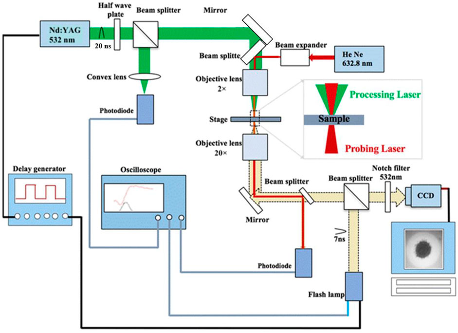
FIGURE 1. The schematic of the experimental setup including the laser system, the time-resolved imaging, and the pump-probing transmittance measurement setups.
For the time-resolved imaging system, the pump laser beam was focused by a 2× infinity-corrected and 60 mm working distance of objective lens at normal incidence. A nanosecond flash lamp (NANO LITE KL-K flash lamp, flash duration = 7 ns) was employed to provide temporally resolved illumination. Consequently, the images were captured by a charge-coupled-device (CCD) camera via a combination of a ×20 infinity objective lens and a 200 mm tube lens. A digital delay generator controlled the delay time between processing laser and image acquisition. For the transmission probing part, the same ns laser pulse was irradiated at normal incidence, and the 632.8 nm He-Ne continuous wave laser was incident perpendicularly to the center of the irradiated area. The Cu film sample was located on the focal plane of the detection laser. The specific position of the focal plane was determined by the knife-edge beam profile.
The beam diameters of the laser beam and detection beam were respectively measured 40 and 10 µm by the knife-edge method. The fluence of the transmittance probe signal was measured by a fast photodiode coupled to an oscilloscope. It should be noted that the temporal resolution of the time-resolved imaging experiment is limited by the duration of the flash lamp itself, and it is 7 ns in this case. The oscilloscope was used to record the actual delay time of the processing laser signal, the flash lamp signal, and the probing laser signal. At least four signals are checked in each delay setting to ensure the accuracy and credibility of the data.
The processing dynamics of the ns laser on the Cu film using the pump-probe technology and the time-resolved transmittance measurements are investigated in this study. According to the observations, three significant states, including oxidation, dewetting, and ablation, occur during Cu thin film laser structuring. As shown in Figure 2, the threshold of each state is related to the laser fluences. In detail, the optimal laser fluence can be obtained by the thermal properties of the substrate owing to the heat-transferred mechanism [18]. The oxidation, dewetting, and ablation thresholds of the Cu film are estimated by linear curve fitting, as shown in Figure 2. In order to establish the relationship between the laser energy density and the ablation hole diameter distribution, the ablation hole structures with different diameter distributions on the material surface were obtained by changing the laser energy density. The functional relationship between the incident laser energy density and the ablation hole radius is as follows [19]:
Where,
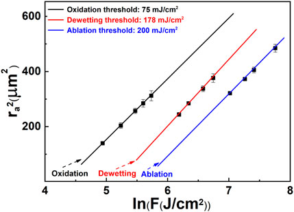
FIGURE 2. Normalized laser intensities of the oxidation, dewetting and ablation threshold on the Cu thin film.
It is depicted that after the direct laser writing, the surface of the material can be heated and melted rapidly and can reach an overheated state that exceeds the boiling point. At this time, the material vapor pressure will be greater than the ambient pressure [20]. On the one hand, the vapor pressure in the gas phase forces the metal vapors to separate from the matrix. On the other hand, it pushes the metal to melt. When the gasification back pressure of the metal melt exceeds the reverse restraining force, such as the surface tension of the melt, the ablated part of the Cu film is ejected, and the unablated part is still attached to the substrate. The dewetting holes emerge after the laser fluence (red curve, Figure 2) reached the dewetting threshold (178 mJ/cm2). The formation of holes is the effect of surface energy minimization once the Cu film experienced partial melting. The location is determined by the heterogeneous nucleation. Furthermore, a continuous network of dewetting holes appears with higher fluence (Figure 3A). At the center of the network, some dewetted islands are formed by the complete melting-induced localized dewetting. If the laser fluence exceeds the ablation threshold (200 mJ/cm2), ablation starts happening in the center of the processed area, and dewetting region is expanding towards further outside (Figure 3A).
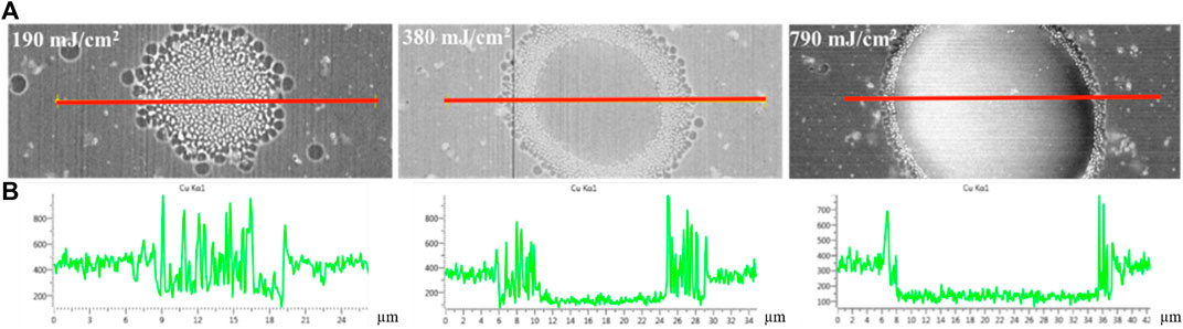
FIGURE 3. (A) SEM-line EDS images of structures produced using laser fluence of 190 mJ/cm2, 380 mJ/cm2, and 790 mJ/cm2, respectively. (B) Selected time-resolved images with 60 ns delayed under different laser intensities.
The surface morphology and the element distribution of Cu film at different energy fluences are examined by the SEM images (Figure 3). Moreover, the surface element distribution graphs and time-resolved images of the 50 nm Cu film surface after irradiation with different laser energy fluences are shown in Figure 3. It has been demonstrated that when the incident laser energy fluence is lower than 200 mJ/cm2, droplet-like structures will be formed in the central region, while the Cu element is much higher, which means that the central point has melted and dewetted. With the increase of fluence (380 mJ/cm2), the central droplet structure is replaced by the ablated hole structure, and the melted material is dehumidified radially outward. At a higher laser energy fluence (790 mJ/cm2), the diameter of the ablated hole becomes larger, and the particle area in the edge molten state becomes narrower. It is worth noting that there are some peripheral rims and droplet fingers at the edge of the spot where the Cu element is much higher. It is found that the surface temperature is higher at the center of the melt pool, and the absorbed energy induces surface tension-driven flow due to the high-temperature gradient. Consequently, due to the diminishing surface tension with increasing temperature for liquid metals, the material should be transported radially outward by the positive surface tension gradient [21, 22].
Micro-Raman spectroscopy is employed for the material characterization of the Cu oxidation, dewetting, and ablation spot. Figure 4 shows the Raman spectra of different areas (center, inner edge, and outer edge) of the material surface at different laser fluences. Besides, the time-resolved optical images and the SEM images corresponding to the Raman spectra are also displayed to evaluate the morphological changes and the optical properties. The Raman spectrum of the Cu oxide in the air is presented in Figure 4A. Two peaks at the 516 and 615 cm−1 are characteristic of the Cu2O phase. This phase appears at the center spot areas. The existence of Cu2O is in agreement with previous researches [23, 24]. By increasing the laser fluence to190 mJ/cm2, two peaks located at the 516 and 615 cm−1 are characteristic of the Cu2O phase appear in the center spot (Figure 4B). The corresponding SEM image [Figure 4(b2)] indicates the dewetting induced droplet-like structure is the Cu2O phase. Besides, if the laser fluence is above the ablation threshold (as shown in Figure 4C), two peaks located at the 516 and 615 cm−1 are characteristic of the Cu2O phase appear at the inner and outer rim areas. The existence of Cu2O agrees with previous researches [23–26]. Ablation happens in the center region of the spot; therefore, no peaks are expected. The further comparison reveals that the intensities of these two peaks in the inner-rim region are higher than that of the dewetting and oxidation area. Since the inner rim receives a higher laser energy input, undergoes complete melting and dewetting, the elevated temperature and liquid state facilitate the oxidation process, which leads to stronger Cu2O formation. The different nanostructures may be related to the dewetting process, and the growth region changes significantly, resulting in the formation of unique nanostructures in the same range. Sputtering-deposited flims containing a lot of atomic vacancies and defects. When sufficient thermal energy is supplied, the adatoms can begin to diffuse and induce the nucleation of pinholes from the vacancies in the as-depositedfilm. Along with the dewetting process, the pinholes will develop to be larger. At the same time, the coalescence growth model indicates that the lateral growth and merging between nanostructures can occur along with the increased deposition amount [27]. As a contrast group, the Raman spectrum of Cu thin films after laser irradiation in the N2 gas protection is also investigated, and there is no Cu2O phase appears after laser irradiation, which means Cu film is stable in the N2 gas protection, as shown in Figure 4D. Cu film can also be oxidized even under ns pulse laser irradiation, and N2 atmosphere will be required for improving electrical performance further.
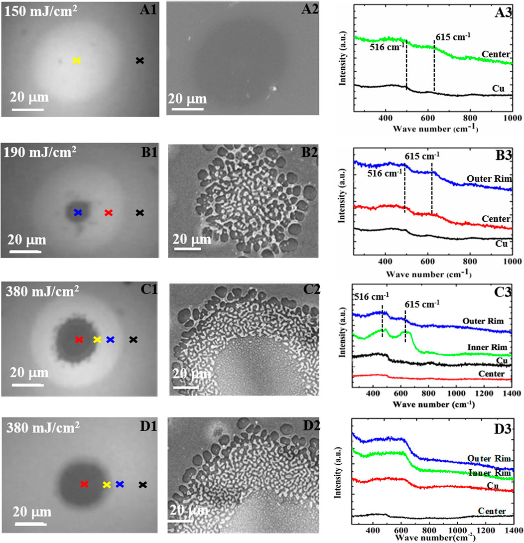
FIGURE 4. Time-resolved optical images (a1-d1) and SEM images (a2-d2) with corresponding Raman spectra (a3-d3) for edge, rim, and center regions of dot structures shown on the right, (A) irradiated Cu at 150 mJ/cm2, (B) irradiated Cu at 190 mJ/cm2, (C) irradiated Cu at 380 mJ/cm2, (D) irradiated Cu at 380 mJ/cm2 by the N2 gas protection. The scale bars in the time-resolved optical images and SEM images are all 20 μm.
Figure 5A shows a schematic diagram of the ablation, dewetting, and oxidation distribution on the surface of the Cu film under different laser fluences. As it can be seen in this figure, if the laser fluence is higher than the ablation threshold (blue curve), there will be three areas on the surface of the material: the ablation hole area in the center of the spot, the Cu2O granular area around the hole, and the Cu2O film structure around the spot. If the laser fluence is between the dewetting threshold and the ablation threshold (red curve), the Cu2O granular region will appear in the center of the spot, and the Cu2O thin film structure will still appear in the peripheral area of the spot. When the laser fluence is lower than the dewetting threshold and higher than the oxidation threshold (black curve), only the oxide layer structure in the form of Cu2O will appear in the central area of the spot.
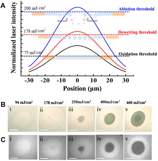
FIGURE 5. Energy-dependent oxidation, dewetting, and ablation states. (A) Normalized laser intensities of the oxidation, dewetting, and ablation threshold on the Cu thin film with corresponding introduced oxidation, dewetting, and ablation sizes. Absorbed laser intensities are normalized by the peak intensities of the blue curve. (B) Ex-situ optical bright-field microscopy images of the processed morphology with different laser fluences. (C) In-situ time-resolved reflection images of morphologies with corresponding fluences captured at 40 ns after irradiation (The scale bars are 20 μm).
The transient dynamics of laser interaction with Cu film are revealed by the time-resolved imaging and transmission probing. Figure 6 shows the evolution of the surface morphology and the transmittance of the Cu film at different laser energy fluences over time. The normal transmittance traces were normalized with respect to their initial values before laser irradiation. From Figure 6(a1), it is noticed that under low laser fluence irradiation (150 mJ/cm2, 178 mJ/cm2), the transmittance directly drops to a lower state (<2). In this case, the decrease of transmittance can be attributed to the effect of oxidation since the oxidation gives a brighter field in the optical image (Figure 2), indicating a stronger reflection. For a laser fluence of about 190 mJ/cm2, micron-sized droplet particles will be formed in the center of the spot. It can be found from Figure 6(a2) that a shining particle structure can be formed in the central area of the spot within 13 ns after laser irradiation, which may be the result of Ostwald ripening [3].
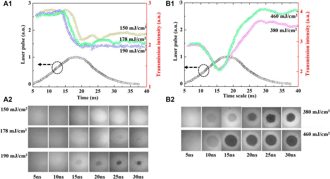
FIGURE 6. The transmission probing curve and their corresponding time-resolved image series of ns laser-induced dewetting and oxidation process with different laser fluences: (a1, a2) 150 mJ/cm2, 178 mJ/cm2, 190 mJ/cm2, (b1, b2) 380 mJ/cm2, 460 mJ/cm2 (Each frame is taken at a certain flash lamp delay time).
Furthermore, it can be seen that after 20 ns, the central region in the reflected image is dark. The reason for this is that the micron-sized metal particles (
Based on our fundamental work on the laser-matt, the transmittance measurement validated the dynamics of oxidation, dewetting, and ablation process. Besides, the evolution process and evolution time of various morphological features on the surface of Cu thin films under specific laser fluences at a certain delay time are accurately recorded by combining the time-resolved imaging techniques [28].
In summary, we have systematically studied the interaction between the laser beam and the Cu thin films and demonstrated the changes of morphological and thermodynamic properties of the Cu thin films during the interaction between the ns laser and the Cu thin films at specific time scales. In this regard, three main states during laser structuring of Cu films, i.e., oxidation, dewetting, and ablation, were investigated by time-resolved imaging and pump-probing technology. The observations indicate that after the ns laser irradiation, copper is directly oxidized to the Cu2O in the center, inner rim, or outer rim with different laser fluences. The time decay of the oxidation and dewetting process for Cu was obtained approximately from 15 to 13 ns, respectively. While it is noticed that under high fluence (above ablation threshold), the transmittance first drops (10 ns) and then increases stabilize at a higher transmission state (15 ns), and the timescale of the whole process needs about 28 ns In this case, it is possible to make a more explicit explanation and description of the starting time and the timescale of the whole processing. They are found to be in good agreement with the time-resolved image results. Therefore, the results pave the road towards a further understanding of the scale distribution of the total duration of laser-Cu film interaction.
The original contributions presented in the study are included in the article/supplementary material, further inquiries can be directed to the corresponding author.
Among the authors in the list, YL designed the experiment; carried out nanofabrication, laser processing, and characterization; as well as analyzed the results. JZ contributed in carrying out experiment analysis. SS offered critical suggestions on the result summary of this work. TS helped perform the analysis with constructive discussions. HZ provided the necessary materials for the experiment. DQ is the corresponding author of this work.
This work was supported by Natural Science Foundation of Shandong (ZR2021MF030), Natural Science Foundation of Zhejiang (LY21F050002).
All claims expressed in this article are solely those of the authors and do not necessarily represent those of their affiliated organizations, or those of the publisher, the editors and the reviewers. Any product that may be evaluated in this article, or claim that may be made by its manufacturer, is not guaranteed or endorsed by the publisher.
The authors declare that the research was conducted in the absence of any commercial or financial relationships that could be construed as a potential conflict of interest.
The handling editor declared a past co-authorship with one of the authors DQ.
2. Veiko VP, Konov VI. Fundamentals of Laser-Assisted Micro-and Nanotechnologies. Springer (2014). p. 195.
3. Qi D, Paeng D, Yeo J, Kim E, Wang L, Chen S, et al. Time-resolved Analysis of Thickness-dependent Dewetting and Ablation of Silver Films upon Nanosecond Laser Irradiation. Appl Phys Lett (2016) 108:211602. doi:10.1063/1.4952597
4. Wang H, Qi D, Yu X, Zhang Y, Zhang X, Zhang Z, et al. Self-assemble SiGe Island Structures Formed by Nanosecond Laser Irradiation on SiGe Virtual Film. Optik (2018) 171:652–7. doi:10.1016/j.ijleo.2018.06.115
5. Naderi Bakhtiyari A, Wang Z, Zheng H. Feasibility of Artificial Neural Network on Modeling Laser-Induced Colors on Stainless Steel. J Manufacturing Process (2021) 65:471–7. doi:10.1016/j.jmapro.2021.03.044
6. Bakhtiyari AN, Wang Z, Wang L, Zheng H. A Review on Applications of Artificial Intelligence in Modeling and Optimization of Laser Beam Machining. Opt Laser Tech (2021) 135:106721. doi:10.1016/j.optlastec.2020.106721
8. Ionin AA, Klimachev YM, Kotkov AA, Kozlov AY, Seleznev LV, Sinitsyn DV. Carbon Monoxide Laser Emitting Nanosecond Pulses with 10MHz Repetition Rate. Opt Commun (2009) 282:294–9. doi:10.1016/j.optcom.2008.09.089
9. Ruffino F, Grimaldi MG. Nanostructuration of Thin Metal Films by Pulsed Laser Irradiations: A Review. Nanomaterials (2019) 9:1133. doi:10.3390/nano9081133
10. Fan Z, Huang X, Tan C, Zhang H. Thin Metal Nanostructures: Synthesis, Properties and Applications. Chem Sci (2015) 6:95–111. doi:10.1039/c4sc02571g
12. Paeng D, Yoo J-H, Yeo J, Lee D, Kim E, Ko SH, et al. Low-Cost Facile Fabrication of Flexible Transparent Copper Electrodes by Nanosecond Laser Ablation. Adv Mater (2015) 27:2762–7. doi:10.1002/adma.201500098
13. Liu D, Alexander DR. High Intensity Femtosecond Laser Pump‐probing Measurements of a Cu Surface. Appl Phys Lett (1995) 67:3726–8. doi:10.1063/1.115363
14. Aid SR, Matsumoto S, Fuse G. Boron Diffusion Behavior in Silicon during Shallow P +/n junction Formation by Non-melt Excimer Laser Annealing. Phys Status Solidi A (2011) 208:1646–51. doi:10.1002/pssa.201026531
15. Binns C. Introduction to Nanoscience and Nanotechnology: Tiny Structure, 1. John Wiley & Sons (2010).
16. David J, Hojeong J, Costas P, Jong Y, Richard E. Femto Second Laser Ablation Induced Plasma Characteristics from Submicron Craters in Thin Metal Film. Appl Phys Lett (2007) 91:251118.
17. Papazoglou DG, Karaiskou A, Zergioti I, Fotakis C. Shadowgraphic Imaging of the Sub-ps Laser-Induced Forward Transfer Process. Appl Phys Lett (2002) 81:1594–6. doi:10.1063/1.1497191
18. Furusawa K, Takahashi K, Kumagai H, Midorikawa K, Obara M. Ablation Characteristics of Au, Ag, and Cu Metals Using a Femtosecond Ti:sapphire Laser. Appl Phys A: Mater Sci Process (1999) 69:S359–S366. doi:10.1007/s003390051417
19. Jandeleit J, Urbasch G, Hoffmann HD, Treusch H-G, Kreutz EW. Picosecond Laser Ablation of Thin Copper Films. Appl Phys A (1996) 63:117–21. doi:10.1007/bf01567638
20. Ready JF. Effects Due to Absorption of Laser Radiation. J Appl Phys (1965) 36:462–8. doi:10.1063/1.1714012
21. Egry I, Ricci E, Novakovic R, Ozawa S. Surface Tension of Liquid Metals and Alloys - Recent Developments. Adv Colloid Interf Sci (2010) 159:198–212. doi:10.1016/j.cis.2010.06.009
22. Hergenröder R. Laser-generated Aerosols in Laser Ablation for Inductively Coupled Plasma Spectrometry. Spectrochim Acta, B (2006) 61:284–300.
23. Godbole M, Pedraza A, Lowndes D, Thompson J. Excimer Laser Irradiation of Metallic Films on Ceramic Substrates. MRS Online Proc Libr (1991) 235. doi:10.1557/proc-235-583
24. Wautelet M. Oxidation of Thin Cd, Cu and Te Films under Continuous Laser Irradiation. Mater Lett (1983) 2:20–2. doi:10.1016/0167-577x(83)90023-x
25. Chrzanowski J, Irwin JC. Raman Scattering from Cupric Oxide. Solid State Commun (1989) 70:11–4. doi:10.1016/0038-1098(89)90457-2
26. Goldstein HF, Kim D-s., Yu PY, Bourne LC, Chaminade J-P, Nganga L. Raman Study of CuO Single Crystals. Phys Rev B (1990) 41:7192–4. doi:10.1103/physrevb.41.7192
27. Sui M, Kunwar S, Pandey P, Zhang Q, Li M-Y, Lee J. Fabrication and Determination of Growth Regimes of Various Pd NPs Based on the Control of Deposition Amount and Temperature on C-Plane GaN. J Mater Res (2017) 32:3593–604. doi:10.1557/jmr.2017.272
Keywords: time-resolved image, pump- probe, nanosecond laser ablation, copper film, surface mophologies
Citation: Liu Y, Zhang J, Shangguan S, Qi D, Sun T and Zheng H (2022) Temporal-Spatial Measurement of Surface Morphological Evolution Time in Nanosecond Laser Irradiation on the Copper Film. Front. Phys. 10:845576. doi: 10.3389/fphy.2022.845576
Received: 30 December 2021; Accepted: 18 January 2022;
Published: 10 March 2022.
Edited by:
Andong Wang, CNRS, FranceReviewed by:
Yunxiang Pan, Nanjing University of Science and Technology, ChinaCopyright © 2022 Liu, Zhang, Shangguan, Qi, Sun and Zheng. This is an open-access article distributed under the terms of the Creative Commons Attribution License (CC BY). The use, distribution or reproduction in other forums is permitted, provided the original author(s) and the copyright owner(s) are credited and that the original publication in this journal is cited, in accordance with accepted academic practice. No use, distribution or reproduction is permitted which does not comply with these terms.
*Correspondence: Dongfeng Qi, cWlkb25nZmVuZ0BzZHV0LmVkdS5jbg==; Hongyu Zheng, emhlbmdob25neXVAc2R1dC5lZHUuY24=
Disclaimer: All claims expressed in this article are solely those of the authors and do not necessarily represent those of their affiliated organizations, or those of the publisher, the editors and the reviewers. Any product that may be evaluated in this article or claim that may be made by its manufacturer is not guaranteed or endorsed by the publisher.
Research integrity at Frontiers
Learn more about the work of our research integrity team to safeguard the quality of each article we publish.