- 1College of Integrated Circuit Science and Engineering, Nanjing University of Posts and Telecommunications, Nanjing, China
- 2Shanghai Aerospace Electronic Technology Institute, Shanghai, China
- 3School of Information Engineering, Nanchang Hangkong University, Nanchang, China
- 4Electrical and Electronic Laboratory Center, College of Electrical and Optical Engineering and College of Microelectronics, Nanjing University of Post and Telecommunications, Nanjing, China
- 5College of Electronic and Optical Engineering, College of Microelectronics, Nanjing University of Posts and Telecommunications, Nanjing, China
- 6National and Local Joint Engineering Laboratory of RF Integration and Micro-Assembly Technology, Nanjing, China
Conventional von Newmann-based computers face severe challenges in the processing and storage of the large quantities of data being generated in the current era of “big data.” One of the most promising solutions to this issue is the development of an artificial neural network (ANN) that can process and store data in a manner similar to that of the human brain. To extend the limits of Moore’s law, memristors, whose electrical and optical behaviors closely match the biological response of the human brain, have been implemented for ANNs in place of the traditional complementary metal-oxide-semiconductor (CMOS) components. Based on their different operation modes, we classify the memristor family into electronic, photonic, and optoelectronic memristors, and review their respective physical principles and state-of-the-art technologies. Subsequently, we discuss the design strategies, performance superiorities, and technical drawbacks of various memristors in relation to ANN applications, as well as the updated versions of ANN, such as deep neutral networks (DNNs) and spike neural networks (SNNs). This paper concludes by envisioning the potential approaches for overcoming the physical limitations of memristor-based neural networks and the outlook of memristor applications on emerging neural networks.
Introduction
Combining the age of 5G communication with the concept of the Internet of Everything (IoE) and the rise of the Internet of Things, data will be dispersed, stored, calculated, and analyzed to obtain the most efficient information. The most important aspect of technological evolution is the advancement of process levels and system-end design. However, the development of silicon CMOS-based computing hardware has largely limited progress, as Moore’s Law has become less applicable [1]. At the same time, the rapid increase of data volume has gradually revealed the limitations of computers based on the traditional Von Neumann architecture. Owing to the physical separation of storage and computation, traditional computers waste large amounts of energy but fail to achieve further improvements in computing power [2,3]. The development of edge computing, the Internet of Things, and artificial intelligence (AI), has led to an increased demand for systems with reduced power consumption, increased computing power, and algorithm versatility. In contrast to traditional computing systems, the information processing characteristics of the human brain and nervous system allow for large-scale parallel distributed storage and processing, self-organization, self-adaptation, and self-learning [4]. There is no clear boundary between data storage and processing in the human brain, which exhibits extraordinary advantages in dealing with unstructured data. In contrast, traditional computer architectures cannot detect targets or engage in emotional understanding. Compared to their biological counterparts, artificial sensing systems exhibit low classification accuracy, high power consumption, and low integration density. There is an urgent need for new computing models to re-empower human society’s ability to process big data. Options that have been examined include using a nonvolatile memory device, breaking the “storage wall,” simulating the human brain processing mechanism, and building integrated computing architectures that combine storage and computation hardware [5]. Hardware neural networks based on memristor synaptic devices has proven to be an important development for neuromorphic computing and a strong candidate to replace traditional von Neumann computing architecture in a post-Moorish era. The basic structure of a memristor is a sandwich-like multilayered stack of substances that include, in descending order, a top electrode, middle layers with several resistive functions, and a bottom electrode. Memristors have many ideal characteristics but a simple structure. Any two-terminal electrical device with a resistance switching property is a memristor [6,7]. For a bipolar memristor, application of a positive voltage can convert the device from a high-resistance state to a low-resistance state. This is called the SET process. Conversely, application of a negative voltage can convert the device from a low-resistance state to a high-resistance state, which is called the RESET process. As a result, the memristor – its device structure, material, and other aspects - was widely studied early on as an option for resistive switching memory and an optimized design scheme has been proposed. Examining the resistive switching mechanism of growth and the fracturing of the memristor’s conductive wire, Professor Lu Wei’s team at the University of Michigan verified in 2018 that the conductivity of a memristor can gradually change under voltage pulse excitation. That is, the conductive wire can gradually grow and break under external excitation [8]. The changes in voltage and current observed in the gradient conductance memristor are similar to the renewal of synaptic weight in the biological nervous system; thus, a memristor can simulate basic synaptic functions, including short-term plasticity (STP), long-term Potentiation (LTP), long-term depression (LTD), and spike time-dependent plasticity (STDP) [9–11]. Similar electrical characteristics make it possible for a memristor to fabricate neural networks that are more similar to biological nervous systems. Since this discovery, memristive synapse devices have become powerful candidates for new electronic synapse devices in neural morphology calculations. Given the outstanding properties of memristors, research and review of their use in the development of neural networks is particularly important to provide guidance for future engagement in corresponding applications and research. In this study, we discuss the categories of electronic, photonic, and optoelectronic memristors and summarize the materials used, the current state of memristor neural networks, and future prospective research areas.
Investigation of Memristor Storage Materials
Memristor are constructed of many materials that mainly consist of thin films, nanowires, and nanoparticles. Even insulating materials at the nanometer level are likely to have resistive characteristics. As shown in Figure 1, memristor storage media can be divided into two categories: organic and inorganic materials. Organic materials, mainly biomimetic organic materials (such as silk fibroin [12], protein [13], nanocellulose [14], and bovine serum albumin [15]), and polymer organic materials (such as PVPCz59 [16], PVDR [17], PVK-C60 [18], and other materials [19–25]), have attracted the attention of many researchers owing to their applications in flexible and wearable storage and disposable health diagnosis and monitoring equipment. However, the stability of organic materials leads to high SET/RESET voltage, high power consumption and dispersed SET/RESET voltage distribution, so the device performance needs to be further strengthened. In addition, the supply of materials is also an urgent problem to be solved [20–25]. Solid electrolyte, oxide, and low-dimensional inorganic memristive materials have attracted extensive attention from researchers owing to their simple manufacturing process, stable performance, and low cost. Current memristor research focuses on clarifying the resistive mechanism and stabilizing the resistive performance. Although the RS mechanism may be different because of variations in electrode and RS layer materials (such as oxygen vacancy accumulation or silver ion redox reaction) [26–29], researchers have proposed several solutions to improve memristor stability, including the addition of an interface layer, doping, the addition of nanocrystals, improving the preparation process, and improving the operation mode. The electrodes of these devices consist of mostly inert metals such as Pt, which can be replaced by TiN electrodes to eliminate etching difficulty in mass production. The long-term performance of these devices is promising. The following chapter focuses on inorganic memristive materials, including oxide materials, solid electrolyte materials, ferroelectric materials, and two dimensional (2D) materials.
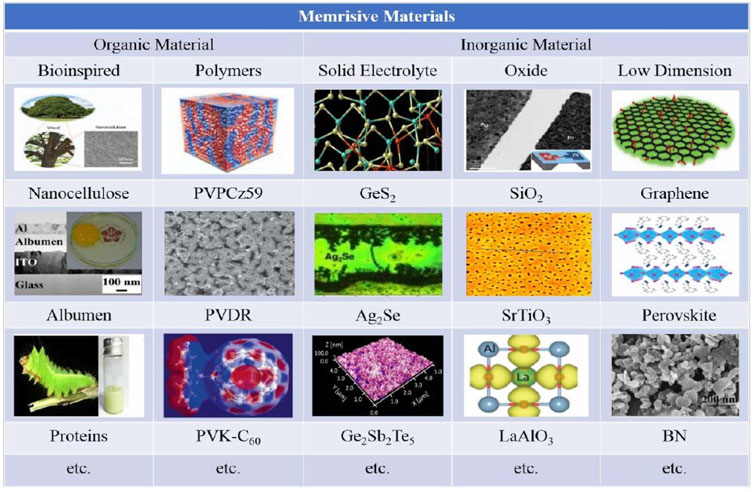
FIGURE 1. Memrisive material classification diagram [30].
Conventional Oxides
Owing to their simple fabrication process and compatibility with mature CMOS technology, binary oxides account for a large proportion of many types of electronic memristors. Figure 2 lists the elements that have been reported to have RS characteristics in binary oxides. The reported binary oxide materials used in RS layers such as silicon oxide (SiO2) [31], titanium oxide (TiO2) [32], vanadium oxide (VO2) [33], zirconium oxide (ZrO2) [34], nickel oxide (NiO) [35], zinc oxide (ZnO) [36], hafnium oxide (HfO2) [37], tantalum oxide (Ta2O5) [38], and alumina (Al2O3) [39] are WOx-based memristor materials [40] with good switching characteristics. Some exhibit low variability and low power operability. Moreover, by using different combinations of electrodes and dielectrics, memristors with mutation and gradient abilities can be realized, making them suitable for different simulation environments. For example, devices with a mutation ability are suitable for binary memory, and devices with a gradient ability are suitable for the multilevel storage of memory or for biological synaptic simulation.
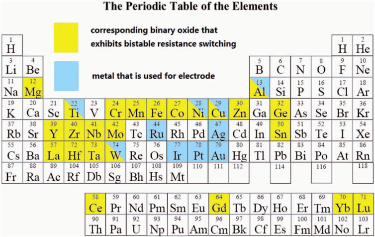
FIGURE 2. Summary of the materials that have been used for binary oxide memristor. Metals of the corresponding binary oxides used for the RS layer are in yellow. Metals used for the electrodes are in blue [41].
Since the HP team pioneered the solid memristor devices based on TiO2 materials in 2008 [42], several research groups have found memristive behaviors in different oxide materials. Owing to their simple fabrication process and compatibility with mature CMOS technology, binary oxides have become the mainstream materials of the electronic memristors. Figure 2 lists the common oxides that have been reported to have RS characteristics. The reported binary oxide materials used in RS layers mainly include silicon oxide (SiO2) [31], titanium oxide (TiO2) [32], vanadium oxide (VO2) [33], zirconium oxide (ZrO2) [34], nickel oxide (NiO) [35], zinc oxide (ZnO) [36], hafnium oxide (HfO2) [37], tantalum oxide (Ta2O5) [38], alumina (Al2O3) [39], and tungsten oxide (WOx) based materials [40], which exhibit good switching characteristics, low variability and low power operability. Moreover, by using different combinations of electrodes and dielectrics, memristors with mutation and gradient abilities can be realized, making them suitable for various applications from binary or multilevel storage memories to artificial synapses. In spite of vigorous developments on memristive materials, their memristive mechanisms still remain mysterious, which currently can be categorized into the conduction boundary migration mechanism, conduction filament regulation mechanism and Schottky barrier modulation mechanism.
The conduction boundary migration mechanism, first proposed by HP team, usually adapts to a tri-layer structure having an intermediate insulating layer sandwiched between top and bottom electrodes. As exemplified by a TiO2-based memristor (Figure 3A), its insulation layer consists of a thin undoped TiO2 film and a thin doped TiO2 film [42], which gives rise to low conductivity (ROFF) and high conductivity (RON), respectively, due to the increased oxygen vacancies. Such device was equivalent to a series of resistors with high and low resistance values. When an electric field is applied to the device, the oxygen vacancy migrates between the two layers, compressing the width of the undoped region and changing the device resistance. In addition to the double-layer memristor, monolayer oxide materials can also achieve memristive behavior. As shown in Figure 3B, when positive and negative voltage scanning is performed on the memristor [43] with Pd/WOx/W structure, the gradual reduction and increase of resistance confirm the memristor characteristics of the device. The regulation model of the number of conductive filaments provides the corresponding mechanism explanation: As shown in Figure 3C, the migration of oxygen ions under the action of applied voltage changes the number of oxygen vacancy conductive channels or the effective cross-sectional area. Due to the low resistance of oxygen vacancy conductive channels, the device resistance decreases when the number of oxygen vacancy conductive channels increases. As the number decreases, the resistance of the device increases. In addition, for schottky barrier modulation model, memristor devices based on a single material system not only adjust the resistance of the resistance layer itself, but also modulated the barrier between electrode and insulation layer is an effective method to realize memristor behavior. As shown in Figure 3D, in the metal-insulator-metal memristor, the metal on the left is schottky contact with the insulator, and the ohmic contact is on the right. When the positive voltage is applied on the right side, oxygen ions migrate to the right electrode, which increases the oxygen vacancy in the barrier area and reduces the schottky barrier height, thus reducing the resistance of the device. Guo et al. constructed a barrier modulated memrisor with Pt/SrTiO3/Nb-SrTiO3 structure [44]. As shown in Figure 3E, the conductance value of the device can increase continuously under positive pulse and decrease continuously under negative pulse, showing stable memristive behavior.
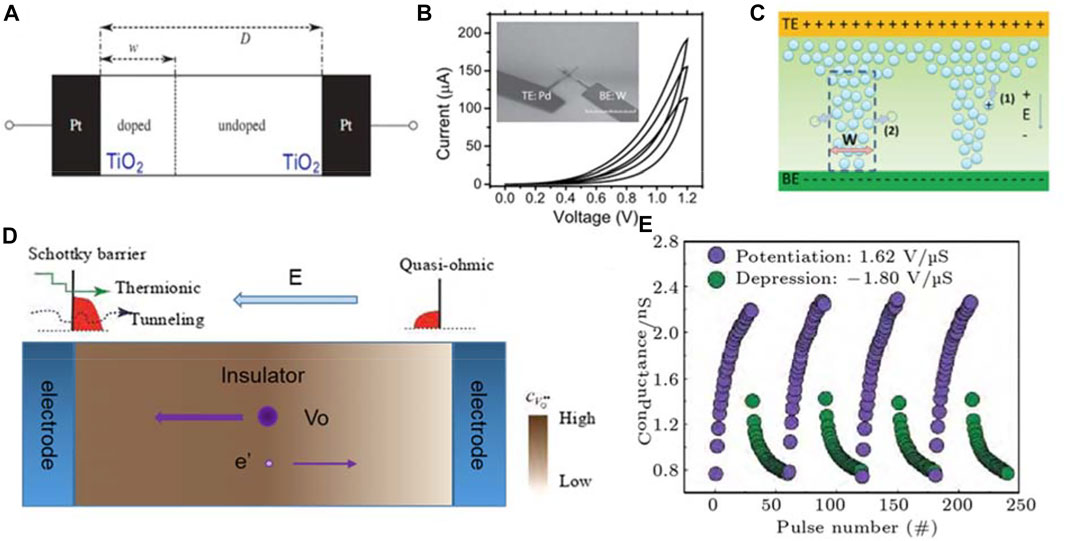
FIGURE 3. (A) The memristive model proposed by HP’s lab. (B) The I-V characteristic of Pd/WOx/W memristor. (C) memtistive mechanism diagram of modulating conductive filaments [43]. (D) Schematic diagram of the memristive model by modulating Schottky barrier. (E) the potentiation and depression of Pt/SrTiO3/Nb-SrTiO3 memristor obtained under positive and negative pulses, respectively [44].
At the same time, doping and the addition of a capping layer can further improve the conductivity tuning linearity of the memristor and adjust the electric field and temperature adaptively [45]. In addition, some complex oxides generally have high dielectric constants, such as PR0.7CA0.3MNO3 [46], SrTiO3 [47], BiFeO3 [48], LaAlO3 [49], and LiFePO4 [50], which can improve the switching voltage, switching ratio, and other parameters. Owing to their high durability, speed, and scalability, and to their mature production technology, oxide memristors have become the most widely used and mature memristor bar array materials.
Two-Dimensional Materials (2DMs)
Compared with traditional materials, two-dimensional graphene has shown excellent electrical, optical, thermal, and mechanical working properties in recent years [51–54]. The development and application of graphene has led to an upsurge of exploration in the field of two-dimensional materials, which are usually crystal materials composed of single layers. The 2D materials currently studied range from conductors and semiconductors to insulators, such as graphene, BN, black phosphorus, transition metal dihalides, and group IV monosulfides [55]. At small sizes, they exhibit excellent non-volatile performance and can be used as excellent memristors. Yan et al. systematically studied the performance of self-assembled low-dimensional PbS as a memristor material (Figures 4A–C), and found that it can effectively guide the penetrating etching path of conductive filaments, improve the uniformity of RS parameters, and improve device performance by reducing the threshold voltage, uniformly distributing the position/reset voltage, improve response time and lower power consumption (Figures 4D–I) [56]. In addition, the two-way conductance can be adjusted by using a graphene oxide device, which proves that the low-energy pulse can realize almost linear conductance regulation. The influence of pulses with different parameters on conductance modulation has been studied, revealing the potential relationship between the pulse amplitude and energy [57–59].
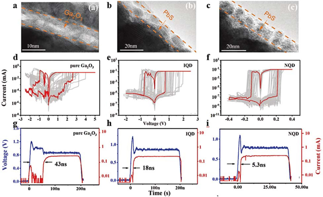
FIGURE 4. Self-Assembled Networked PbS Distribution Quantum Dots for Resistive Switching and Artificial Synapse Performance Boost of Memristors [56]. (A–C) Cross-sectional TEM images of: (A) pure-Ga2O3 MDs, (B) IQD MDs, and (C) NQD MDs. (D–I) Current–voltage (I–V) curves and response time. (D–F) Current–voltage (I–V) curves: (D) Pure-Ga2O3 MDs, (E) IQD MDs, and (F) NQD MDs. (G–I) SET response time for: (G) pure-Ga2O3 MDs, (H) IQD MDs, and (I) NQD MDs. The blue line denotes the input pulse, and the output conducting current in logarithmic scale is represented by red lines.
Two dimensional materials also provide an excellent platform for further research and development of photonic memristors. Abundant material types cover a wide range of electromagnetic spectra, from ultraviolet to infrared. Therefore, 2DMs-based photonic memristors have shown wide applications, such as image sensors for artificial vision [60], optical gating memristors for logical operation [61], and photonic neural networks for neural morphological systems [62]. To date, researchers have widely studied two-terminal photonic memristors and three-terminal floating gate photonic memories based on MoS2 [63], WSe2 [64,65], and BP [66]. Table 1 summarizes the electrical performance and RS mechanism of memristor with different kinds of 2D materials as RS layers in recent years. Studies have shown that the switching mechanism of two-dimensional material memristor can be divided into two categories. One is based on the whole electrode/functional layer, including conductive wires and vacancy wires, while the other is based on the functional layer itself, including charge capture and release, atomic vacancy, etc.

TABLE 1. Summary of electrical performance and RS mechanism of memristors with different with different kinds of 2D materials as RS layers.
The switching mechanism arising from the combinations of the electrode and the functional layer attributes the resistance transition of the memristor to the formation and rupture of the conductive filament. Metal ion filaments are usually formed by the electrochemical reaction of the active electrode under an electric field and subsequent diffusion to the resistive layer, which is named as the electrochemical metallization mechanism (ECM). Figure 5A shows the growth process of the conductive wire in Ag/h-BN/Cu [77]. Ag is oxidized to Ag+ under the forward bias, and Ag+ migrates to the cathode under resulting electric field. Due to the low cationic mobility of H-BN film, Ag+ can easily capture free electrons injected by the cathode, transform to Ag atoms after a short distance migration, and eventually form Ag conductive filaments that show wider cross-sectional area near the Ag electrode, but narrower cross-sectional area at the Cu electrode. Vacancy filaments are formed by the accumulation of original vacancy defects in the functional layer and vacancy generated by ion migration under applied electric field. Hou et al. prepared tubular Ti/H-BN/Cr devices by self-winding technology [71], whose switching behavior was attributed to the formation and rupture of the vacancy wires. As shown in the left portion of Figure 5B, a small number of B vacancies are distributed in the h-BN film in the initial state without external stimulus. When a positive voltage is applied to the Ti electrode, B ions move first near the Ti electrode and leave the B vacancy (middle portion of Figure 5B). Finally, as the applied voltage increases, the B vacancy region grows towards the Cr electrode and forms a conductive filament (right portion of Figure 5B).
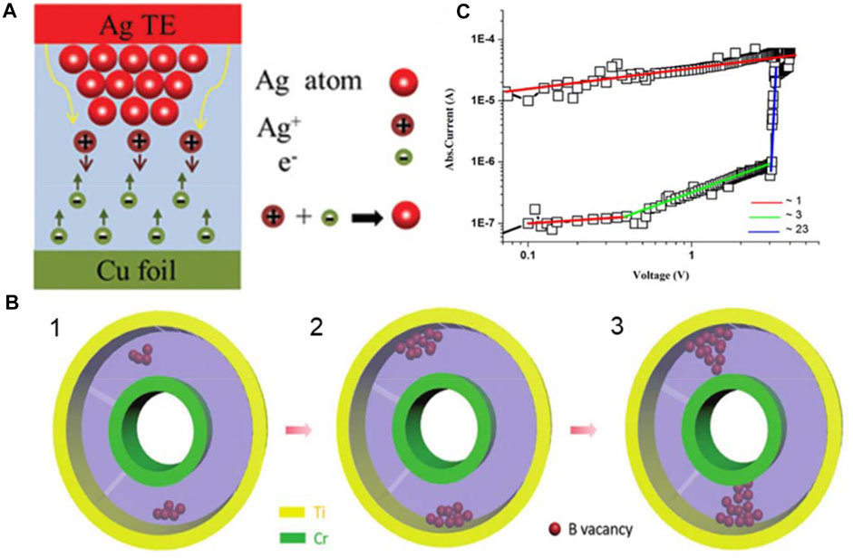
FIGURE 5. (A) Switching mechanism of Ag/h-BN/Cu device [77]; (B) The formation process of the conductive filament in the rolled-up h-BN tube [71]. The internal electrode is metal Cr, and the external is Ti. The red sphere represents the B vacancy; (C) Double Logarithmic I-V curve showing the slopes for HRS and LRS with different values of slope [78].
The switching mechanism stemming from the functional layer only usually refers to space-charge-limited-current (SCLC) mechanism. The memristor devices governed by SCLC mechanism is usually related to the formed traps inside the device. When the carrier is captured by the defect in the medium, the trap energy level distribution in the band experiences the change, and then leads to the resistance transition. Figure 5C shows the I-V curve of Ag/MOS2-PVA/Ag/PET memristor [78], indicating its SCLC-based electronic characteristics [78]. The observed I-V curve is divided into three parts, namely, ohmic conduction, current square and voltage square, after which the current increases rapidly with the increase of voltage. As depicted from Figure 5C, in the low bias region (0–0.4 V), ohmic conduction behavior (slope ≈1) is observed. When the applied bias enters a relatively high region (0.4–3 V), the internal defects in MOS2-PVA composite begin to be filled with charge, thereby increasing resulting conductivities (slope ≈ 3). As the voltage continues to rise, all unoccupied levels or defects are completely filled with charge, whereby the current increases sharply (slope ≈ 23), changing the device resistance from HRS to LRS. Due to the large band gap of the PVA polymer, it is difficult for the charge filled in the defect to return to its original energy state without the help of an external electric field, which makes the device a very high data retention time (105 s).
In spite of its various merits, the two-dimensional memristive materials are still facing severe challenges. Note that the size of the low-dimensional materials is relatively large, which implies a large memristor area using two-dimensional materials. In addition, to realize their industrial application, the large-area controllable preparation technology of two-dimensional materials must be mastered and then transferred to the available substrate. Therefore, the performance reliability of low-dimensional memristors and their material large-area preparation technology is an anticipated area of growth for future research and design.
Ferroelectric Materials
Ferroelectrics are important dielectric materials with a wide range of applications. Because the positive and negative charge centers in ferroelectric materials do not overlap in the cell structure, the electric dipole moment is spontaneously generated and the orientation of spontaneous polarization can be controlled by the external electric field. Because the polarization orientation of ferroelectric materials is irregularly arranged in the initial state, the external macro performance yields a polarization intensity that is equal to zero. Figure 6 shows the relationship between the macroscopic polarization (P) and electric field intensity (E) of ferroelectric materials under the action of an alternating external electric field where the polarization intensity of the ferroelectric material was gradually enhanced. When the electric field is sufficiently large, the polarization intensity reaches its maximum value at saturation. When an electric field in the opposite direction is applied, the polarization intensity gradually decreases to zero. When the electric field is reduced to zero, however, the polarization intensity of the ferroelectric material will not decrease to zero and the polarization residual value will be retained, reflecting nonvolatile behavior.
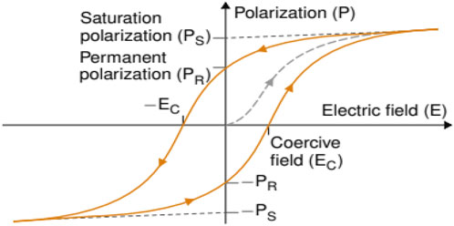
FIGURE 6. Ferroelectric hysteresis cycle: evolution of the overall polarization under an electric field sweep [79].
Studies have shown that the tunnel resistance effect in ferroelectric tunnel junctions triggers a change in the potential energy barrier associated with the polarization reversal of iron [79]. Therefore, the bistable device system can be switched between the open LRS and HRS states with an external bias. In a tunnel junction with a ferroelectric barrier, the switching of ferroelectric polarization will cause a change in the tunnel resistance, and the resistance difference between the ON and OFF states reaches 9, 13, 14, and 15 orders of magnitude. Owing to these large OFF/ON ratios, ferroelectric materials have great application potential in the field of non-volatile storage. In 2012, Chanthbouala et al. proposed a ferroelectric memristor based on a BTO/LSMO structure, which realizes a continuous change in resistance by controlling the domain structure. The ferroelectric domain can be continuously flipped under different voltages, so the device will yield different resistances for different domain structures (Figures 7A,B). Chanthbouala successfully realized the continuous regulation of ferroelectric memristor resistance by changing the amplitude, width, and number of pulse voltage (Figure 7C), as well as the simulation of synaptic LTP and LTD [80]. In 2017, Boyn, S. et al. used the same principle to simulate a biological synapse STDP by using a ferroelectric memristor with a BFO/CCMO structure. The continuous change in resistance was achieved by controlling the domain structure, and the simulation network was formed by using a ferroelectric memristor to build a

FIGURE 7. Tuning resistance and ferroelectric domain configuration with voltage amplitude. (A) Dependence of the junction resistance measured at Vread = 100 mV after the application of 20 ns voltage pulses (Vwrite) of different amplitudes. The different curves correspond to different consecutive measurements, with varying maximum (positive or negative) Vwrite (B) Variation of a similar capacitor resistance with the relative fraction of down domains extracted from the PFM phase images. (C) Tuning resistance by consecutive identical pulses. Evolution of the junction resistance as a function of the different voltage pulse sequences (plotted for Vwrite = +2.9 V and −2.7 V and for Vwrite = +3 V and−3 V).
Conductive filaments formed by oxygen vacancy migration or metal cation migration are random and uneven, which causes large fluctuations in resistance in different regions and affects the accuracy of neural network calculations. Based on the ferroelectric polarization mechanism, the memristor device uses polarization reversal to shift between high- and low-resistance states without heat dissipation and inhomogeneity. Considering that the reversal of the ferroelectric domain will not change abruptly under the action of a single external field, a variety of different polarization states can be obtained with strong controllability by changing the external field voltage. Therefore, the ferroelectric memristor has great potential as a synaptic bionic device, providing opportunities for further research.
Solid Electrolyte Materials
Solid electrolyte, considered as a fast ionic conductor, is usually made of a sulfide electrolyte containing Ag and Cu atoms. Under the applied electric field, the metal cations can migrate out of their original positions and accumulate to form conductive wires connecting the top and bottom electrodes to complete the resistance transition. Such memristor is commonly referred to figuratively as a Conductive Bridging RAM (CBRAM). Note that solid electrolyte is simple in preparation and operation, and is easy to control the formation of conductive wire to construct multilevel resistive memory. However, the resistive memory based on solid electrolyte has unique requirements for electrodes, which generally adopt active electrodes, such as Ag, Cu, etc.
As early as 1976, Hirose et al. studied a memristor device with Ag-As2S3 solid electrolyte material as the functional layer and observed a single Ag conductive filament with an optical microscope [83]. Memristors based on solid electrolytes are usually paired with active metal top electrodes and inert metal bottom electrodes. In these devices, the active electrode can be directly oxidized and reduced by chemical redox reactions, and the generated metal ions can be directly passed through the fast ion conductor matrix by drift and diffusion. This leads to faster switching and lower power consumption. At present, researchers have used GeS2, Ag2Se, Ag-SbTe, Cu-GeTe, Ge2Sb2Te5, and other electrolytes [84–88], and have achieved good experimental results. Erokin’s research group used lithium ion-doped polyethylene oxide as a solid electrolyte to systematically study the influence of electrochemical redox on the electrical transport properties of the store polymer. The group confirmed that metal ions generated by a redox reaction can migrate reversibly between solid electrolyte and polyaniline phases, which allows for non-volatility and for the device to switch between its insulation and conductive states. The three-dimensional network structure of the self-assembled memristor simulates the brain learning abilities of adults and infants [89]. In 2005, Kaeriyama et al. proposed a CuSO4 solid electrolyte nanoswitch, called a nanobridge, which can be used for reconfigurable large-scale integrated circuits owing to its small size and low on-resistance [90].
Manuscript Formatting
Electronic Memristors
The complete electrical concept of the memristor was first proposed in 1971 by Leon Chua and consists of a passive two-ended device whose resistance depends on the amount of charge flowing through it and has a memory effect on the current. Figure 8 shows the relationship between memristors, resistors, inductors, and capacitors, which constitute four basic dual-end passive devices in circuits [91]. It can be seen from the figure that resistance, R, inductance, L, capacitance, C, and memristor, M, can be expressed as the current, voltage, charge, and electric flux. The memristor, M, is expressed by the charge and electric flux as
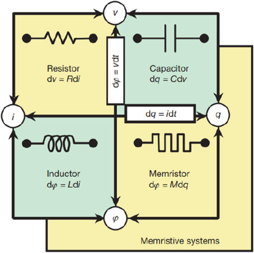
FIGURE 8. Four basic double-ended circuit elements: resistance (R), capacitance (C), inductance (L), and memristor (M) [42].
In 2008, the Williams team of the Hewlett-Packard Laboratory made the first memristor, which has a typical “top electrode/resistive layer/bottom electrode” sandwich structure and proposed a corresponding physical model of the memristor. As shown in Figures 9A,B, in addition to both ends of the electrode, there is only one resistance layer and the resistive switching material, TiO2, is divided into the doped area and the undoped area. The resistance of the doped region is
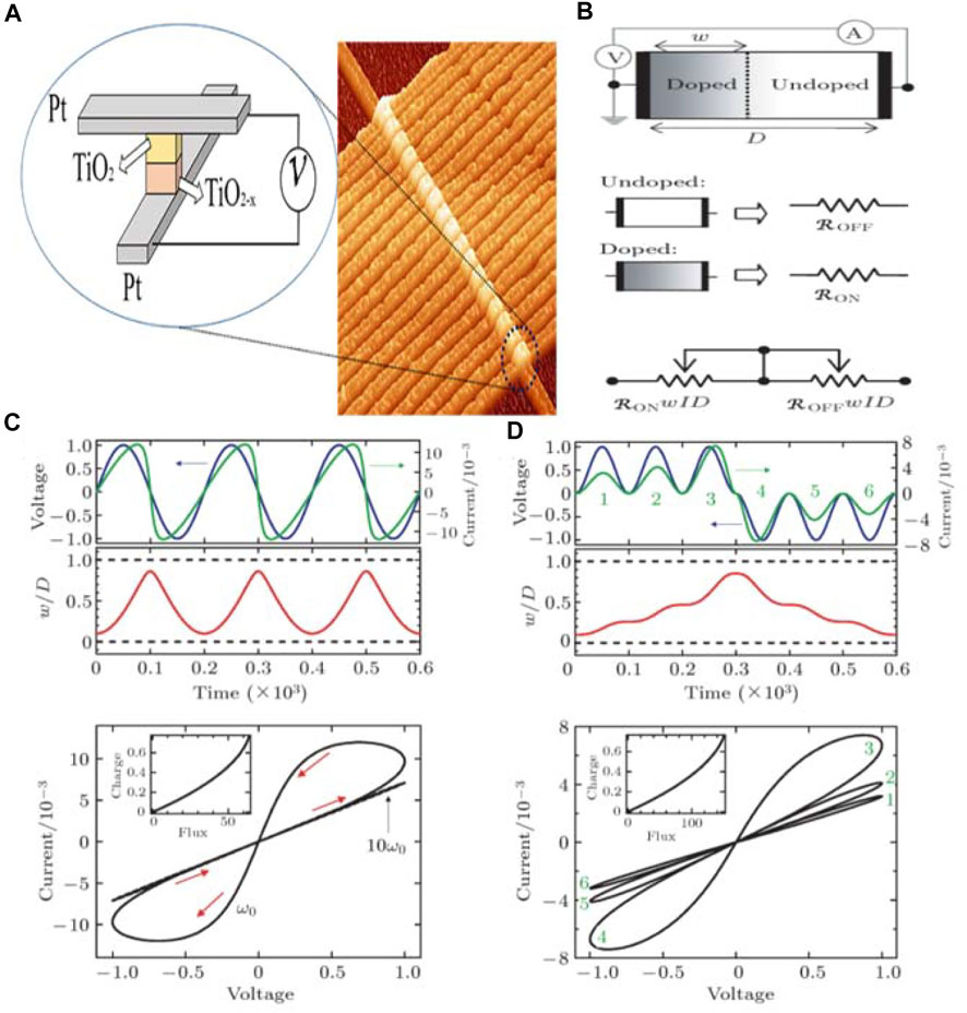
FIGURE 9. Memristor structure and its physical model and memristor resistance hysteresis curve [42] (A) memristor structure diagram. (B) Physical model of the memristor. (C) Symmetrical scanning. (D) Asymmetric scanning.
Photonic Memristors
Inspired by photogenetics, optical signals are included in the category of simulating biological synaptic functions. Researchers have proposed the concept of a photonic memristor, which is a device that uses photonic signals as the excitation source. Under optical excitation, the photonic memristor undergoes resistance switching behavior [92]. Compared with traditional electrical and chemical methods, photogenetics can manipulate biological behaviors with a higher spatiotemporal resolution. Because the beams do not interfere with each other in the three-bit space, the photonic system can provide a higher bandwidth and transmission speed than the electronic system. Moreover, with the expansion of the scale of neural networks, a fully interconnected network consisting of
In recent years, two-dimensional materials (2 dm) have emerged as resistive switching materials, providing a feasible method for preparing ultrathin memory synapses. Recent studies have found that some two-dimensional materials and their hybrid heterostructures, such as half-metallic graphene, insulating hexagonal boron nitride, semiconductor transition metal dihalides (TMD), black phosphorus (BP), and group IV monosulfide compounds (such as SnS2, SnSe, GeSe, and GeS) [93–97], are ideal platforms for non-volatile photonic memory. Moreover, owing to its characteristics, the 2D material has a strong light-matter interaction and its large surface area can produce the trapping ability of obvious photogenerated charges. The atomic thickness of 2D material can further reduce device size and allow the entire column of high-density cross to significantly expand the equipment size. Under the excitation of light, the electronic structure of memristive materials changes to varying degrees, resulting in different resistive switching behaviors. Systems based on different materials have different light-induced resistance switching mechanisms. As shown in Figure 10, the resistance switching mechanism of the photo-induced photonic memristor can be divided into four primary types [92]: 1) photo-induced Schottky barrier, 2) photo-induced conductive filament formation/rupture, 3) photogating, and 4) photo-induced conformation change. At present, photonic memristors are mostly used in image sensors for artificial vision and optical gating devices for logic operations. Photonic memristors are expected to be used to build photonic neural networks for neural morphological systems, which are also attracting more attention.
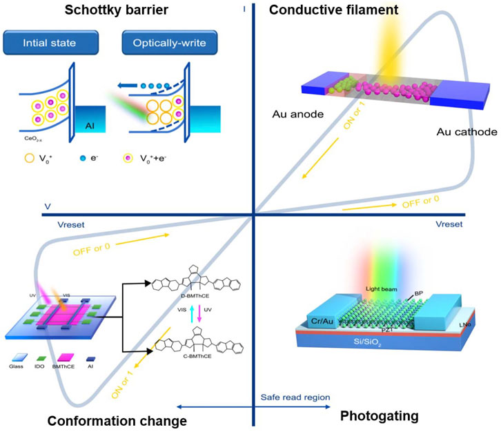
FIGURE 10. Classification of optical memristors, including Schottky barrier (top left), conductive filament (top right), conformation change (bottom left), and photogating (bottom right).
Optoelectronic Memristors
As mentioned above, electrical and optical pulses can regulate the characteristics of the material, thus forming electrically and optically stimulated memristors, and their differences from purely photonic or electronic memristors are schematically described in Figure 11.
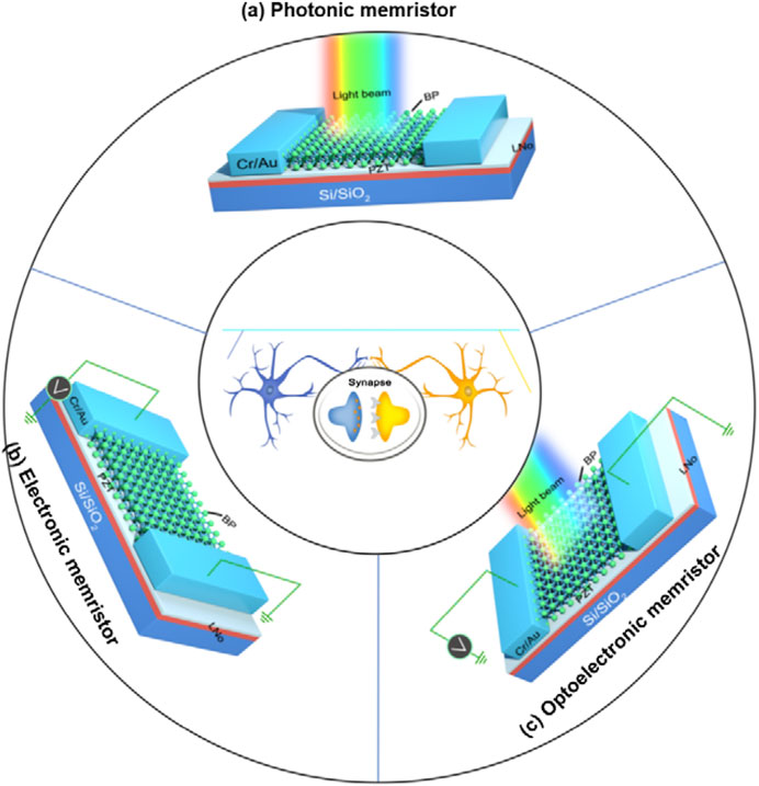
FIGURE 11. Classification of memristors, including (A) photonic memristor, (B) electronic memristor, and (C) optoelectronic memristor.
Optical pulses can not only generate electron-hole pairs, but also regulate the formation of holes or ions in certain materials. In contrast, electrical pulses can induce the movement of carriers and ions. Guo et al. grew ZnO thin films on Al substrates through sputtering deposition. Since Al can capture oxygen in ZnO, a AlOy layer was therefore formed at the interface between the two substrates, and then ZnO1-x/AlOy heterojunction was obtained. This triggered a birth of oxide heterojunction-based a photoelectric synapse (Figure 12). Such device exhibits slow memristive switching characteristics and persistent photoconductivity, consequently mimicking the plasticity of various synapses under external optical stimulus. The device was found to exhibit a persistent photoconductivity under 310 nm UV light, which is ascribed to the accumulation and trapping of optical carriers at the ZnO1-x/AlOy interface for a built-in electric field. When UV light is irradiated, the photogenerated electrons are excited to the conduction band to increase the device conductance. Thanks to this, the photogenerated holes accumulated continuously at the ZnO1-x/AlOy interface are captured by the AlOy layer under the built-in electric field. When the light is removed, the captured photogenerated holes are difficult to be released in a short time, which further obstructs the recombination with the photogenerated electrons. The device conductance in this case can be maintained for a long time, resulting in a persistent photoconductivity. Figure 12B illustrates such photo-synaptic enhancement and electrical inhibition processes. Under UV pulse irradiation, the device conductance increases with time, corresponding to the LTP behavior. With the application of the electrical pulses, the device conductance decreases continuously over time, corresponding to the LTD behavior.
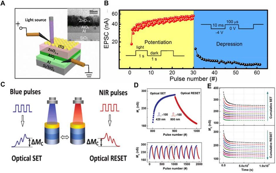
FIGURE 12. (A) Structural illustration of memristive device based on ITO/ZnO1-x/AlOy/Al, and the corresponding transmission electron microscope (TEM). (B) Photonic potentiation and electrical depression of stimulated pulses-dependent EPSC [98]. (C) Working mode of all-optically controlled memristor based on IGZO; (D) Reversible regulation characteristics of conductance (upper) and cycle stability (down); (E) Retention characteristics of memconductance states after optical SET (upper) and optical RESET (down) operations [99].
When light regulation is introduced into the memristor as an additional dimension of the control method to regulate the evolution of the conductive filaments or interface barriers, device conductance can be modified by the pure optical means with different wavelengths and illumination intensities, thus achieving a synergy between light and electric fields. Zhu et al. prepared an Au/OD-IGZO/OR-IGZO/Pt all-optical memristor by using IGZO, a four-element oxide semiconductor material with relatively mature preparation technology, and successfully simulated its synaptic function. The conductance regulation mechanism of an all-optical memristor is derived from the reversible change of the barrier width at the interface of photoinduced bilayer oxides. When the short wave light is applied, the ionization of oxygen vacancy plays a dominant role, which increases and narrows the concentration of ionized oxygen vacancy and the interface barrier, respectively. Resulting current and device conductance are subsequently increased. The neutralization effect of oxygen vacancy is however stronger than that of ionization when long wave light is applied. This oppositely decreases the concentration of ionized oxygen vacancy, broadens the interfacial barrier, and reduces the conduction current. The working mode of all-optically controlled memristor is shown in Figure 12C where reversible transitions from low conductance states to high conductance states and vice versa are realized under blue and near infrared light pulses, respectively. In Figure 12D, the stable and reversible transformation process of the device conductance by controlling the external optical stimulus is shown, which increases the conductance under the 420 nm light pulse and decreases the conductance under the 800 nm light pulse. Besides, the device has good non-volatile property and its different conductance states can clearly be distinguished from each other after 104 s (Figure 12E).
Both optical and electrical pulses can enable the phase transformation of the well-known phase-change materials (i.e., chalcogenide alloy). In addition, electric pulses can induce the polarization of the ferroelectric materials, and light pulses can generate the photocurrent responses owing to the photovoltaic effect of the ferroelectric materials [99]. These conditions promote the development of optoelectronic devices using the synergistic effect of light pulses and electrical pulses to control the electrical properties of the device. Optoelectronic memristors are considered to be promising candidates for multi-functional neural morphology computing (especially artificial vision systems) because of their ultra-fast operating speed, almost unlimited bandwidth, avoidance of crosstalk interference, elimination of Joule heating, and the potential for functional integration involving optical signal sensing, processing, and storage in a single unit [100,101].
Memristor Neural Networks (MNNs)
Based on the physical characteristics of the memristor itself, if it can be directly used as the weight of the neural network circuit through physical law, then efficient large-scale memory calculations can be carried out by learning algorithms. This will improve the system’s computational, parallel, and adaptive ability and allow the weight value to be retained within the system for a long period after a power outage. Although the energy efficiency and calculation speed of the recently realized MNNs are satisfactory, there are few applicable examples of MNNs. The difficulty lies in discovering how a memristor can understand learning rules other than STDP. Achieving implementation of a memristor-based neural network circuit requires more time.
Artificial Neural Networks (ANNs)
An artificial neural network (ANN) is a network widely interconnected by many processing units (neurons) that mirrors a biological neural network allowing researchers to better understand and imitate human capabilities by replicating the basic characteristics of the human brain through abstraction, simplification, and simulation. It is a computational model based on the structure and function of a biological neural network, which has information processing, learning, and storage functions similar to the human brain and exhibits the natural characteristics of storing and applying experiential knowledge. ANN and the human brain are similar in two primary ways: they acquire knowledge from the external environment through the learning process and then use their internal neurons (synaptic weights) to store the acquired knowledge.
The mathematical model for the first generation of ANNs was first proposed by Warren McCulloch and Walter Pitt in 1940. Known as Perceptron, it is one of the simplest neural networks [102]. In 1957, Frank Rosenblatt proposed a computer-based programmable method to simulate human perception [103]. Perceptrons are based on biological neural networks and strictly correspond to many concepts in biology. Perceptron inputs can be a series of integers, mathematical vectors, voltages, or currents. Signal transmission and processing of axon function in the neurons of neural networks are achieved by the weighted summation of inputs. The output is generally a number or vector depending on the needs of different networks and bionic environments.
After Perceptron was first used to implement the algorithm on transistor-based computers, Rosenblatt et al. first implemented the algorithm on an IBM 704 computer in 1957 to identify multiple image sets composed of 400 pixels. The weight was expressed by potentiometers and motors [104]. Although the described calculation is still based on the immature computer technology of that time, the use of variable resistors as weights is very close to the essence of the memristor rod structure. Neurons preserve information in neurosynapses. This preserved information, specifically, the weight, affects the connection strength of neurons before and after. In traditional computer information storage, the weights of neural networks are stored in the form of an N-bit binary. In contrast, only a single memristor can represent a weight in neural network design, which uses the memristor’s simulation characteristics of learning and memory functions to achieve network computing. The main principle for realizing the inductor in the circuit is shown in Figure 13. The input signal is represented by the voltage, and each input voltage corresponds to multiple memristors. For short and stable relative voltage, the resistance value of the memristor remains unchanged. According to Kirchhoff’s current law and Ohm’s law, each output multiple corresponds to the memristor column, and the outflow current is superimposed onto the output port to achieve the weighted sum. The memristor achieves the weighted value through changes in conductance, which is aligned with the final activation function. The output current is processed to obtain the required output using analog equipment.

FIGURE 13. Mathematic model and memristor realization of single-layer perceptron. (A) mathematic model of single-layer perceptron. (B) schematic of SLP memristor realization.
Training learning is also an important part of artificial neural network research. The adaptability of the neural network is realized through training. The main learning method is to construct reverse propagation and constantly change the weight to improve the accuracy of the ANN. According to the different learning environments, ANN learning methods are divided into supervised and unsupervised learning.
In supervised learning, the sample data are input into the network, and the expected value of the network output is given. The network output results are continuously compared with the expected output. After the training, each neuron converges to a weight, and the optimal solution for the neural network calculation is realized.
Unlike supervised learning, unsupervised learning networks do not know whether their classification results are correct or not. Only input examples are provided to the network, which automatically finds potential category rules based on these examples. When learning is over and tested, the results are used for new cases.
Perceptron is the origin algorithm of neural networks and uses supervised learning. Prezioso et al. (2015) constructed a nine-input, one-way bias and three-output perceptron network using a Pt/Ta/Ti/TiO2-x/Al2O3/SiO2/Si structure to construct a
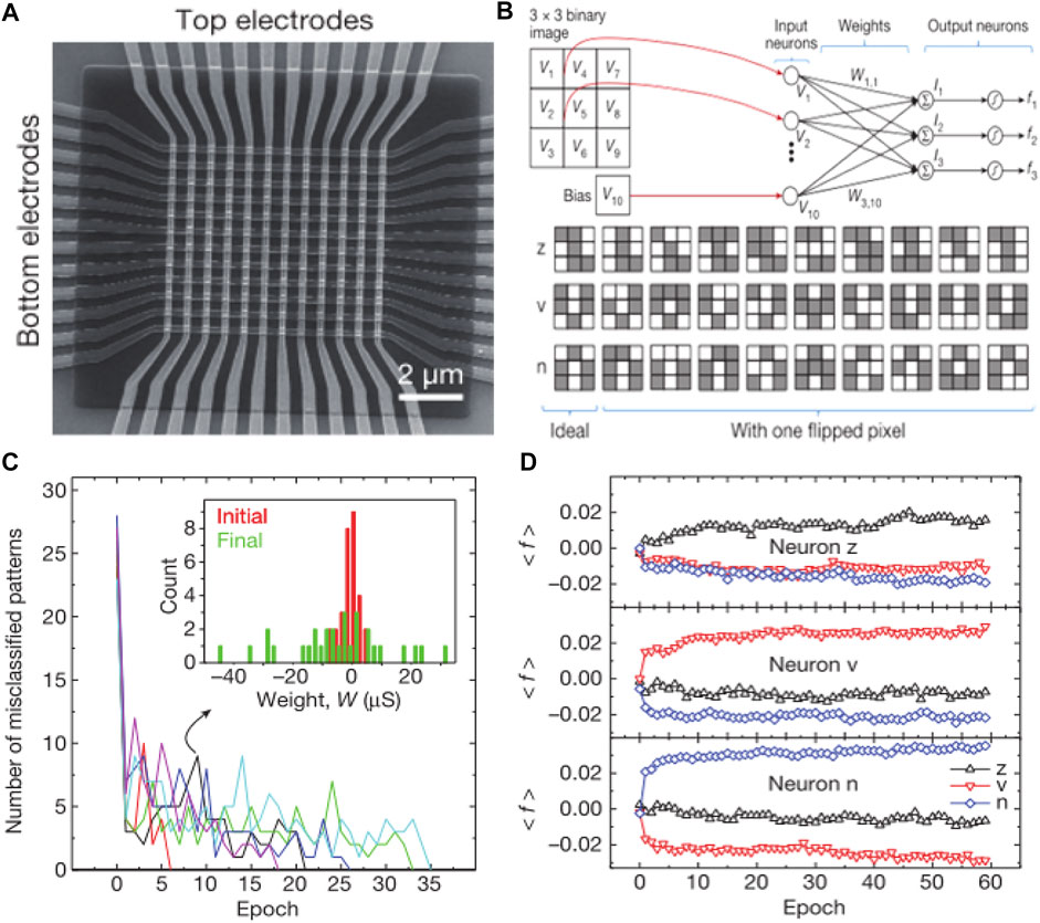
FIGURE 14. A 12 × 12 transistor-free memristor crossbar neural network [105] (A) Integrated 12 × 12 crossbar with an Al2O3/TiO2-x memristor at each crosspoint. (B) The single-layer perceptron for classification of 333 binary images and used input pattern set. (C) Convergence of network outputs during the training process to the perfect value (zero) for six training runs from different initial states. (D) The evolution of output signals, averaged over all patterns of a specific class.
Deep Neural Networks (DNNs)
DNNs, also known as deep learning, are algorithms used in machine learning, which are based on data representation. The depth of deep learning is achieved through several hidden layers with more complex selection problems requiring more hidden layers. Primary perceptrons can only solve simple recognition and classification problems based on existing features – using them to solve complex problems is still a challenge. To address this problem, a deep-learning algorithm was developed for the perceptron based on a deep neural network (DNN). Deep-learning frameworks comprise a large group and include systems that have been applied in computer vision, speech recognition, natural language processing, audio recognition, and bioinformatics to achieve excellent results [107–111]. A primary sensor memristor can also be used in a DNN, which updates the synaptic weight by continuously renewing the conductance value of the memristor through supervised learning to achieve different algorithms. This chapter introduces three types of deep neural network models implemented with memristors: the multi-layer perceptron (MLP), the convolutional neural network (CNN), and the recursive neural network (RNN).
Multi-Layer Perceptron (MLP)
The primary perceptron is essentially a single-layer system with limited functionality. To transcend these limitations, we developed a deep learning neural network model based on the primary perceptron referred to as a multi-layer perceptron (MLP). The MLP is a neural network with a forward structure that maps a set of input vectors to a set of output vectors. As shown in Figure 15, an MLP can be seen as a directed graph composed of multi-layer nodes, with each layer node fully connected to the next layer. The MLP can be understood as the superposition of multiple single-layer perceptrons, with the output of each layer acting as the input of the next layer. Apart from the input node, each node is a neuron (or processing unit) with a nonlinear activation function. The network structure, shown in Figure 15, is divided into input, hidden, and output layers. Learning is a two-step process that includes identification and training. Identification consists of the forward propagation process and training includes the error back-propagation process combined with the output results of forward propagation at each layer. When the network is trained to be stable and possesses the required identification accuracy the network ceases to update for identification, which is referred to as offline identification. However, MLPs are not strictly perceptrons. A real perceptron is a special case of artificial neurons using a threshold activation function, such as a step function, while an MLP can use any activation function. A true sensor performs binary classification, whereas an MLP neuron can freely perform classification or regression according to its activation function [112–114].
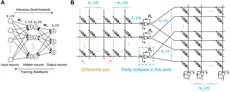
FIGURE 15. Mathematic model and memristor realization of a multilayer perceptron [107]. (A) mathematic model of MLP (B) schematic of MLP memristor realization.
The memristors in MLPs have multi-order characteristics that are analogous to synapses in neural networks that store the synapses’ weights. Conversely, memristor arrays, which are used for MLP acceleration, are based on multi-order characteristics and can execute parallel weighted summation operations (matrix vector multiplication), which are the most time-consuming steps in most neural network algorithms. Large-scale parallel matrix vector multiplication can be achieved by mapping the neural network weight matrix to the conductance in the memristor array. Thus, parallel write-by-line or write-by-column operations (weight update) can be performed in memristor arrays, whereas the synaptic arrays constructed by traditional SRAM devices can only write serially. The introduction of a memristor greatly improves the training speed of the neural network algorithm. Based on the memristor of a ferroelectric material, Djaafar Chabi et al. (2015) constructed a three-dimensional architecture of the memristor computational model to achieve the three-layer perceptron algorithm, which was successfully implemented using a simulation for nonlinear differentiable functions. After simulation testing, real devices were fabricated and used to implement the corresponding multilayer perceptron algorithm [115]. Farnood Merrikh Bayat et al. (2017) constructed
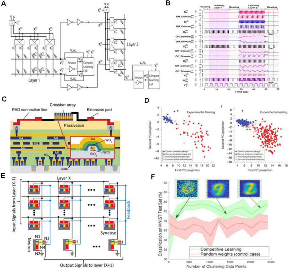
FIGURE 16. Memristor realization of a multilayer perceptron and its applications. (A) Architecture of a multilayer neural crossbar for ultra-high-density on-chip learning using analog FTMs as synapses and binary FTMs to implement the learning cell. (B) Electrical simulation results of a multilayer compact neural crossbar demonstrating the learning of a 2-input XOR-function [116]. (C) Cross-section schematic of the integrated chip, showing connections of the memristor array with the CMOS circuitry through extension lines and internal CMOS wiring. Inset, cross-section of the WOx device. (D) Classification results experimentally obtained from the memristor chip for the training and testing data. Blue and red dots represent the predicted benign and malignant data, respectively. The incorrectly classified results are marked as open circles. Classification rates of 94 and 94.6% are obtained for the training and testing data, respectively [117]. (E) 3T DW-MTJ synapses arranged in a crossbar architecture. (F) Test set classification on the MNIST dataset is given as a function of datapoints presented to the system learning with clustered weights (green); as is visible, this approach converges quickly and outpaces the constant weights system (red) not benefiting from this operation [118].
The MLP is a general neural network. In addition to research on the classification and design of linear differentiable problems, most of the multi-layer neural networks derived from the perceptron are dedicated neural networks, such as CNNs and RNNs.
Convolutional Neural Network (CNN)
When faced with complex image problems, the MLP neural network has the disadvantages of slow calculation speed and large consumption. As a result, convolutional neural networks, CNNs, are commonly used to deal with computer vision problems such as image classification and recognition and, owing to their weight sharing and local connections, are preferred for processing images. As shown in Figure 17, the CNN consists of one or more convolution layers and a vertex fully connected layer (corresponding to the classical neural network), which also includes relevant weights and a pooling layer. This structure allows the CNN to utilize the two-dimensional structure of the input data. The CNN first extracts the features of the input image through several convolution and pooling layers, and then outputs the network processing results through the full connection layer for classification.

FIGURE 17. Mathematic model of CNN [119].
The convolution layer is the most critical component of the CNN and is defined by the number and size of the convolution kernels, convolution step size, input image size, and other parameters. In image recognition, convolution is two-dimensional. The convolution kernel covers the same size area as the image and performs the inner product operation using the pixels within the area. Different convolution kernels can obtain the same number of feature maps to extract multiple feature maps. Sharing weights through a convolution kernel reduces the number of parameters that the network needs to train.
Second, to reduce the size of the model and improve the operation speed, the pooling layer downsamples the feature map extracted from the convolution layer to obtain a new feature map. Pooling is divided into mean pooling, which averages the values in the calculation area of the input image, and maximum pooling, which takes the maximum value in the area to obtain a new feature map.
The input image is extracted twice by the convolution and pooling layers, and finally by the fully connected layer. The connection mode of the fully connected layer is the same as that of the perceptron neural network. Each neuron is connected to the neurons in the upper layer and has its own weight parameter, w, which plays a classification function.
Finally, the output of the fully connected layer is processed through the output layer. The output layer is generally an activation function for classification problems, including the radial basis function (RBF), sigmoid function, and softmax function. The sigmoid function is mostly used for binary classification problems, while the softmax function can perform multi-classification processing. The output of the full connection layer is processed by the activation function in the output layer, and the identification results of the network are finally output.
In CNN, the memristor is used as the storage medium via its simulation characteristics, with a single memristor used to represent a weight. The memristor primarily plays the role of a nerve synapse, and the realization method is the same as that of a single-layer perceptron. For example, Nourazar et al. (2018) constructed a model based on the general-purpose Hewlett-Packard memory. A CNN with a resistor model was simulated using an x86 processor and open-source C++ code. The network implemented the multiplication of
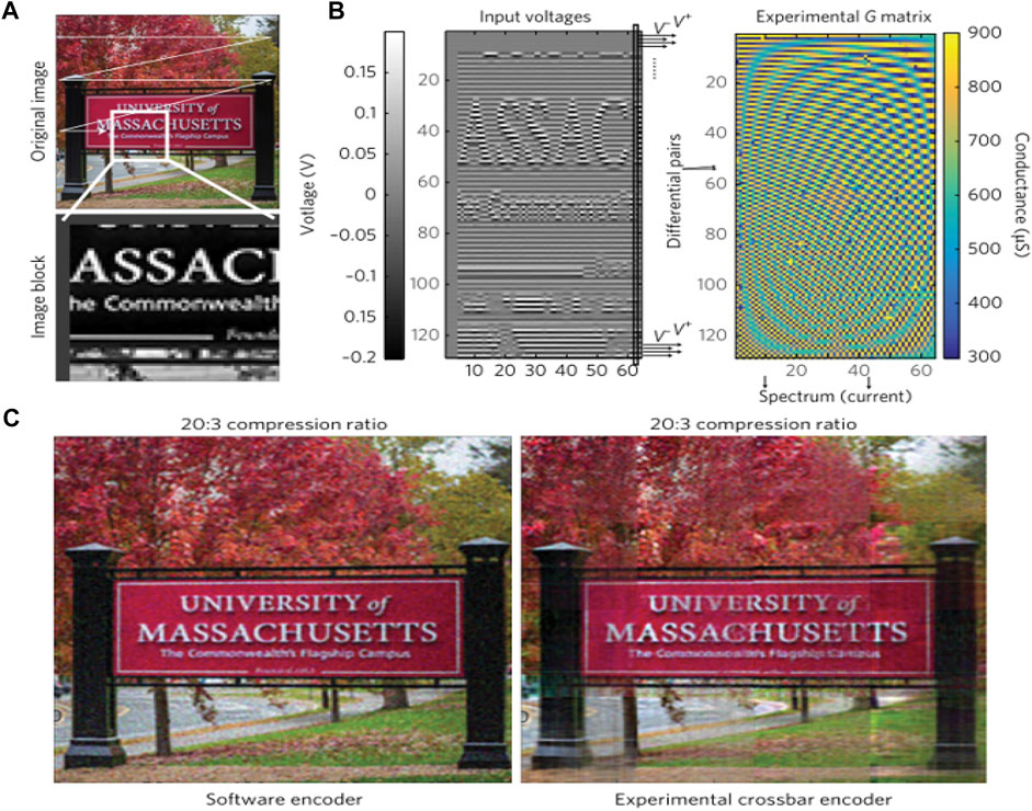
FIGURE 18. Experimental 2D DCT demonstration using differential conductance pairs for image compression and processing [121]. (A) The original image for compression was input into the crossbar block by block for the 2D DCT. (B) The image block was converted to voltages that were applied to the row wires of the crossbar (left), with neighboring wires having a voltage pair with the same amplitude, representing image pixel intensity, but opposite polarity. To the right, a differential DCT written into the 128 × 64 array, with the small number of stuck “on” or “off” memristors evident as disruptions in the pattern. (C) Images decoded from the 2D DCT by software (left) and experimentally (right). Before decoding, only the frequencies representing the top 15% of the spectral intensity were preserved (a 20:3 compression ratio).
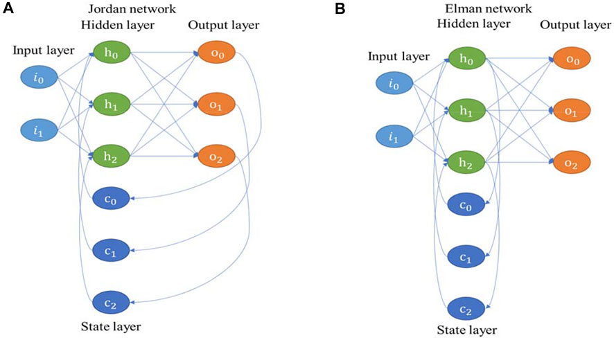
FIGURE 19. Mathematic model of two kinds of RNN. (A) Jordan Recurrent Neural Network (B) Elman Recurrent Neural Network.
Recursive Neural Network (RNN)
A recursive neural network (RNN) consists of fixed weights, external inputs, and internal states, which can be regarded as the behavioral dynamics of internal states with weights and external inputs as parameters. RNNs are classified as time RNNs, which have inputs that consist of a time-related sequence and with connections between neurons that constitute a directed graph, and structural RNNs, which are neural networks designed in a structure. A similar neural network was recursively structured to construct a complex network. Most connections between neurons constitute an undirected graph and the neural network is independent of the input. The structural RNN can be developed into a time RNN through effective improvement. Hopfield neural networks and BAM neural networks are common structural RNNs. For the time RNN, the traditional RNN structure diagram shows the input of the neurons in layer
Based on the HP memristor-based model and Chua’s development of memristor theory, Wu et al. (2012) simulated a hybrid Lotka Volterra RNN with conditions sufficient for nondivergence and global attractivity. The results are applicable to memristive dynamic memory [125]. Gang Bao et al. (2014) designed an RNN based on the HP memory block model of the back-to-back structure of memory block networks, which can be adapted to the desired neural network based on the requirements of the application. By constructing appropriate Lyapunov-Krasovskii functionals and using the characteristic function technique, the structure presents new theoretical results on the passivity and passification of a class of memristor-based RNNs (MRNNs) with time-varying delays where passivity conditions are cast in the form of linear matrix inequalities (LMIs) that can be verified numerically using an LMI toolbox [126]. These theoretical studies laid the foundation for real memristor implementation of RNNs.
A real RNN based on a memristor consists of two cross structures. One is used to extract the main features of the subject from multiple continuous images or short videos, and the other is used to classify the subjects according to the features extracted from videos or photos. Li et al. (2019) implemented long short-term memory memristor RNNs based on the Ta/HfO2 crossbar array architecture, where one was used to implement a recurrent network and another was used to recognize the number of features extracted from the RNN, as shown in Figures 20A–C. This network was used to identify people’s occupation based on their biometric features, including their height and waist circumference, and based on their behavior, such as walking or standing still. The information was extracted from videos based on a sequence of picture [127]. When used for image recognition, purely cyclic neural networks exhibit limitations related to the accuracy of feature extraction and stability of operation; thus, a hybrid CNN for cyclic neural networks has been creatively implemented in memory blocker-based neural networks. To classify the MNIST dataset, Zhongrui Wang et al. (2019) built the in situ training of a five-level CNN with non-idealities of a one-transistor one-memristor (1T1R) array (Figures 20D,E) and achieved similar accuracy to the memristor-based multilayer perceptron [128]. These principles proved that a hybrid CNN can combine the structural advantages of weight sharing and the area/energy efficiency improvements of memristors, paving the way for the future of edge AI.
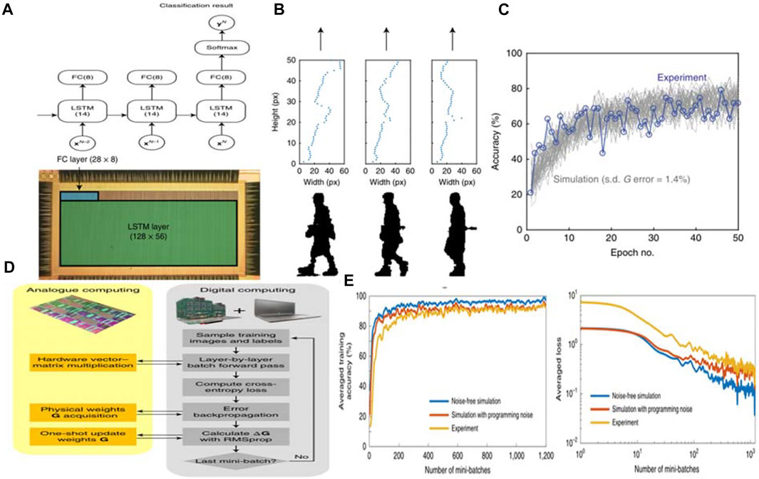
FIGURE 20. Classification experiment for human identification by gait [127] (A) Two-layer RNN configuration for classification and Partition of the 128 × 64 1T1R memristor crossbar array, in which a 128 × 56 sub-array is used for the LSTM layer and a 28 × 8 sub-array for the fully connected layer. (B) Elman Recurrent Neural Network. (C) Width profiles of the human silhouettes are extracted from a video as the inputs for the RNN. In situ training of the 1t1R-based five-level CNN [128]. (D) Schematic of the hybrid analogue–digital training of the CNN. (E) The smoothed experimental in-batch accuracy increased and loss decreased over the course of in situ training. The experimental curves are indistinguishable from the simulation that includes programming noise, closely following the defect-free simulation with a ∼4% gap in accuracy during the second epoch of the training.
Spiking Neural Networks (SNNs)
According to neuroscience research, many biological nervous systems, such as vision and hearing, are encoded in the form of pulse duration. Based on this background, a more biologically authentic pulse neural network (third-generation artificial neural network model) has been developed. To achieve efficient information processing, SNNs transmit and process information through time coding; thus, modeling a biological nervous system more accurately than first and second generation ANNs. SNNs use biologically oriented pulses (action potentials) to transmit information between synapse-connected neurons. Recently, influenced by the success of DNNs, people have become increasingly interested in using SNNs to complete specific tasks [129]. SNN simulation is usually divided into two stages - neuron calculation and pulse propagation - and each stage is defined by the neuron/synapse model. The membrane potential accumulates after the neurons receive the pulse sequence. When the membrane potential of the neurons exceeds the threshold voltage, a pulse is emitted, the membrane potential is reset, and the pulse signal is transmitted to the next neuron through the axon. In SNN, to simulate the behavior of real neurons, several spike neuron models with biological characteristics of STDP learning rules have been proposed. The commonly used neuron models are–the Hodgkin Huxley (HH) model [130], the Integrate and Fire (IF) model, the Leaky Integrate and Fire (LIF) model [131], and the Izhikevich model [132]. The physiological model represented by HH is closer to biological action characteristics and is more aligned with electrophysiological characteristics of neurons. The model, however, is complex and requires significant computation, making it difficult to apply to large-scale circuits. LIF and IF models are behavior-level models that do not accurately describe the biological characteristics of neurons, but simulate their action characteristics. Thus, reduced accuracy yields a model with fewer computational requirements, making LIF and IF models more common in SNN. The current state of the neuron is defined in SNN as its activation level (modeled as a differential equation). The input pulse causes the activation level in a neuron to rise over a period of time and then gradually decline. Considering the pulse frequency and interval, a coding scheme can be constructed to interpret these output pulse sequences as numbers, indicating that it is possible to establish an accurate neural network model based on the starting time of the pulse. With an accurate pulse starting time, a neural network that adopts peak coding can access more information to provide more powerful computing.
At present, research based on pulse neural networks in China and abroad is more extensive than research based on other types of ANNs. For example, Nishitani et al. proposed a supervised learning model that allows error back propagation for a pulse neural network and used a memristor as an electronic synapse to store simulated synaptic weights. An online supervised learning algorithm was applied to a pulse neural network based on a memristor and managed classification tasks well. There are two types of bio-inspired FDCs that are based on the memristor and the BSIM3V3.2.2 transistor model (Figure 21B), which can simulate the behavior of the synapse and neuron discharge, and can detect faults when the measured element is damaged [133]. Errui et al. proposed a highly integrated hardware implementation of memristor-based SNNs with pulses that are simplified as step signals [134].
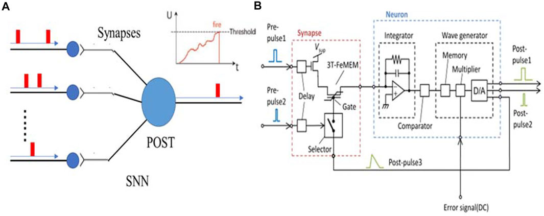
FIGURE 21. (A) A LIF spiking neuron model. (B) Example of 3T-FeMEM based synapse and LIF neuron circuit [133].
In principle, SNNs can be applied to the same applications as traditional artificial DNNs and beyond, including the central nervous system of biological organisms. However, owing to the lack of an effective SNN training mechanism, SNNs are not conducive to some applications. Using image processing as an example, the traditional DNN converts the image into a voltage signal according to the color and brightness of the image, while the SNN converts the image into a time-span pulse signal. This presents a very complex problem when using SNNs to process a photograph taken with a camera, but SNN can easily process a picture taken by a closed-circuit television. Moreover, a lack of further understanding of SNNs means that pure SNN is currently difficult to implement through memristor-based circuits.
While the hardware implementation of SNNs currently presents challenges, the implementation of some ANNs is relatively easy. Recently, Rivu et al. designed an ANN-SNN converter (Figure 22 by using diffusion memristors and shunt capacitors. This is equivalent to the value of neurons in a traditional ANN, which is used to encode the peak frequency, and is the method available at this stage to build an SNN using memristors [135].
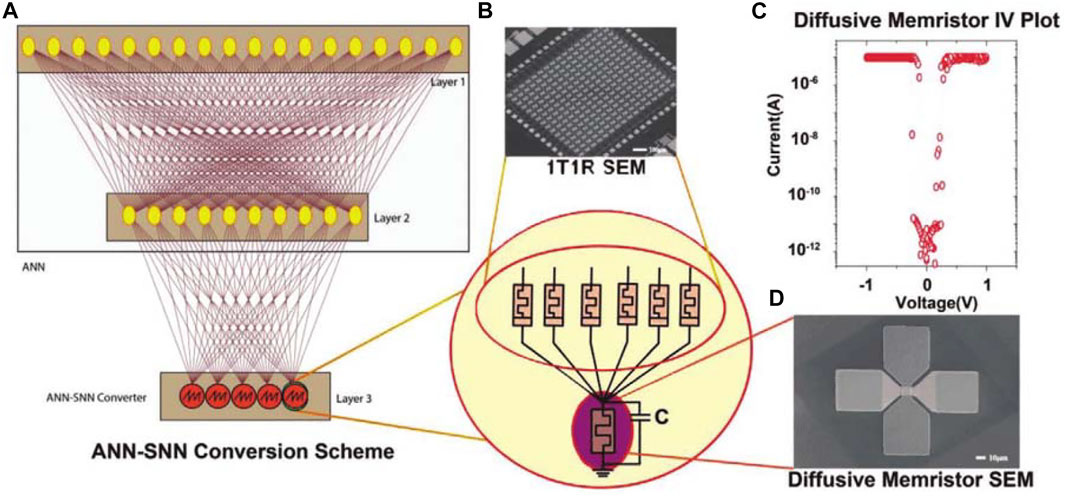
FIGURE 22. ANN–SNN conversion scheme [136]. (A) An ordinary two-layer ANN and a third-layer oscillatory neuron. (B) SEM image of ANN. (C) The I–V curve of a memristor used to create an oscillating neuron. (D) SEM image of diffused memristor.
Photonics-Based Neural Networks
It is necessary to point out that most of the neuromorphic devices are driven by the electrical stimulus. In comparison with the electrical stimulus, light has the advantages of ultra-high speed, wide band width and low crosstalk. Optogenetics studies show that light can also effectively regulate brain behavior [137], which also lays a biological foundation for the construction of the photoelectric neuromorphic system. For the photon and photoelectric memristors, the adjustable conductance of the memristor is used as the synaptic weight, and the photon or electrical stimulus is used as the synaptic peak. Photonic memristor can directly sense the external light stimulus and complete information processing in the photoelectric conversion process. This integrated mode of information perception and processing is very similar to the human visual system. Therefore, the applications of the photoelectric neuromorphic devices are mainly focused on the artificial vision systems. Compared with the artificial vision systems using electronic memory elements, artificial vision systems with photonic memristors have great potential in constructing artificial vision systems. The human visual system consists mainly of the eyes, the lateral geniculate nucleus (LGN) and the visual cortex. The retina first captures light, preprocesses and prepares the information, and the extracted information is then transmitted through the optic nerve to the visual cortex for processing. The cone in the human eye provides color vision by absorbing spectral radiation based on wavelength (red, green, blue). Similar to the human visual system, the photonic synapses not only respond directly to light stimuli, but also have data storage and visual information processing capabilities. For the development of the artificial vision systems, photonic neural networks show great potential in image perception, image memory, color discrimination and real-time preprocessing, which further lower the hardware and power consumption. Seo et al. [138] fabricated an optoelectronic synergistic synaptic device by integrating the synaptic devices and light sensors on the same h-BN/WSe2 heterostructure (Figure 23A). Such device responds differently to the wavelength of red (R), green (G) and blue (B) light. The team utilized O2 processing to capture and release electrons in the weight control layer (WCL) formed on h-BN to achieve synaptic structure. Figure 23 shows the synaptic weights of the optical neural network after the 12th and 600th training epochs, indicating the influence of the calendar element on the recognition effect. The optical neural network successfully realized the recognition task of the color and color mixed number (1 and 4), and the recognition rate reached 90%. It has important application potential in color mixed number recognition based on the photoelectric synapse devices. In addition, Wang et al. designed an artificial vision neuron which was connected in series by IGZO4 UV sensor and NbOx oscillating neuron, and successfully constructed a Spiking neural network [139]. Such device structure is shown in Figure 23C. The proposed device can not only sense the UV light but also encode the light information into electrical pulses. The IGZO4 device has good UV response, and the resistance value decreases with the decrease of the UV wavelength. Figure 23D shows the circuit structure of the artificial visual neuron. The device can display four stable peak frequencies when stimulated by the UV light at different wavelengths, as shown in Figure 23E. Based on the artificial neuron, complex background images can be segmented according to different oscillation frequencies, and the information encoding function of the artificial vision system is demonstrated.
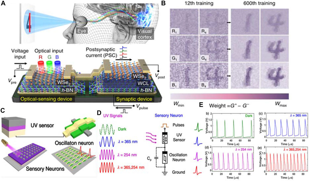
FIGURE 23. Optoelectronic neuron devices. (A) A optic-neural synaptic device based on the h-BN/WSe2 heterostructure. (B) Synaptic values change versus the increase of the training number [138]. (C) Structural illustration for artificial visual neuron composed of IGZO4-based UV sensor and NbOx-based oscillator. (D) Working mode of artificial visual neuron under different light illumination. (E) Four different firing behaviors of artificial visual neuron in dark and upon stimulation with different wavelengths UV light [139].
In addition to the visual system, the human body also has sensory functions such as touch, hearing and smell. In recent years, optoelectronic neuromorphic devices have also received extensive attention in these sensing systems [140–143].
Summary and Outlook
The birth of memristors has vigorously pushed forward the development of AI technologies. Its analogous characteristics to the biological brain mean that it will likely bring to fruition in the near future the dream of machines that think and behave like humans. As photonic memristors are in their infancy, electronic memristors, primarily represented by resistive random-access memory, are the key components of memristor-based neural networks. It is clear that the advantages of the electronic memristor, such as high integration density, low power consumption, and fast switching speed, allow for an excellent imitation of biological neurons and synapses. However, electronic memristors are currently facing some stringent challenges, particularly at the system level. Despite the great endurance that usually accompanies an electronic memristor, its resistance state varies over cycles, which results in well-known cycle-to-cycle variations. In addition to cycle variations, a myriad of memristor cells is required to construct an entire neural network. Challenges in maintaining experimental conditions consistently results in performance variations among different cells, namely, device-to-device variation. The cycle-to-cycle and device-to-device variations undoubtedly make it difficult to precisely adjust the weight of each memristor cell to the desired value, thus deteriorating the calculation accuracy. Several innovative approaches have been proposed to address these drawbacks, such as doping and dislocation [144], using two series memristors and a minimum size transistor to encode the resistance ratio of a memristor [145], and a closed-loop peripheral circuit with a write-verify function [146]. Another issue of electronic memristor-based neural networks arises from their non-linear memristive responses with respect to the stimulating signals, while linear and symmetric weights are preferable for enhancing the training efficiency of the networks. One possible method to solve this problem is to use two series memristors with opposite weights to mitigate symmetry [147]. Additionally, adopting novel programming pulses and weight-change strategies can alleviate the adverse effects of non-linear memristance on the calculation accuracy [136,148]. The limited number of resistance states and parasitic line resistance also contribute negatively to the operational performance of the designed neural networks.
In contrast to electronic memristors, photonic memristors exhibit several inherent merits for neural network applications. The most significant advantage of photonic memristors can be readily ascribed to their ability to store and process data in an optical manner. This undoubtedly endows photonic memristors with much larger bandwidths and speeds than electronic memristors. Additionally, electric wires previously deployed to link different components inside electronic memristors are replaced by on-chip optical interconnections for photonic memristor applications. The massless and uncharged nature of photons can effectively suppress the charge-based wiring issue and allow efficient communication. Moreover, photonic memristors enable a non-destructive scenario to tailor the synaptic weight of the conductive channel via a spatially separated excitation, and its broadband response can significantly lower energy consumption, rendering photonic memristor-based neural networks similar to the biological brain. Most importantly, using a wavelength-division multiplexing technique associated with multichannel sources leads to massive parallel data transfer, which makes matrix-vector multiplication achievable. Despite these positive traits, the physical performance of the photonic memristor still suffers from several limitations. As the operation of the photonic memristor involves photovoltaic and photogating effects, its resistive switching mechanism remains unclear and requires a more comprehensive interpretation. The conventional CMOS process is not compatible with numerous photonic memristive materials, hampering the production of large-scale devices with reliable quality. More advanced techniques that allow the integration of on-chip light sources are highly desired. In addition to the above drawbacks, the weight of the photonic memristor is usually modulated by photothermal-based approaches, which require multiple complex pulses or a single-structured pulse paradigm. Such complexity can be considerably attenuated by the design of optoelectronic memristors that adopt electronic programming and photonic readout. These devices are exemplified by a recently reported phase-change-integrated nanophotonic device with an in situ heater [149,150].
Author Contributions
Conceptualization, XL (11th author) and LW; methodology, LY, XL (11th author), JF, and WR; software, JF, ZG, XL (10th author) and XW; validation, QR, JW, SG, and CY; writing-original draft preparation, LY, XL (11th author), XL (10th author), and LW; writing-review and editing, LW. All authors have read and agreed to the published version of the manuscript.
Funding
This work was supported by the National Science Foundation of China (grant Nos. 61964012, 61804079, 61904089, 61904087), the Science and Technology Department of Jiangsu Province (grant Nos. CZ1060619001, BK20190731, BK20211273, BZ2021031), the Science Foundation of National and Local Joint Engineering Laboratory of RF Integration and Micro-Assembly Technology (grant Nos. KFJJ20200102, KFJJ20200203), the Industry Program of Huzhou City (grant No.2020GG03), the Institution of Jiangsu Province (grant No. 2020KJB510014), the NUPTSF (grant Nos. NY220078, and NY220112), and Foundation of Jiangxi Science and Technology Department (grant No. 20202ACBL212001).
Conflict of Interest
The authors declare that the research was conducted in the absence of any commercial or financial relationships that could be construed as a potential conflict of interest.
Publisher’s Note
All claims expressed in this article are solely those of the authors and do not necessarily represent those of their affiliated organizations, or those of the publisher, the editors and the reviewers. Any product that may be evaluated in this article, or claim that may be made by its manufacturer, is not guaranteed or endorsed by the publisher.
References
2. Hasegawa T, Terabe K, Tsuruoka T, Aono M. Atomic Switch: Atom/Ion Movement Controlled Devices for beyond Von-Neumann Computers. Adv Mater (2012) 2424(22):252252–67267. doi:10.1002/adma.201102597
3. Lee J, Lu WD. On-Demand Reconfiguration of Nanomaterials: When Electronics Meets Ionics. Adv Mater (2018) 30:1702770. doi:10.1002/adma.201702770
4. Tang J, Yuan F, Shen X, Wang Z, Rao M, He Y, et al. Bridging Biological and Artificial Neural Networks with Emerging Neuromorphic Devices: Fundamentals, Progress, and Challenges. Adv Mater (2019) 31:1902761. doi:10.1002/adma.201902761
5. Tan G, Feng S, Sun N. Cache Oblivious Algorithms for Nonserial Polyadic Programming. J Supercomput (2007) 39(2):227–49. doi:10.1007/s11227-007-0106-8
6. Corinto F, Civalleri PP, Chua LO. A Theoretical Approach to Memristor Devices. IEEE J Emerg Sel Top Circuits Syst. (2015) 5:123–32. doi:10.1109/JETCAS.2015.2426494
7. Mazumder P, Kang SM, Waser R. Memristors: Devices, Models, and Applications [Scanning the Issue]. Proc IEEE (2012) 100:1911–9. doi:10.1109/JPROC.2012.2190812
8. Zidan MA, Jeong Y, Lee J, Chen B, Huang S, Kushner MJ, et al. A General Memristor-Based Partial Differential Equation Solver. Nat Electron (2018) 1:411–20. doi:10.1038/s41928-018-0100-6
9. Gil Z, Connors BW, Amitai Y. Differential Regulation of Neocortical Synapses by Neuromodulators and Activity. Neuron (1997) 19:679–86. doi:10.1016/S0896-6273(00)80380-3
10. Long MA, Jutras MJ, Connors BW, Burwell RD. Electrical Synapses Coordinate Activity in the Suprachiasmatic Nucleus. Nat Neurosci (2005) 8:61–6. doi:10.1038/nn1361
11. Regehr WG, Carey MR, Best AR. Activity-dependent Regulation of Synapses by Retrograde Messengers. Neuron (2009) 63:154–70. doi:10.1016/j.neuron.2009.06.021
12. Wang L, Wen D. Nonvolatile Bio-Memristor Based on Silkworm Hemolymph Proteins. Sci Rep (2017) 7:17418. doi:10.1038/s41598-017-17748-6
13. Huang J, Xu Z, Qiu W, Chen F, Meng Z, Hou C, et al. Stretchable and Heat‐Resistant Protein‐Based Electronic Skin for Human Thermoregulation. Adv Funct Mater (2020) 30:1910547. doi:10.1002/adfm.201910547
14. Yang Q, Yang J, Shi Z, Xiang SJ, Xiong CX. Recent Progress of Nanocellulose-Based Electroconductive Materials and Their Applications as Electronic Devices. J For Eng (2018) 3:1–11.
15. Ibarlucea B, Fawzul Akbar T, Kim K, Rim T, Baek C-K, Ascoli A, et al. Ultrasensitive Detection of Ebola Matrix Protein in a Memristor Mode. Nano Res (2018) 11(2):1057–68. doi:10.1007/s12274-017-1720-2
16. Kang N-G, Cho B, Kang B-G, Song S, Lee T, Lee J-S. Structural and Electrical Characterization of a Block Copolymer-Based Unipolar Nonvolatile Memory Device. Adv Mater (2012) 24(3):385–90. doi:10.1002/adma.201103862
17. Zhuang X-D, Chen Y, Liu G, Zhang B, Neoh K-G, Kang E-T, et al. Preparation and Memory Performance of a Nanoaggregated Dispersed Red 1-functionalized Poly (N-Vinylcarbazole) Film via Solution-phase Self-Assembly. Adv Funct Mater (2010) 20(17):2916–22. doi:10.1002/adfm.201000258
18. Ling Q-D, Lim S-L, Song Y, Zhu C-X, Chan DS-H, Kang E-T, et al. Nonvolatile Polymer Memory Device Based on Bistable Electrical Switching in a Thin Film of poly(N-Vinylcarbazole) with Covalently Bonded C60. Langmuir (2007) 23(1):312–9. doi:10.1021/la061504z
19. Son DI, Kim TW, Shim JH, Jung JH, Lee DU, Lee JM, et al. Flexible Organic Bistable Devices Based on Graphene Embedded in an Insulating Poly(methyl Methacrylate) Polymer Layer. Nano Lett (2010) 10(7):2441–7. doi:10.1021/nl1006036
21. Gregor LV. Electrical Conductivity of Polydivinylbenzene Films. Thin Solid Films (1968) 2(3):235–46. doi:10.1016/0040-6090(68)90004-7
22. Gao S, Song C, Chen C, Zeng F, Pan F. Dynamic Processes of Resistive Switching in Metallic Filament-Based Organic Memory Devices. J Phys Chem C (2012) 116(33):17955–9. doi:10.1021/jp305482c
23. Chu CW, Ouyang J, Tseng JH, Yang Y. Organic Donor-Acceptor System Exhibiting Electrical Bistability for Use in Memory Devices. Adv Mater (2005) 17(11):1440–3. doi:10.1002/adma.200500225
24. Jacob MV, Taguchi D, Iwamoto M, Bazaka K, Rawat RS. Resistive Switching in Graphene-Organic Device: Charge Transport Properties of Graphene-Organic Device through Electric Field Induced Optical Second Harmonic Generation and Charge Modulation Spectroscopy. Carbon (2017) 112:111–6. doi:10.1016/j.carbon.2016.11.005
25. Liu X, Ji Z, Tu D, Shang L, Liu J, Liu M, et al. Organic Nonpolar Nonvolatile Resistive Switching in Poly(3,4-Ethylene-Dioxythiophene): Polystyrenesulfonate Thin Film. Org Electro (2009) 10(6):1191–4. doi:10.1016/j.orgel.2009.06.007
26. Kumar S, Graves CE, Strachan JP, Grafals EM, Kilcoyne ALD, Tyliszczak T, et al. Direct Observation of Localized Radial Oxygen Migration in Functioning Tantalum Oxide Memristors. Adv Mater (2016) 28(14):2772–6. doi:10.1002/adma.201505435
27. Mikhaylov AN, Belov AI, Guseinov DV, Korolev DS, Antonov IN, Efimovykh DV, et al. Bipolar Resistive Switching and Charge Transport in Silicon Oxide Memristor. Mater Sci Eng B (2015) 194:48–54. doi:10.1016/j.mseb.2014.12.029
28. Fullam S, Ray NJ, Karpov EG. Cyclic Resistive Switching Effect in Plasma Electrolytically Oxidized Mesoporous Pt/TiO2 Structures. Superlattices Microstruct (2015) 82:378–83. doi:10.1016/j.spmi.2015.02.032
29. Driscoll T, Kim H-T, Chae B-G, Di Ventra M, Basov DN. Phase-transition Driven Memristive System. Appl Phys Lett (2009) 95:507. doi:10.1063/1.3187531
30. Wang H, Yan X. Overview of Resistive Random Access Memory (RRAM): Materials, Filament Mechanisms, Performance Optimization, and Prospects. Phys Status Solidi RRL (2019) 13(9):1900073. doi:10.1002/pssr.201900073
31. Nandakumar SR, Minvielle M, Nagar S, Dubourdieu C, Rajendran B. A 250 mV Cu/SiO2/W Memristor with Half-Integer Quantum Conductance States. Nano Lett (2016) 16:1602–1608. doi:10.1021/acs.nanolett.5b04296
32. Kim KM, Choi BJ, Shin YC, Choi S, Hwang CS. Anode-interface Localized Filamentary Mechanism in Resistive Switching of TiO2 Thin Films. Appl Phys Lett (2007) 91:012907–170. doi:10.1063/1.2749846
33. Zhou Y, Chen X, Ko C, Yang Z, Mouli C, Ramanathan S. Voltage-Triggered Ultrafast Phase Transition in Vanadium Dioxide Switches. IEEE Electron Device Lett (2013) 34:220–2. doi:10.1109/LED.2012.2229457
34. Guan W, Liu M, Long S, Liu Q, Wang W. On the Resistive Switching Mechanisms of Cu/ZrO2:Cu/Pt. Appl Phys Lett (2008) 93:2235061625. doi:10.1063/1.3039079
35. Chang SH, Chae SC, Lee SB, Liu C, Noh TW, Lee JS, et al. Effects of Heat Dissipation on Unipolar Resistance Switching in Pt∕NiO∕Pt Capacitors. Appl Phys Lett (2008) 92:18183507. doi:10.1063/1.2924304
36. Chang W-Y, Lai Y-C, Wu T-B, Wang S-F, Chen F, Tsai M-J, et al. Unipolar Resistive Switching Characteristics of ZnO Thin Films for Nonvolatile Memory Applications. Appl Phys Lett (2008) 92:022110. doi:10.1063/1.2834852
37. Zhang H, Liu L, Gao B, Qiu Y, Liu X, Lu J, et al. Gd-doping Effect on Performance of HfO2 Based Resistive Switching Memory Devices Using Implantation Approach. Appl Phys Lett (2011) 98(4):042105. doi:10.1063/1.3543837
38. Zaffora A, Cho D-Y, Lee K-S, Di Quarto F, Waser R, Santamaria M, et al. Electrochemical Tantalum Oxide for Resistive Switching Memories. Adv Mater (2017) 29:1703357. doi:10.1002/adma.201703357
39. Hubbard WA, Kerelsky A, Jasmin G, White ER, Lodico J, Mecklenburg M, et al. Nanofilament Formation and Regeneration during Cu/Al2O3 Resistive Memory Switching. Nano Lett (2015) 15(6):3983–7. doi:10.1021/acs.nanolett.5b00901
40. Qu Z, Zhang B, Li C, Peng Y, Wang L, Li Q, et al. A Novel WOx-Based Memristor with a Ti Nano-Island Array. Electrochim Acta (2021) 377:138123. doi:10.1016/J.ELECTACTA.2021.138123
41. Wong H-SP, Lee H-Y, Yu S, Chen Y-S, Wu Y, Chen P-S, et al. Metal-Oxide RRAM. Proc IEEE (2012) 100(6):1951–70. doi:10.1109/JPROC.2012.2190369
42. Strukov DB, Snider GS, Stewart DR, Williams RS. The Missing Memristor Found. Nature (2008) 453(7191):80–3. doi:10.1038/nature06932
43. Du C, Ma W, Chang T, Sheridan P, Lu WD. Biorealistic Implementation of Synaptic Functions with Oxide Memristors through Internal Ionic Dynamics. Adv Funct Mater (2015) 25:4290–9. doi:10.1002/adfm.201501427
44. Yang R, Huang H-M, Hong Q-H, Yin X-B, Tan Z-H, Shi T, et al. Synaptic Suppression Triplet-STDP Learning Rule Realized in Second-Order Memristors. Adv Funct Mater (2017) 28:1704455. doi:10.1002/adfm.201704455
45. Ju Yun M, Kim H-D, Kim TG. Improved Resistive-Switching Characteristics Observed in Pt Embedded Nickel-Nitride Films Prepared by Radio-Frequency Magnetron Sputtering. J Vacuum Sci Technol B, Nanotechnol Microelectron: Mater Process Meas Phenomena (2013) 31:060601. doi:10.1116/1.4824488
46. Liu SQ, Wu NJ, Ignatiev A. Electric-pulse-induced Reversible Resistance Change Effect in Magnetoresistive Films. Appl Phys Lett (2000) 76(19):2749–51. doi:10.1063/1.126464
47. Yan XB, Xia YD, Xu HN, Gao X, Li HT, Li R, et al. Effects of the Electroforming Polarity on Bipolar Resistive Switching Characteristics of SrTiO3−δ Films. Appl Phys Lett (2010) 97:112101. doi:10.1063/1.3488810
48. Jeon JH, Joo H-Y, Kim Y-M, Lee DH, Kim J-S, Kim YS, et al. Selector-free Resistive Switching Memory Cell Based on BiFeO3 Nano-Island Showing High Resistance Ratio and Nonlinearity Factor. Sci Rep (2016) 6:23299. doi:10.1038/srep23299,
49. Yang X, Su H. Polarization and Electric Field Dependence of Electronic Properties in LaAlO3/SrTiO3 Heterostructures. ACS Appl Mater Inter (2011) 3(10):3819–23. doi:10.1021/am201115r
50. Zhang L, Wu C, Liu J, Zhao X, Wang Z, Xu H, et al. The Nature of Lithium-Ion Transport in Low Power Consumption LiFePO4 Resistive Memory with Graphite as Electrode. Phys Status Solidi RRL (2018) 12(10):1800320. doi:10.1002/pssr.201800320
51. Balandin AA, Ghosh S, Bao W, Calizo I, Teweldebrhan D, Miao F, et al. Superior thermal Conductivity of Single-Layer Graphene. Nano Lett (2008) 8(3):902–7. doi:10.1021/nl0731872
52. Yousefzadi Nobakht A, Shin S. Anisotropic Control of thermal Transport in graphene/Si Heterostructures. J Appl Phys (2016) 120(22):225111. doi:10.1063/1.4971873
53. Cai W, Moore AL, Zhu Y, Li X, Chen S, Shi L, et al. Thermal Transport in Suspended and Supported Monolayer Graphene Grown by Chemical Vapor Deposition. Nano Lett (2010) 10(5):1645–51. doi:10.1021/nl9041966
54. Xu X, Pereira LFC, Wu J, Zhang K, Zhao X, Bae S, et al. Length-dependent thermal Conductivity in Suspended Single-Layer Graphene. Nat Commun (2014) 5:3689. doi:10.1038/ncomms4689
55. Choi W, Choudhary N, Han GH, Park J, Akinwande D, Lee YH. Recent Development of Two-Dimensional Transition Metal Dichalcogenides and Their Applications. Mater Today (2017) 20(3):116–30. doi:10.1016/j.mattod.2016.10.002
56. Yan X, Pei Y, Chen H, Zhao J, Zhou Z, Wang H, et al. Self-Assembled Networked PbS Distribution Quantum Dots for Resistive Switching and Artificial Synapse Performance Boost of Memristors. Adv Mater (2019) 31(7):1805284. doi:10.1002/adma.201805284
57. Zhuge F, Hu B, He C, Zhou X, Liu Z, Li R-W. Mechanism of Nonvolatile Resistive Switching in Graphene Oxide Thin Films. Carbon (2011) 49(12):3796–802. doi:10.1016/j.carbon.2011.04.071
58. Jin C, Lee J, Lee E, Hwang E, Lee H. Nonvolatile Resistive Memory of Ferrocene Covalently Bonded to Reduced Graphene Oxide. Chem Commun (2012) 48(35):4235–7. doi:10.1039/c2cc30973d
59. Hu B, Quhe R, Chen C, Zhuge F, Zhu X, Peng S, et al. Electrically Controlled Electron Transfer and Resistance Switching in Reduced Graphene Oxide Noncovalently Functionalized with Thionine. J Mater Chem (2012) 22(32):16422–30. doi:10.1039/C2JM32121A
60. Zhou F, Zhou Z, Chen J, Choy TH, Wang J, Zhang N, et al. Optoelectronic Resistive Random Access Memory for Neuromorphic Vision Sensors. Nat Nanotechnol (2019). 14:776. doi:10.1038/s41565-019-0501-3
61. Tan H, Liu G, Yang H, Yi X, Pan L, Shang J, et al. Light-Gated Memristor with Integrated Logic and Memory Functions. ACS Nano (2017) 11(11):11298–305. doi:10.1021/acsnano.7b05762
62. Seo S, Jo S-H, Kim S, Shim J, Oh S, Kim J-H, et al. Artificial Optic-Neural Synapse for Colored and Color-Mixed Pattern Recognition. Nat Commun (2018) 9:5106. doi:10.1038/s41467-018-07572-5
63. SangwanVinod VK, Lee H-S, Bergeron H, Balla I, Beck ME, Chen K-S, et al. Multi-terminal Memtransistors from Polycrystalline Monolayer Molybdenum Disulfide. Nature (2018) 554:7693500–4. doi:10.1038/nature25747
64. Fang H, Battaglia C, Carraro C, Nemsak S, Ozdol B, Kang JS, et al. Strong interlayer coupling in van der Waals heterostructures built from single-layer chalcogenides. Proc Natl Acad Sci U.S.A (2014) 111:6198–202. doi:10.1073/pnas.1405435111
65. Ye Z, Ji C, Meansshively C, Chou CT, Andersen TI, Means-Shively C, et al. Observation of Interlayer Phonon Mode in Monolayer MoS2/WSe2 Heterostructures. In: Fall Meeting of the Aps Prairie Section American Physical Society (2014). doi:10.1134/S1063782619120273
66. Ban C, Wang X, Zhou Z, Mao H, Cheng S, Zhang Z, et al. A Universal Strategy for Stretchable Polymer Nonvolatile Memory via Tailoring Nanostructured Surfaces. Sci Rep (2019) 9:10337. doi:10.1038/s41598-019-46884-4
67. Wang L-H, Yang W, Sun Q-Q, Zhou P, Lu H-L, Ding S-J, et al. The Mechanism of the Asymmetric SET and RESET Speed of Graphene Oxide Based Flexible Resistive Switching Memories. Appl Phys Lett (2012) 100:063509. doi:10.1063/1.3681366
68. Hongbin Zhao H, Hailing Tu H, Jun Du F, Du J. Highly Transparent Dysprosium Oxide-Based RRAM with Multilayer Graphene Electrode for Low-Power Nonvolatile Memory Application. IEEE Trans Electron Devices (2014) 61(5):1388–93. doi:10.1109/TED.2014.2312611
69. Yu A-D, Liu C-L, Chen W-C. Supramolecular Block Copolymers: Graphene Oxide Composites for Memory Device Applications. Chem Commun (2011) 48:383–5. doi:10.1039/c1cc15945c
70. Dastgeer G, Abbas H, Kim DY, Eom J, Choi C. Synaptic Characteristics of an Ultrathin Hexagonal Boron Nitride ( H ‐BN) Diffusive Memristor. Phys Status Solidi RRL (2021) 15:2000473. doi:10.1002/pssr.202000473
71. Hou X, Pan R, Yu Q, Zhang K, Huang G, Mei Y, et al. Tubular 3D Resistive Random Access Memory Based on Rolled‐Up H‐ BN Tube. Small (2019) 15:1803876. doi:10.1002/smll.201803876
72. Fan F, Zhang B, Cao Y, Chen Y. Solution-processable poly(N-Vinylcarbazole)-Covalently Grafted MoS2nanosheets for Nonvolatile Rewritable Memory Devices. Nanoscale (2017) 9:2449–56. doi:10.1039/C6NR09241A
73. Bessonov AA, Kirikova MN, Petukhov DI, Allen M, Ryhänen T, Bailey MJA. Layered Memristive and Memcapacitive Switches for Printable Electronics. Nat Mater (2014) 14:199–204. doi:10.1038/nmat4135
74. Sharma S, Kumar A, Dutta S, Kaur D. Optically Triggered Multilevel Resistive Switching Characteristics of Cu/MoS2/AlN/ITO Bilayer Memory Structure. Appl Phys Lett (2020) 117:192101. doi:10.1063/5.0020085
75. Das U, Bhattacharjee S, Mahato B, Prajapat M, Sarkar P, Roy A. Uniform, Large-Scale Growth of WS2 Nanodomains via CVD Technique for Stable Non-volatile RRAM Application. Mater Sci Semiconductor Process (2020) 107:104837. doi:10.1016/j.mssp.2019.104837
76. Rehman MM, Doh G, Choi KH. Highly Flexible and Electroforming Free Resistive Switching Behavior of Tungsten Disulfide Flakes Fabricated through Advanced Printing Technology. Semicond Sci Technol (2017) 32:095001. doi:10.1088/1361-6641/aa77db
77. Qian K, Tay RY, Nguyen VC, Wang J, Cai G, Chen T, et al. Hexagonal Boron Nitride Thin Film for Flexible Resistive Memory Applications. Adv Funct Mater (2016) 26:2176–84. doi:10.1002/adfm.201504771
78. Rehman MM, Siddiqui GU, Gul JZ, Kim S-W, Lim JH, Choi KH. Resistive Switching in All-Printed, Flexible and Hybrid MoS2-PVA Nanocomposite Based Memristive Device Fabricated by Reverse Offset. Sci Rep (2016) 6. doi:10.1038/srep36195
79. Boyn S. Ferroelectric Tunnel Junctions: Memristors for Neuromorphic Computing. Materials Science. [PhD thesis]. Université Paris Saclay (COmUE) (2016).
80. Chanthbouala A, Garcia V, Cherifi RO, Bouzehouane K, Fusil S, Moya X, et al. A Ferroelectric Memristor. Nat Mater (2012) 11(10):860–4. doi:10.1038/nmat3415
81. Boyn S, Grollier J, Lecerf G, Xu B, Locatelli N, Fusil S, et al. Learning through Ferroelectric Domain Dynamics in Solid-State Synapses. Nat Commun (2017) 8:14736. doi:10.1038/ncomms14736
82. Zhuravlev MY, Sabirianov RF, Jaswal SS, Tsymbal EY. Giant Electroresistance in Ferroelectric Tunnel Junctions. Phys Rev Lett (2005) 94(24):246802–4. doi:10.1103/physrevlett.94.246802
83. Hirose Y, Hirose H. Polarity‐dependent Memory Switching and Behavior of Ag Dendrite in Ag‐photodoped Amorphous As2S3films. J Appl Phys (1976) 47(6):2767–72. doi:10.1063/1.322942
84. Lyapunov N, Suen CH, Wong CM, Tang X, Ho ZL, Zhou K, et al. Ultralow Switching Voltage and Power Consumption of GeS2 Thin Film Resistive Switching Memory. J Adv Dielect (2021) 11:2150004. doi:10.1142/S2010135X21500041
85. Jang J, Pan F, Braam K, Subramanian V. Resistance Switching Characteristics of Solid Electrolyte Chalcogenide Ag2Se Nanoparticles for Flexible Nonvolatile Memory Applications. Adv Mater (2012) 24(26):3573–6. doi:10.1002/adma.201200671
86. Choi S-J, Kim K-H, Park G-S, Bae H-J, Yang W-Y, Cho S, et al. Multibit Operation of Cu/Cu-GeTe/W Resistive Memory Device Controlled by Pulse Voltage Magnitude and Width. IEEE Electron Device Lett (2011) 32(3):375–7. doi:10.1109/LED.2010.2097236
87. Park Y-S, Lee S-Y, Jang M, Yoon S-M. Nitrogen Doping Effect in Ag-SbTe Solid Electrolyte for Programmable Metallisation Cell Memory. Electron Lett (2012) 48(8):458–9. doi:10.1049/el.2012.0308
88. Shi X, Chen C, Liu S, Li G. Nonvolatile, Reconfigurable and Narrowband Mid-infrared Filter Based on Surface Lattice Resonance in Phase-Change Ge2Sb2Te5. Nanomaterials (2020) 10:2530. doi:10.3390/NANO10122530
89. Berzina T, Smerieri A, Ruggeri G, Bernabo' M, Erokhin V, Fontana MP. Role of the Solid Electrolyte Composition on the Performance of a Polymeric Memristor. Mater Sci Eng C (2010) 30:407–11. doi:10.1016/j.msec.2009.12.010,
90. Kaeriyama S, Sakamoto T, Sunamura H, Mizuno M, Kawaura H, Hasegawa T, et al. A Nonvolatile Programmable Solid-Electrolyte Nanometer Switch. IEEE J Solid-state Circuits (2005) 40(1):168–76. doi:10.1109/JSSC.2004.837244
91. Chua L. Memristor-the Missing Circuit Element. IEEE Trans Circuit Theor (1971) 18(5):507–19. doi:10.1109/TCT.1971.1083337
92. Mao JY, Zhou L, Zhu X, Zhou Y, Han ST. Photonic Memristors: Photonic Memristor for Future Computing: A Perspective (Advanced Optical Materials 22/2019). Adv Opt Mater. (2019) 7:1900766. doi:10.1002/adom.201970083
93. Agnus G, Zhao W, Derycke V, Filoramo A, Lhuillier Y, Lenfant S, et al. Two-Terminal Carbon Nanotube Programmable Devices for Adaptive Architectures. Adv Mater (2010) 22:702. doi:10.1002/adma.200902170
94. Ahmed T, Kuriakose S, Abbas S, Spencer MJS, Rahman MA, Tahir M, et al. Multifunctional Optoelectronics via Harnessing Defects in Layered Black Phosphorus. Adv Funct Mater (2019) 29:1901991. doi:10.1002/adfm.201901991
95. Tan H, Ni Z, Peng W, Du S, Liu X, Zhao S, et al. Broadband Optoelectronic Synaptic Devices Based on Silicon Nanocrystals for Neuromorphic Computing. Nano Energy (2018) 52:422–30. doi:10.1016/j.nanoen.2018.08.018
96. John RA, Liu F, Chien NA, Kulkarni MR, Zhu C, Fu Q, et al. Synergistic Gating of Electro‐Iono‐Photoactive 2D Chalcogenide Neuristors: Coexistence of Hebbian and Homeostatic Synaptic Metaplasticity. Adv Mater (2018) 30:1800220. doi:10.1002/adma.201800220
97. Lee M, Lee W, Choi S, Jo J-W, Kim J, Park SK, et al. Brain-Inspired Photonic Neuromorphic Devices Using Photodynamic Amorphous Oxide Semiconductors and Their Persistent Photoconductivity. Adv Mater (2017) 29:1700951. doi:10.1002/adma.201700951
98. Hu D-C, Yang R, Jiang L, Guo X. Memristive Synapses with Photoelectric Plasticity Realized in ZnO1-x/AlOy Heterojunction. ACS Appl Mater Inter (2018) 10(7):6463–70. doi:10.1021/acsami.8b01036
99. Hu L, Yang J, Wang J, Cheng P, Chua LO, Zhuge F. All‐Optically Controlled Memristor for Optoelectronic Neuromorphic Computing. Adv Funct Mater (2021) 31:2005582. doi:10.1002/adfm.202005582
100. Gao S, Liu G, Yang H, Hu C, Chen Q, Gong G, et al. An Oxide Schottky Junction Artificial Optoelectronic Synapse. ACS Nano (2019) 13(2):2634–42. doi:10.1021/acsnano.9b00340
101. Chen S, Lou Z, Chen D, Shen G. An Artificial Flexible Visual Memory System Based on an UV-Motivated Memristor. Adv Mater (2018) 30:1705400. doi:10.1002/adma.201705400
102. McCulloch WS, Pitts W. A Logical Calculus of the Ideas Immanent in Nervous Activity. Bull Math Biophys (1943) 5:115–33. doi:10.1007/bf0245957010.1007/bf02478259
103. Rosenblatt F. The Perceptron: A Perceiving and Recognizing Automaton. Technical Report 85-460-1. Boston: University of Massachusetts Amherst (1957).
104. Bernstein A, Arbuckle T, Roberts M. A Chess Playing Program for the IBM 704. In: Proceedings of the western joint computer conference: contrasts in computers; May 6-8, (1958) (1958). doi:10.1145/1457769.1457813
105. Prezioso M, Merrikh-Bayat F, Hoskins BD, Adam GC, Likharev KK, Strukov DB, et al. Training and Operation of an Integrated Neuromorphic Network Based on Metal-Oxide Memristors. Nature (2015) 521:755061–4. doi:10.1038/nature14441
106. Yan B, YangYang J, Wu Q, Chen Y, Li H. A Closed-Loop Design to Enhance Weight Stability of Memristor Based Neural Network Chips. In: 2017 IEEE/ACM International Conference on Computer-Aided Design (ICCAD) (2017). doi:10.1109/ICCAD.2017.8203824
107. Li C, Belkin D, Li Y, Yan P, Hu M, Ge N, et al. Efficient and Self-Adaptive In-Situ Learning in Multilayer Memristor Neural Networks. Nat Commun (2018) 9:2385. doi:10.1038/s41467-018-04484-2
108. Ciresan D, Meier U, Schmidhuber J. Multi-column Deep Neural Networks for Image Classification. In: 2012 IEEE conference on computer vision and pattern recognition. IEEE (2012). doi:10.1109/cvpr.2012.6248110
109. Ciresan D, Meier U. Multi-Column Deep Neural Networks for Offline Handwritten Chinese Character Classification. In: 2015 International Joint Conference on Neural Networks (IJCNN) (2015). doi:10.1109/ijcnn.2015.7280516
110. Marblestone AH, Wayne G, Kording KP, KordingKonrad P. Toward an Integration of Deep Learning and Neuroscience. Front Comput Neurosci (2016) 10:94. doi:10.3389/fncom.2016.00094
111. Russell J. Google's AlphaGo AI Wins Three-Match Series against the World's Best Go Player. TechCrunch (2017). Available at: https://techcrunch.com/2017/05/24/alphago-beats-planets-best-human-go-player-ke-jie/ (Accessed on May 25, 2017).
112. Ruck DW, Rogers SK, Kabrisky M, Oxley ME, Suter BW. The Multilayer Perceptron as an Approximation to a Bayes Optimal Discriminant Function. IEEE Trans Neural Netw (1990) 1:296–8. doi:10.1109/72.80266
113. Thimm G, Fiesler E. High-order and Multilayer Perceptron Initialization. IEEE Trans Neural Netw (1997) 8(2):349–59. doi:10.1109/72.557673
114. Parlos AG, Chong KT, Atiya AF. Application of the Recurrent Multilayer Perceptron in Modeling Complex Process Dynamics. IEEE Trans Neural Netw (1994) 5:255–66. doi:10.1109/72.279189
115. Chabi D, Wang Z, Bennett C, Klein J-O, Zhao W, Ultrahigh Density Memristor Neural Crossbar for On-Chip Supervised Learning. IEEE Trans Nanotechnology (2015) 14(6):954–62. doi:10.1109/TNANO.2015.2448554
116. Bayat FM, Prezioso M, Chakrabarti B, Kataeva I, Strukov D. Memristor-based Perceptron Classifier: Increasing Complexity and Coping with Imperfect Hardware. In: 2017 IEEE/ACM International Conference on Computer-Aided Design (ICCAD). (2017). doi:10.1109/ICCAD.2017.8203825
117. Cai F, Correll JM, Lee SH, Lim Y, Bothra V, Zhang Z, et al. A Fully Integrated Reprogrammable Memristor-CMOS System for Efficient Multiply-Accumulate Operations. Nat Electron (2019) 2(7):290–9. doi:10.1038/s41928-019-0270-x
118. Velasquez A, Bennett CH, Hassan N, Brigner WH, Akinola OG, Incorvia JC, et al. Unsupervised Competitive Hardware Learning Rule for Spintronic Clustering Architecture.(2020). arXiv [Preprint]. Available at: https://arxiv.org/abs/2003.11120.
119. Lecun Y, Bottou L, Bengio Y, Haffner P. Gradient-based Learning Applied to Document Recognition. Proc IEEE (1998) 86(11):2278–324. doi:10.1109/5.726791
120. Nourazar M, Rashtchi V, Azarpeyvand A, Merrikh-BayatMerrikh-Bayat F. Code Acceleration Using Memristor-Based Approximate Matrix Multiplier: Application to Convolutional Neural Networks. IEEE Trans VLSI Syst (2018) 26:2684–95. doi:10.1109/TVLSI.2018.2837908
121. Li C, Hu M, Li Y, Jiang H, Ge N, Montgomery E, et al. Analogue Signal and Image Processing with Large Memristor Crossbars. Nat Electron (2018) 1(1):52–9. doi:10.1038/s41928-017-0002-z
122. Dong Z, Zhou Z, Li ZF, Liu C, Jiang YN, Huang P, et al. RRAM Based Convolutional Neural Networks for High Accuracy Pattern Recognition and Online Learning Tasks. In: 2017 Silicon Nanoelectronics Workshop (SNW) (2017). doi:10.23919/SNW.2017.8242339
123. Xia L, Tang T, Huangfu W, Cheng M, Yin X, Li B, et al. Switched by Input. In: 53rd ACM/EDAC/IEEE Design Automation Conference (DAC) (2016). doi:10.1145/2897937.2898101
124. Lin J, Xia L, Zhu Z, Sun H, Cai Y, Gao H, et al. Rescuing Memristor-Based Computing with Non-linear Resistance Levels. In: 2018 Design, Automation & Test in Europe Conference & Exhibition (DATE) (2018). doi:10.23919/DATE.2018.8342044
125. Wu A, Zeng Z. Dynamic Behaviors of Hybrid Lotka-Volterra Recurrent Neural Networks with Memristor Characteristics. In: IEEE International Conference on Fuzzy Systems (FUZZ-IEEE)/International Joint Conference on Neural Networks (IJCNN)/IEEE Congress on Evolutionary Computation (IEEE-CEC)/IEEE World Congress on Computational Intelligence (IEEE-WCCI) (2012). doi:10.1109/ijcnn.2012.6252746
126. Bao G, Zeng Z. Attractor Flow Analysis for Recurrent Neural Network with Back-To-Back Memristors. In: 2014 IEEE Symposium on Foundations of Computational Intelligence (FOCI) (2014). p. 92–7. doi:10.1109/foci.2014.7007812
127. Li C, Wang Z, Rao M, Belkin D, Song W, Jiang H, et al. Long Short-Term Memory Networks in Memristor Crossbar Arrays. Nat Mach Intell (2019) 1(1):49–57. doi:10.1038/s42256-018-0001-4
128. Wang Z, Li C, Lin P, Rao M, Nie Y, Song W, et al. In Situ training of Feed-Forward and Recurrent Convolutional Memristor Networks. Nat Mach Intell (2019) 1(9):434–42. doi:10.1038/s42256-019-0089-1
129. Tavanaei A, Ghodrati M, Kheradpisheh SR, Masquelier T, Maida A, Timothée , et al. Deep Learning in Spiking Neural Networks. Neural Networks (2019) 111:47–63. doi:10.1016/j.neunet.2018.12.002
130. Hodgkin AL, Huxley AF. A Quantitative Description of Membrane Current and its Application to Conduction and Excitation in Nerve. J Physiol (1952)) 117(4):500–44. doi:10.1113/jphysiol.1952.sp004764
131. Burkitt AN. A Review of the Integrate-And-Fire Neuron Model: II. Inhomogeneous Synaptic Input and Network Properties. Biol Cybern (2006) 95(2):97–112. doi:10.1007/s00422-006-0082-8
132. Izhikevich EM. Simple Model of Spiking Neurons. IEEE Trans Neural Netw (2003) 14:1569–72. doi:10.1109/TNN.2003.820440
133. Nishitani Y, Kaneko Y, Ueda M. Supervised Learning Using Spike-timing-dependent Plasticity of Memristive Synapses. IEEE Trans Neural Netw Learn Syst. (2015) 26(12):2999–3008. doi:10.1109/TNNLS.2015.2399491
134. Zhou E, Fang L, Liu R, Tang Z. Area-efficient Memristor Spiking Neural Networks and Supervised Learning Method. Sci China Inf Sci (2019) 62:199103. doi:10.1007/s11432-018-9607-8
135. Zhang X, Zhuo Y, Luo Q, Wu Z, Midya R, Wang Z, et al. An Artificial Spiking Afferent Nerve Based on Mott Memristors for Neurorobotics. Nat Commun (2020) 11:51. doi:10.1038/s41467-019-13827-6
136. Sun K, Chen J, Yan X. The Future of Memristors: Materials Engineering and Neural Networks. Adv Funct Mater (2020) 31:2006773. doi:10.1002/adfm.202006773
137. Han W, Tellez LA, Rangel MJ, Motta SC, Zhang X, Perez IO, et al. Integrated Control of Predatory Hunting by the Central Nucleus of the Amygdala. Cell (2017) 168(1-2):311–24. doi:10.1016/j.cell.2016.12.027
138. Seo S, Jo S-H, Kim S, Shim J, Oh S, Kim J-H, et al. Artificial Optic-Neural Synapse for Colored and Color-Mixed Pattern Recognition. Nat Commun (2018) 9(1):5106. doi:10.1038/s41467-018-07572-5
139. Wu Q, Dang B, Lu C, Xu G, Yang G, Wang J, et al. Spike Encoding with Optic Sensory Neurons Enable a Pulse Coupled Neural Network for Ultraviolet Image Segmentation. Nano Lett (2020) 20:8015–23. doi:10.1021/acs.nanolett.0c02892
140. Tan H, Zhou Y, Tao Q, Rosen J, van Dijken S. Bioinspired Multisensory Neural Network with Crossmodal Integration and Recognition. Nat Commun (2021) 12:1120. doi:10.1038/s41467-021-21404-z
141. Tan H, Tao Q, Pande I, Majumdar S, Liu F, Zhou Y, et al. Tactile Sensory Coding and Learning with Bio-Inspired Optoelectronic Spiking Afferent Nerves. Nat Commun (2020) 11:1369. doi:10.1038/s41467-020-15105-2
142. Li S, Lyu H, Zhou Y, Wang H, Wu J, Gao X, et al. Artificial Reflex Arc: An Environment-Adaptive Neuromorphic Camouflage Device. IEEE Electron Device Lett (2021) 42(8):1224–7. doi:10.1109/led.2021.3090767
143. Zhu Y, Wu C, Xu Z, Liu Y, Hu H, Guo T, et al. Light-Emitting Memristors for Optoelectronic Artificial Efferent Nerve. Nano Lett (2021) 21(14):6087–94. doi:10.1021/acs.nanolett.1c01482
144. Yan X, Zhao J, Liu S, Zhou Z, Liu Q, Chen J, et al. Memristor with Ag-Cluster-Doped TiO2Films as Artificial Synapse for Neuroinspired Computing. Adv Funct Mater (2018) 28:1705320. doi:10.1002/adfm.201705320
145. Lastras-Montaño MA, Cheng K-T. Resistive Random-Access Memory Based on Ratioed Memristors. Nat Electron (2018) 1(8):466–72. doi:10.1038/s41928-018-0115-z
146. Alibart F, Gao L, Hoskins BD, Strukov DB, Hoskins , Brian D, et al. High Precision Tuning of State for Memristive Devices by Adaptable Variation-Tolerant Algorithm. Nanotechnology (2012) 23:075201. doi:10.1088/0957-4484/23/7/075201
147. BurrGeoffrey GW, Shelby RM, Sidler S, di Nolfo C, Jang J, Boybat I, et al. Experimental Demonstration and Tolerancing of a Large-Scale Neural Network (165 000 Synapses) Using Phase-Change Memory as the Synaptic Weight Element. IEEE Trans Electron Devices (2015) 62(11):3498–507. doi:10.1109/TED.2015.2439635
148. Gokmen T, Vlasov Y. Acceleration of Deep Neural Network Training with Resistive Cross-Point Devices: Design Considerations. Front Neurosci (2016) 10:333. doi:10.3389/fnins.2016.00333
149. Zhang Y, Fowler C, Azhar B, Shalaginov MY, Deckoff-Jones S, An S, et al. "Electrically Reconfigurable Non-volatile Metasurface Using Low-Loss Optical Phase-Change Material." Nat Nanotechnol (2021) 16: 661. doi:10.1038/s41565-021-00881-9
Keywords: artificial neural network, electronic memristor, photonic memristor, optoelectronic memristor, emerging neural networks
Citation: Ye L, Gao Z, Fu J, Ren W, Yang C, Wen J, Wan X, Ren Q, Gu S, Liu X, Lian X and Wang L (2022) Overview of Memristor-Based Neural Network Design and Applications. Front. Phys. 10:839243. doi: 10.3389/fphy.2022.839243
Received: 19 December 2021; Accepted: 13 June 2022;
Published: 12 July 2022.
Edited by:
Enrico Piccinini, Applied Materials (Italy), ItalyReviewed by:
Yilin Sun, Beijing Institute of Technology, ChinaSergey Shchanikov, Vladimir State University, Russia
Copyright © 2022 Ye, Gao, Fu, Ren, Yang, Wen, Wan, Ren, Gu, Liu, Lian and Wang. This is an open-access article distributed under the terms of the Creative Commons Attribution License (CC BY). The use, distribution or reproduction in other forums is permitted, provided the original author(s) and the copyright owner(s) are credited and that the original publication in this journal is cited, in accordance with accepted academic practice. No use, distribution or reproduction is permitted which does not comply with these terms.
*Correspondence: Xiaoyan Liu, eGlhb3lhbmxpdUBuanVwdC5lZHUuY24=; Xiaojuan Lian, eGpsaWFuQG5qdXB0LmVkdS5jbg==; Lei Wang, bGVpd2FuZzE5ODBAbmp1cHQuZWR1LmNu
 Longcheng Ye
 Zhixuan Gao1
 Jinke Fu
 Qingying Ren
 Shipu Gu
 Xiaoyan Liu
 Xiaojuan Lian
 Lei Wang