
94% of researchers rate our articles as excellent or good
Learn more about the work of our research integrity team to safeguard the quality of each article we publish.
Find out more
ORIGINAL RESEARCH article
Front. Phys. , 21 November 2022
Sec. Interdisciplinary Physics
Volume 10 - 2022 | https://doi.org/10.3389/fphy.2022.1084214
This article is part of the Research Topic Preparation and Physics of Single-crystalline Ultra-wide Bandgap Semiconductors View all 5 articles
 Honghui Liu
 Zhiwen LiangFengge WangYanyan Xu
 Xien YangYisheng Liang
 Xin LiLizhang LinZhisheng WuYang LiuBaijun Zhang*
In this paper, the lateral Schottky barrier diodes (SBDs) with small capacitance and low turn-on voltage (Von) were fabricated on n-GaN and AlGaN/GaN heterostructure. The capacitances of lateral n-GaN SBD and lateral AlGaN/GaN SBD are 1.35 pF/mm and 0.70 pF/mm, respectively. Compared with the planar SBDs, the capacitances of lateral SBDs are reduced by about two orders of magnitude without sacrificing the performance of on-resistance (Ron) and reverse leakage current. For the planar and lateral n-GaN SBDs, the value of the Von is similar. However, compared with the planar AlGaN/GaN SBD, the Von of lateral AlGaN/GaN SBD is reduced from 1.64 V to 0.87 V owing to the anode metal directly contacting the two-dimensional electron gas. According to temperature-dependent I-V results, the barrier inhomogeneity of the lateral SBD is more intensive than the planar SBD, which is attributed to etching damage. The withstand voltage of SBD is a very important parameter for power electronic applications. Compared with the breakdown voltage of 73 V in the lateral n-GaN SBD, the lateral AlGaN/GaN SBDs exhibit a breakdown voltage of 2322 V. In addition, we found that Schottky contact introduces anode resistance (RA) by analysing the Ron distribution of lateral SBDs. The experimental results also show that the RA of lateral n-GaN SBD and lateral AlGaN/GaN SBD are 10.5 Ω mm and 9.2 Ω mm respectively, which are much larger than the ohmic contact resistance due to worsening anode contact by metal-induced gap states.
GaN-based Schottky barrier diodes (SBDs) exhibit outstanding power handling capabilities in power electronic applications [1, 2] and multipliers [3] due to the physical properties of wide bandgap and high breakdown electric field [4–6]. In particular, AlGaN/GaN SBDs exhibit excellent characteristics of high electron mobility and high electron density due to the 2D electron gas (2DEG) [7, 8], offering wide applications for high-frequency and high-power devices [9, 10]. SBD is one of the most essential components in microwave power transmission systems [3, 10–12]. However, the high-frequency performance of SBD requires low turn-on voltage (Von) to reduce conduction loss, and high cut-off frequency to improve operating frequency. In addition, the cut-off frequency of SBD is limited by the product of capacitance and the on-resistance (Ron), hence reducing the anode size cannot effectively improve the cut-off frequency. Conventional planar AlGaN/GaN SBDs have undesirable high Von and large capacitance. The metals (TiN, Mo, and W) of the low Schottky barrier can reduce Von, which are accompanied by a higher reverse leakage current (Jr) [13–15]. The recessed anode structure is an effective solution to avoid these two shortages because the 2DEG directly contacts the anode metal [16, 17]. Even so, this design still has a large capacitance due to the parallel plate capacitor caused by the anode field plate (FP) and 2DEG [18, 19]. Compared with the SBD of the recessed anode structure, the capacitance of the lateral SBD can be further reduced. Moreover, the lateral GaN-based SBDs also have low Von because the carriers directly contact the anode metal. Many researchers have reported studies about the transport mechanism [16, 20, 21], Schottky barrier heights (SBHs) [22, 23], metal-induced gap states (MIGS) [24–26], and barrier inhomogeneity [27–30] on planar n-GaN SBDs or AlGaN/GaN recessed-SBDs. Nevertheless, the electrical properties in lateral GaN-based SBDs are rarely reported.
In this paper, the strategy of lateral GaN-based SBDs was used to eliminate the FP capacitance and reduce Von without sacrificing the performance of Ron and reverse leakage. The simulated results show the characteristics of the energy band and carrier distribution. The analysis of electrical properties in lateral GaN-based SBDs was described by current-voltage (I-V) and capacitance-voltage (C-V) characteristics. According to the results of temperature-dependent I-V measurements, the barrier inhomogeneity of the lateral SBDs is more intensive than that of planar SBDs, which is attributed to etching damage. In addition, anode resistance (RA) was present, which is possibly due to the worsening anode contacts by MIGS.
The lateral GaN-based SBDs in this study were fabricated on n-GaN and AlGaN/GaN heterostructure and were shown in Figure 1A. The wafers were grown by metal-organic chemical vapor deposition (MOCVD) on 2-inch c-sapphire substrates. The epitaxial layers consist of a ∼40 nm-thick AlN, a 4 μm-thick high resistive (HR) GaN buffer layer, and a 300 nm-thick i-GaN. Based on this template, the n-GaN and AlGaN/GaN heterostructure continued to grow 500 nm-thick n-GaN and 24/0.7 nm-thick Al0.25Ga0.75N/AlN, respectively. The electron mobility, electron density, and channel thickness of n-GaN and AlGaN/GaN are summarized in Table 1. The ring cathode metals (Ti/Al/Ni/Au = 20/150/50/80 nm) were deposited on the wafer surface by E-beam evaporation and annealed at 850°C for 30 s in N2 ambient. Using the transfer length method (TLM), the ohmic contact resistances (RC) of n-GaN and AlGaN/GaN are 0.65 Ω mm and 1.13 Ω mm, respectively. The anode metals (Ni/Au = 50/80 nm) were deposited on the wafer surface. Figure 1B shows the cross-sectional schematic of the fabricated planar SBD. For lateral SBD, the anode region was etched to the HR GaN buffer layer by inductively coupled plasma (ICP), followed by direct deposition of anode metal to the sidewall, as shown in Figure 1C. The diameter of the circular anode metal was 200 µm. The distance between the anode metal and the ring cathode metal was 40 µm. The I-V and C-V characteristics were measured by the Agilent B1500A at room temperature.
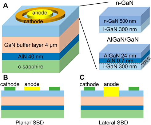
FIGURE 1. (A) Schematic illustrations of n-GaN and AlGaN/GaN SBDs with epitaxial information. The schematic cross-section of (B) planar and (C) lateral SBDs.

TABLE 1. The key material parameters of n-GaN and AlGaN/GaN.
According to the n-GaN and AlGaN/GaN SBDs structures, the characteristics of the energy band and carrier distribution are simulated by Synopsys’ Sentaurus technology computer-aided design (TCAD), and the results are shown in Figure 2. The depletion directions of the planar and lateral SBDs are perpendicular and parallel to the (0,001) plane, respectively. The energy band and carrier distribution are very similar between planar and lateral n-GaN SBDs because both are Ni/n-GaN contacts. The simulation results show that the sample with SBH of about 1.18 eV has a depletion width of about 44.5 nm for n-GaN with doping concentration of 3.4×1017 cm−3, as shown in Figures 2A,B. However, the energy band structures of the planar and lateral AlGaN/GaN SBDs are very different, as shown in Figures 2C,D. The energy band structure of the planar AlGaN/GaN SBD displays that anode metal cannot deplete the 2DEG channel at 0 V, and its SBH is 1.60 eV. The 2DEG is distributed in the i-GaN layer of the AlGaN/GaN heterostructure, which is only a ∼2.8 nm-thick sheet channel. The simulation results of the energy band and carrier distribution of the lateral AlGaN/GaN SBD are shown in Figure 2D. For lateral AlGaN/GaN SBD, the lateral contact of Ni-2DEG can be treated as SBD of a heavily doped n+-GaN sheet channel. The Ni-2DEG forms a SBH of 1.08 eV, which only depletes 4.5 nm 2DEG.
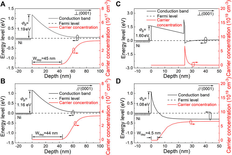
FIGURE 2. The energy band and carrier distribution of (A) planar n-GaN SBD, (B) lateral n-GaN SBD, (C) planar AlGaN/GaN SBD, and (D) lateral AlGaN/GaN SBD at 0 V.
As shown in Figures 3A–H, we measured the I-V and C-V characteristics of each SBD at different temperatures from 298 to 504 K. The I-V and C-V curves conform to traditional SBD depletion characteristics for planar n-GaN SBD, lateral n-GaN SBD, and lateral AlGaN/GaN SBD. However, the I-V and C-V curves of the planar AlGaN/GaN SBD are different from the characteristics of traditional SBD depletion. Because anode metal and 2DEG channel are separated by AlGaN barrier layer. The Von of the planar AlGaN/GaN SBD is as high as 1.64 V since the device conduction requires electrons to pass through the AlGaN barrier layer, while the other three devices show very low Von because electrons only need to overcome the barriers to flow to the anode. The Jr of the planar AlGaN/GaN SBD reaches saturation at pinch-off voltage (-4.2 V) due to 2DEG depletion, as shown in Figure 3C. The capacitance characteristic of planar AlGaN/GaN SBD is fitted to the parallel plate capacitor model of the anode metal and 2DEG [18]. At lower reverse bias voltage, the planar AlGaN/GaN SBD maintains a stable capacitance value due to the characteristics of parallel plate capacitors. With increasing reverse bias voltage, the 2DEG is gradually depleted, which causes the capacitance to drop rapidly due to the disappearance of the plate capacitor. At higher reverse bias voltage, the capacitance tends to zero, the 2DEG is completely depleted, as shown in Figure 3G. The capacitance approaching zero also shows the HR characteristics of the buffer layer. The n-GaN and AlGaN/GaN SBDs of different FP widths are measured, the values of zero bias capacitance are linear with the area of the FP, so the lateral SBD without FP can effectively eliminate the FP capacitance. Compared with the planar SBDs, the capacitances of the lateral SBDs are reduced by two orders of magnitude without sacrificing the performance of the Ron and Jr. This is attributed to two characteristics of lateral SBDs: the small anode area and the elimination of spreading resistance under the anode metal. The capacitances of lateral n-GaN SBD and lateral AlGaN/GaN SBD are 1.35 pF/mm and 0.70 pF/mm, respectively.
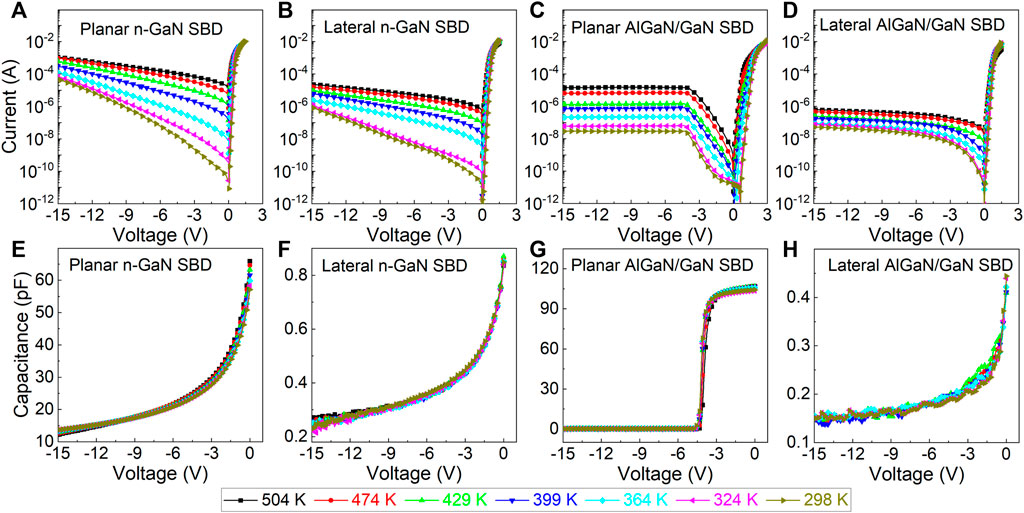
FIGURE 3. The I-V (A–D) and C-V (E–H) characteristics of planar n-GaN SBD, lateral n-GaN SBD, planar AlGaN/GaN SBD, and lateral AlGaN/GaN SBD at temperatures of 504 K, 474 K, 429 K, 399 K, 364 K, 324 K and 298 K.
In order to extract the SBH ΦB, the ideality factor n, and the Ron from the I-V curve, the thermionic emission (TE) can be described as the major forward current contribution [28, 31],
where A is the area of the anode metal, A* is the effective Richardson constant (226.4 Acm−2K−2), k is the Boltzmann constant, and T is the temperature. From the I-V and C-V curves at room temperature, the device parameters of each SBD are summarized in Table 2. The SBHs extracted by the I-V characteristics are lower than the simulation results, which may be due to electron tunneling and inhomogeneity SBHs [27–29]. The ideality factors of each SBD are larger than 1, which indicates that in addition to TE, other transport mechanisms include thermionic field emission (TFE) and field emission (FE) [32, 33]. For planar AlGaN/GaN SBD, the ideality factor of ∼2 illustrates the existence of various transport types other than TE, such as trap-assisted tunneling (TAT) and recombination [34].

TABLE 2. The electrical characteristics of n-GaN SBDs and AlGaN/GaN SBDs at room temperature.
The ideality factors of each SBD are extracted from the I-V curve at different temperatures and shown in Figure 4A, which are larger than 1. Hence, the transport mechanism includes other mechanisms other than TE. What’s more, TE is more sensitive to temperature, and the ideality factors are positively related to 1,000/T due to the domination of the TE mechanism at high temperatures.
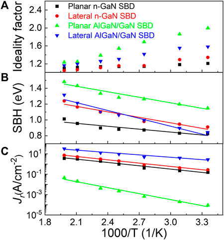
FIGURE 4. (A) Ideality factor, (B) barrier height, and (C) Jr as a dependence of 1,000/T for each SBD device.
Figure 4B shows SBHs for each SBD at temperatures ranging from 298 to 504 K. The SBHs of each SBD were extracted from the forward I-V curves by Eq. 1. The SBHs decrease with increasing 1,000/T due to the inhomogeneous nature of the barrier. The electrons only overcome lower barriers at lower temperatures. With increasing temperature, the energy of the electrons increases to overcome the higher barriers at the Ni/GaN interface, where the higher SBHs were exhibited. The inhomogeneous SBHs can be expressed as a Gaussian distribution with a mean barrier height
In GaN-based SBDs, inhomogeneous SBHs are attributed to multiple factors such as material defects, interface dipole layers, morphological features, and surface Fermi level pinning [27–30, 35]. According to the linear fits of the SBHs vs 1,000/T curve, the values of
At the voltage of -15 V, the Jr vs 1,000/T (Jr-T) characteristics are shown in Figure 4C, which appears linear on the Arrhenius plot. This suggests that the thermal activation mechanism has a dependence on the
The withstand voltage of SBD is a very important parameter for power electronic applications. The reverse breakdown voltages of these SBDs are shown in Figure 5. The planar n-GaN SBD has no breakdown phenomenon at -28.5 V. The lateral n-GaN SBD shows a relatively low leakage current, which is breakdown at -73 V. Compared with n-GaN SBD, the AlGaN/GaN SBDs exhibit a breakdown voltage of more than 2300 V, which is mainly attributed to the undoped AlGaN/GaN materials.
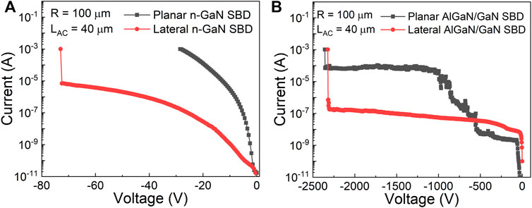
FIGURE 5. Reverse I-V characteristics of (A) n-GaN SBDs and (B) AlGaN/GaN SBDs.
For planar and lateral SBDs, the Ron consists of the RC, channel resistance (Rchannel) and anode resistance (RA). Using the TLM, we calculated the RC and Rchannel for each SBD. Unitized Ron distributions of each SBD are summarized in Figure 6A. The experimental results show that the RA of lateral n-GaN SBD and lateral AlGaN/GaN SBD are 10.5 Ω mm and 9.2 Ω mm, respectively. The RA are much larger than the RC in each SBD, which is probably due to the worsening anode contacts by MIGS. The energy diagram of n-GaN SBD with MIGS is displayed in Figure 6B. The planar AlGaN/GaN SBD exhibits larger RA due to the electrons passing through the AlGaN barrier layer under the anode metal [39].
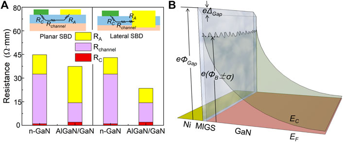
FIGURE 6. (A) Unitized Ron distributions in planar and lateral SBDs. (B) Energy diagram of n-GaN SBD with MIGS and inhomogeneous SBHs.
In summary, the lateral SBDs based on n-GaN and AlGaN/GaN heterostructure were fabricated, and the temperature-dependent I-V and C-V characteristics were used to evaluate the electrical properties, such as transport mechanisms of the forward and reverse current, SBHs, Ron distribution, MIGS, inhomogeneous SBHs, etc. For the planar and lateral n-GaN SBDs, the values of the Von are similar. However, compared with conventional planar AlGaN/GaN SBD, the Von of lateral AlGaN/GaN SBD is reduced from 1.64 V to 0.87 V. The capacitances of lateral n-GaN SBD and lateral AlGaN/GaN SBD are 1.35 pF/mm and 0.70 pF/mm, respectively, which are much smaller than the capacitance of planar SBDs. According to the analysis of inhomogeneous SBHs, etching damage degrades the uniformity of SBHs. Compared with the breakdown voltage of 73 V in the lateral n-GaN SBD, the lateral AlGaN/GaN SBDs exhibit a breakdown voltage of 2322 V. In addition, the RA is much greater than the RC due to worsening anode contact by MIGS from the analysis of the Ron distributions of each SBD.
The raw data supporting the conclusions of this article will be made available by the authors, without undue reservation.
Conceptualization: HL and BZ. Investigation: HL, ZL, FW, YX, XY, and YiL. Methodology: HL and BZ. Project administration: XL, LL, YaL, and ZW. Software: HL and BZ. Validation: HL, ZL, and BZ. Writing—original draft: HL, ZL, and BZ.
This work was supported by Science and Technology Plan of Guangdong Province, China (Grant Nos. 2019B010132003 and 2019B010132001), the joint funding of the Nature Science Foundation of China (NSFC) and the Macao Science and Technology Development Fund (FDCT) of China (Grant No. 62061160368), the National Key Research and Development Program (Grant Nos. 2016YFB0400105 and 2017YFB0403001), and the Zhuhai Key Technology Laboratory of Wide Bandgap Semiconductor Power Electronics, Sun Yat-sen University, China (Grant No. 20167612042080001).
The authors declare that the research was conducted in the absence of any commercial or financial relationships that could be construed as a potential conflict of interest.
All claims expressed in this article are solely those of the authors and do not necessarily represent those of their affiliated organizations, or those of the publisher, the editors and the reviewers. Any product that may be evaluated in this article, or claim that may be made by its manufacturer, is not guaranteed or endorsed by the publisher.
1. Sun Y, Kang X, Zheng Y, Lu J, Tian X, Wei K, et al. Review of the recent progress on GaN-based vertical power Schottky barrier diodes (SBDs). Electronics (2019) 8(5):575. doi:10.3390/electronics8050575
2. Mitova R, Ghosh R, Mhaskar U, Klikic D, Wang M-X, Dentella A. Investigations of 600-V GaN HEMT and GaN diode for power converter applications. IEEE Trans Power Electron (2014) 29(5):2441–52. doi:10.1109/tpel.2013.2286639
3. Zhang L, Liang S, Lv Y, Yang D, Fu X, Song X, et al. High-power 300 GHz solid-state source chain based on GaN doublers. IEEE Electron Device Lett (2021) 42(11):1588–91. doi:10.1109/led.2021.3110781
4. Millan J, Godignon P, Perpina X, Perez-Tomas A, Rebollo J. A survey of wide bandgap power semiconductor devices. IEEE Trans Power Electron (2014) 29(5):2155–63. doi:10.1109/tpel.2013.2268900
5. Vurgaftman I, Meyer JR, Ram-Mohan LR. Band parameters for III-V compound semiconductors and their alloys. J Appl Phys (2001) 89(11):5815–75. doi:10.1063/1.1368156
6. Pearton SJ, Ren F, Zhang AP, Lee KP. Fabrication and performance of GaN electronic devices. Mater Sci Eng R: Rep (2000) 30(3-6):55–212. doi:10.1016/s0927-796x(00)00028-0
7. Ambacher O, Foutz B, Smart J, Shealy JR, Weimann NG, Chu K, et al. Two dimensional electron gases induced by spontaneous and piezoelectric polarization in undoped and doped AlGaN/GaN heterostructures. J Appl Phys (2000) 87(1):334–44. doi:10.1063/1.371866
8. Yu ET, Dang XZ, Asbeck PM, Lau SS, Sullivan GJ. Spontaneous and piezoelectric polarization effects in III-V nitride heterostructures. J Vac Sci Technol B (1999) 17(4):1742–9. doi:10.1116/1.590818
9. Soni A, Shrivastava M. Design guidelines for recessed Schottky barrier AlN/GaN diode for THz applications. IEEE Trans Electron Devices (2021) 68(5):2196–204. doi:10.1109/ted.2021.3064541
10. Shinohara K, Regan DC, Tang Y, Corrion AL, Brown DF, Wong JC, et al. Scaling of GaN HEMTs and Schottky diodes for submillimeter-wave MMIC applications. IEEE Trans Electron Devices (2013) 60(10):2982–96. doi:10.1109/ted.2013.2268160
11. Dang K, Wei K, Hao Y, Zhang J, Zhou H, Huang S, et al. A 5.8-GHz high-power and high-efficiency rectifier circuit with lateral GaN Schottky diode for wireless power transfer. IEEE Trans Power Electron (2020) 35(3):2247–52. doi:10.1109/tpel.2019.2938769
12. Dang K, Zhang J, Zhou H, Yin S, Zhang T, Ning J, et al. Lateral GaN Schottky barrier diode for wireless high-power transfer application with high RF/DC conversion efficiency: From circuit construction and device technologies to system demonstration. IEEE Trans Ind Electron (2020) 67(8):6597–606. doi:10.1109/tie.2019.2939968
13. Zhang T, Zhang J, Zhou H, Zhang Y, Chen T, Zhang K, et al. High-performance lateral GaN Schottky barrier diode on silicon substrate with low turn-on voltage of 0.31 V, high breakdown voltage of 2.65 kV and high-power figure-of-merit of 2.65 GW cm-2. Appl Phys Express (2019) 12(4):046502. doi:10.7567/1882-0786/ab0712
14. Zhang Y, Zhang J, Zhou H, Zhang T, Wang H, Feng Z, et al. Leakage current mechanisms of groove-type tungsten-anode GaN SBDs with ultra low turn-on voltage and low reverse current. Solid State Electron (2020) 169:107807. doi:10.1016/j.sse.2020.107807
15. Li X, Pu T, Li X, Li L, Ao J-P. Correlation between anode area and sensitivity for the TiN/GaN Schottky barrier diode temperature sensor. IEEE Trans Electron Devices (2020) 67(3):1171–5. doi:10.1109/ted.2020.2968358
16. Yao Y, Zhong J, Zheng Y, Yang F, Ni Y, He Z, et al. Current transport mechanism of AlGaN/GaN Schottky barrier diode with fully recessed Schottky anode. Jpn J Appl Phys (2015) 54(1):011001. doi:10.7567/jjap.54.011001
17. Li A, Wang C, He Y, Zheng X, Ma X, Zhao Y, et al. GaN-based super-lattice Schottky barrier diode with low forward voltage of 0.81V. Superlattices Microstruct (2021) 156:106952. doi:10.1016/j.spmi.2021.106952
18. Waller WM, Gajda M, Pandey S, Uren MJ, Kuball M. Lateral charge distribution and recovery of dynamic Ron in AlGaN/GaN HEMTs. IEEE Trans Electron Devices (2018) 65(10):4462–8. doi:10.1109/ted.2018.2865037
19. Yang L, Yao W, Liu Y, Wang L, Dai Y, Liu H, et al. Low capacitance AlGaN/GaN based air-bridge structure planar Schottky diode with a half through-hole. AIP Adv (2020) 10(4):045219. doi:10.1063/5.0004470
20. Lei Y, Lu H, Cao D, Chen D, Zhang R, Zheng Y. Reverse leakage mechanism of Schottky barrier diode fabricated on homoepitaxial GaN. Solid State Electron (2013) 82:63–6. doi:10.1016/j.sse.2013.01.007
21. Yildirim N, Ejderha K, Turut A. On temperature-dependent experimental I-V and C-V data of Ni/n-GaN Schottky contacts. J Appl Phys (2010) 108(11):114506. doi:10.1063/1.3517810
22. Lei W, Nathan MI, Lim TH, Khan MA, Chen Q. High barrier height GaN Schottky diodes: Pt/GaN and Pd/GaN. Appl Phys Lett (1996) 68(9):1267–9. doi:10.1063/1.115948
23. Schmitz AC, Ping AT, Asif Khan M, Chen Q, Yang JW, Adesida I. Schottky barrier properties of various metals on n-type GaN. Semicond Sci Technol (1996) 11(10):1464–7. doi:10.1088/0268-1242/11/10/002
24. Monch W. Barrier heights of real Schottky contacts explained by metal-induced gap states and lateral inhomogeneities. J Vac Sci Technol B (1999) 17(4):1867–76. doi:10.1116/1.590839
25. Tersoff J. Schottky barrier heights and the continuum of gap states. Phys Rev Lett (1984) 52(6):465–8. doi:10.1103/PhysRevLett.52.465
26. Tung RT. The physics and chemistry of the Schottky barrier height. Appl Phys Rev (2014) 1(1). doi:10.1063/1.4858400
27. Shin J-H, Park J, Jang S, Jang T, Kim KS. Metal induced inhomogeneous Schottky barrier height in AlGaN/GaN Schottky diode. Appl Phys Lett (2013) 102(24):243505. doi:10.1063/1.4811756
28. Ren Y, He Z, Dong B, Wang C, Zeng Z, Li Q, et al. Analysis of electrical properties in Ni/GaN Schottky contacts on nonpolar/semipolar GaN free-standing substrates. J Alloys Compd (2022) 898:162817. doi:10.1016/j.jallcom.2021.162817
29. Iucolano F, Roccaforte F, Giannazzo F, Raineri V. Barrier inhomogeneity and electrical properties of Pt/GaN Schottky contacts. J Appl Phys (2007) 102(11):113701. doi:10.1063/1.2817647
30. Werner JH, Guttler HH. Barrier inhomogeneities at Schottky contacts. J Appl Phys (1991) 69(3):1522–33. doi:10.1063/1.347243
31. Wu M, Zheng D-Y, Wang Y, Chen W-W, Zhang K, Ma X-H, et al. Schottky forward current transport mechanisms in AlGaN/GaN HEMTs over a wide temperature range. Chin Phys B (2014) 23(9):097307. doi:10.1088/1674-1056/23/9/097307
32. Benamara Z, Akkal B, Talbi A, Gruzza B. Electrical transport characteristics of Au/n-GaN Schottky diodes. Mater Sci Eng C (2006) 26(2-3):519–22. doi:10.1016/j.msec.2005.10.016
33. Reddy MSP, Kumar AA, Reddy VR. Electrical transport characteristics of Ni/Pd/n-GaN Schottky barrier diodes as a function of temperature. Thin Solid Films (2011) 519(11):3844–50. doi:10.1016/j.tsf.2011.01.258
34. Yan D, Jiao J, Ren J, Yang G, Gu X. Forward current transport mechanisms in Ni/Au-AlGaN/GaN Schottky diodes. J Appl Phys (2013) 114(14):144511. doi:10.1063/1.4824296
35. Roccaforte F, Giannazzo F, Alberti A, Spera M, Cannas M, Cora I, et al. Barrier inhomogeneity in vertical Schottky diodes on free standing gallium nitride. Mater Sci Semicond Process (2019) 94:164–70. doi:10.1016/j.mssp.2019.01.036
36. Shao Z, Chen D, Lu H, Zhang R, Cao D, Luo W, et al. High-gain AlGaN solar-blind avalanche photodiodes. IEEE Electron Device Lett (2014) 35(3):372–4. doi:10.1109/LED.2013.2296658
37. Wen Q, Wang C, Qiu X, Lv Z, Jiang H. Significant performance improvement of AlGaN solar-blind heterojunction phototransistors by using Na2S solution based surface treatment. Appl Surf Sci (2022) 591:153144. doi:10.1016/j.apsusc.2022.153144
38. Zhang H, Miller EJ, Yu ET. Analysis of leakage current mechanisms in Schottky contacts to GaN and Al0.25Ga0.75N/GaN grown by molecular-beam epitaxy. J Appl Phys (2006) 99(2):023703. doi:10.1063/1.2159547
Keywords: GaN, AlGaN/GaN, Schottky barrier diodes, metal-induced gap states, inhomogeneous SBHs
Citation: Liu H, Liang Z, Wang F, Xu Y, Yang X, Liang Y, Li X, Lin L, Wu Z, Liu Y and Zhang B (2022) Analysis of electrical properties in lateral Schottky barrier diode based on n-GaN and AlGaN/GaN heterostructure. Front. Phys. 10:1084214. doi: 10.3389/fphy.2022.1084214
Received: 30 October 2022; Accepted: 11 November 2022;
Published: 21 November 2022.
Edited by:
Ye Yuan, Songshan Lake Material Laboratory, ChinaReviewed by:
Liuan Li, Jilin University, ChinaCopyright © 2022 Liu, Liang, Wang, Xu, Yang, Liang, Li, Lin, Wu, Liu and Zhang. This is an open-access article distributed under the terms of the Creative Commons Attribution License (CC BY). The use, distribution or reproduction in other forums is permitted, provided the original author(s) and the copyright owner(s) are credited and that the original publication in this journal is cited, in accordance with accepted academic practice. No use, distribution or reproduction is permitted which does not comply with these terms.
*Correspondence: Baijun Zhang, emhiYWlqQG1haWwuc3lzdS5lZHUuY24=
Disclaimer: All claims expressed in this article are solely those of the authors and do not necessarily represent those of their affiliated organizations, or those of the publisher, the editors and the reviewers. Any product that may be evaluated in this article or claim that may be made by its manufacturer is not guaranteed or endorsed by the publisher.
Research integrity at Frontiers
Learn more about the work of our research integrity team to safeguard the quality of each article we publish.