
95% of researchers rate our articles as excellent or good
Learn more about the work of our research integrity team to safeguard the quality of each article we publish.
Find out more
ORIGINAL RESEARCH article
Front. Phys. , 14 November 2022
Sec. Optics and Photonics
Volume 10 - 2022 | https://doi.org/10.3389/fphy.2022.1057992
This article is part of the Research Topic State-of-the-Art Laser Spectroscopy and its Applications : Volume II View all 51 articles
 Mei Liu1*†Pengyi Duan1†
 Muhammad Shafi1Wenying Liu1Wenjie Zhang1Can Zhang1Xiaoxuan Hu1Jing Gao2
 Chao Zhang1*
Topological nanomaterials generally exhibit different defect structures, high specific surface areas, and varying bandgaps. These special geometries, energy-level structures, and interfacial interaction properties provide possibilities to explore interesting properties in the surface-enhanced Raman scattering (SERS). Such properties offer unexplored possibilities for exploring interesting physics and materials science in the field of SERS physical property research and further enhancing substrate materials’ SERS activity. In this paper, the ZnSe topological nanowire crystallite structure was grown using the chemical vapor deposition method, twin defects were introduced, and a topological branched structure that caused the corresponding changes in SERS activity was systematically investigated. On topological ZnSe nanowires, rhodamine 6G (R6G), methylene blue (MB), and crystalline violet (CV) molecules were detected using Raman spectroscopy. The Raman signal enhancement of MB on topological branched nanowires was about 1.9 times that of the trunk nanowires. Finally, the national standard measurement of malachite green (MG) content in water bodies were realized. The results suggest that semiconductor ZnSe topographical nanowires are an emerging class of SERS substrates, and a thorough investigation into the relationship between material structure and SERS performance in specific topological regions will provide new evidence for the principle of chemical enhancement of SERS, as well as recommendations for developing precisely functionalized SERS substrate nanomaterials.
Recently, surface-enhanced Raman scattering (SERS) is an accurate and reliable molecular fingerprint technology widely used in biological medicine, environmental monitoring, disease diagnosis, chemical reagent detection and homeland security [1–5]. The scattering enhancement observed in SERS mainly has two mechanisms: electromagnetic (EM) and chemical (CM) enhancement mechanism [6–8]. EM is mainly based on surface plasmon resonance generated by the interaction between the laser source and the SERS active substrate [9, 10]. With the ultra-high SERS enhanced factor up to 1012, noble metal nanomaterials (such as gold, silver, and copper) enhanced via this mechanism enable ultra-sensitive molecular detection [6, 11]. However, because their local surface plasmon resonance covers the majority of visible and near-infrared wavelengths, their selectivity to target molecules is not strong. Meanwhile, the high cost, poor biocompatibility, and poor spectral stability seriously limit their practical applications [12, 13]. The CM-SERS activity mainly comes from the charge transfer (CT) between the substrate and probe molecules. With the development of materials science, various semiconductor materials have been introduced into the research of SERS and CM-SERS has played an important role [14, 15]. The study found that when semiconductor nanomaterials are used as SERS substrates, many parameters such as exciton Bohr radius, band structure, doping type, electron density, chemical stability, stoichiometry, geometric metrology, and crystallinity are controlled. Meanwhile, semiconductor substrates’ spectral stability and repeatability are better than metal substrates.
For semiconductors, doping elements and constructing new structural morphologies can contribute to the improvement of SERS performance [16–18]. One-dimensional nanomaterials exhibit special properties, such as lateral quantum confinement and high specific surface area, resulting in severe uncoordinated surface atoms, providing more active sites for adsorbed molecules. The surface-trapped state of a surface-modified W48O19 nanowire provides an intermediate energy level for charge transfer to further improve the SERS performance of the substrate [19]. A self-assembly superstructured CuO2 with a large number of copper vacancies demonstrates that defect states facilitate the resonant coupling of charge-transfer complexes with incident light and enhance the Raman scattering of target molecules [20]. Constructing the topological structure of one-dimensional materials and studying the SERS performance of topological branches will establish the connection between topological materials and SERS research.
ZnSe is a SERS active semiconductor compound with a bandgap of 2.7 eV at room temperature, which is a kind of short-wave optoelectronic device material with wide application prospects [21–23]. At room temperature, ZnSe is a SERS activity semiconductor compound with a bandgap of 2.7 eV [24]. ZnSe nanomaterials tend to have point defects (such as Zn vacancy, Zn interstitial and Se vacancy) and bulk phase defects (dislocation, stacking faults and twins) when growing in a stoichiometric atmosphere, thus introducing new energy levels. Studies have revealed that the SERS properties of ZnSe nanowires can be changed by the crystal structure and modulation bandgap of ZnSe [25]. The special structural characteristics of ZnSe itself make it easy to produce topological defects at the location where twins are formed in the growth process. These defects promote the formation of more active sites in the secondary topological structure so that the energy level of the whole secondary topological structure changes. It is helpful for studying the SERS properties of topological ZnSe branched nanowires.
Here, we focused on the SERS activity of ZnSe nanowires with a topological branched structure. The relationship between the geometry, defects, electronic energy-level structure, interfacial interaction, and SERS activity of topological ZnSe nanowires was examined. The unique Se vacancy donor defects of the topological branched nanowires provide a proper bandgap for electron–hole separation and good matches with the energy band of the probe molecules. Therefore, the common probe and environmental pollutant molecules have a better enhancement effect on the topological branched nanostructures. On topological branches, the signal of methylene blue (MB) molecules is up to 1.9 times greater than that on the trunk. The results will help us to further investigate the enhancement mechanism of topological semiconductor nanostructures represented by ZnSe in SERS and design and develop some new potent SERS device application platforms.
To prepare Ni-catalyzed ZnSe nanowires, the nickel catalyst (99.99% purity) was deposited on the surface of the substrate with a thickness of about 3 nm using a thermal evaporation method. The ZnSe powder (30 mg, 100 mesh, and 99.99% purity) was deposited in a ceramic boat in the center of the tubular furnace heating zone. Downstream the airflow, SiO2/Si substrates coated with Ni particles were placed 12 cm away from the central source powder as the substrate. In the growth, a high purity argon with a flow rate of 30 standard cubic centimeters per minute (sccm) was used to keep the growth environment close to atmospheric pressure. The pressure was about 96–100 kPa. The growth temperature of ZnSe was 850°C for 1 h, and then the samples were cooled to room temperature naturally.
The SERS activity of topological ZnSe nanowires with various position was measured using the probe molecules: rhodamine 6G (R6G), MB and crystalline violet (CV). In the experiment, R6G, MB, and CV aqueous solutions were prepared with a concentration of 10–5 M. In addition, we configured malachite green (MG) aqueous solution (1 × 10⁻⁶ M to 5 × 10⁻⁴ M) for the practical application of the substrate assay. In SERS measurements, 2 μL of molecule solution with different concentrations was deposited on the fabricated sample surface. The samples were tested after drying in the air for 30 min. For Raman and SERS measurements, some individual nanowires which were not tangled or disjointed with other wires were chosen to obtain the signal.
The Zeiss Sigma 500 scanning electron microscope (SEM, Sigma 500, Zeiss, Germany) was equipped with an energy-dispersive spectrometer (EDS) to investigate the microstructure. Using an X-ray diffractometer (XRD, Ultima, Rigaku, Japan) with voltage: 40 kV, current: 40 mA, scan step: 0.02°, scan speed: 4°/min, and scan range: 10–60°, the crystal structure of topologically branched ZnSe nanowires was detected. The structure of the topological ZnSe nanowires was characterized using high-resolution transmission electron microscopy (HRTEM, JEM-2100, JEOL Ltd., Japan) with an accelerating voltage of 200 kV. All Raman spectra and photoluminescence (PL) were measured using an HR Evolution instrument produced by HORIBA Scientific, equipped with a 532 nm (Raman and SERS) and 325 nm (PL) laser. The spectrometer grating of 600 g/mm, the laser spot diameter of 2 μm, and the signal acquisition time of 4 s were chosen. A ×50 objective lens and a laser excitation energy of 48 mW and 12 mW were used for Raman and SERS measurements, respectively. A ×40 objective lens and a laser excitation energy of 6.25 mW were used for PL measurements. The resulting spectra are the average of the spectral signal intensity obtained from 20 locations in the same sample. All the measurements were performed at room temperature.
Figure 1 shows a schematic diagram of the preparation of topological branched nanowires and the probe molecular detection. Figure 2 shows the SEM and EDS images of a topological grading tree-like structure of ZnSe nanowires. The diameters of the secondary branch (marked as B) and trunk (marked as T) are about 300 nm and 1200 nm, respectively. The branch is narrower than the trunk. Most of the branch nanowires are concentrated on the surface of the substrate. A crystal ball can be seen at the tip of the nanowires. The EDS results showed that the tip of the nanowires has little Zn element, but the dominant elements are Se and Ni. ZnSe topological nanostructures are grown by a vapor–liquid–solid (VLS) mechanism. The nanowire compositions are ZnSe with no detectable traces of other elements, except for the weak C and O signals originating from the substrate. The component proportion of the trunk and the topological branch differed under the same conditions. In the trunk, the atomic ratio of Zn and Se is closer to the stoichiometric ratio. The component ratio of Zn and Se is different along the growth direction of the topological branch and Se is a lesser element.

FIGURE 1. Diagram of the preparation of a ZnSe topological branched nanowire SERS substrate and the detection of SERS performance.
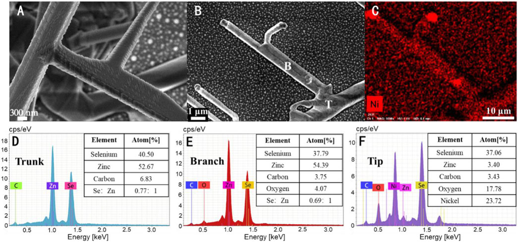
FIGURE 2. (A) SEM image of topological ZnSe nanowires. (C) EDS mapping scan of the image (B). (D–F) Spectra of EDS scanning on the trunk, topological branch, and top of nanowires, respectively. The table in the upper right corner of each image corresponds to the elements and their proportions in each test position.
XRD further characterized the crystal structure of the ZnSe nanowires as shown in Figure 3A. The strong signal at 2
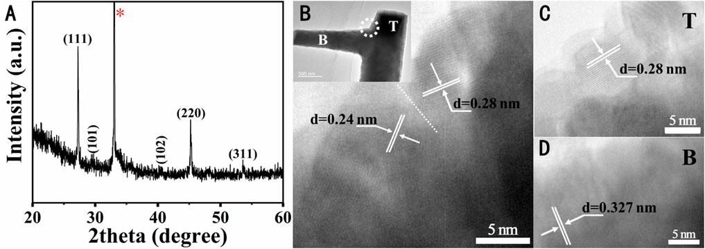
FIGURE 3. (A) XRD spectra of ZnSe nanowires, labeled with diffraction plane of the zinc blende-, wurtzite-ZnSe crystal structure. (B) HRTEM of the junction of the trunk and topological branch of the topological branched nanowires, and the inset in the upper left corner shows the full view of this position. HRTEM of the (C) trunk and (D) topological branched nanowires.
Under the low dissolution temperature, Se ions are evaporated firstly from the source powder during the growth process. The Se atoms were transported from the evaporation source to the growth zone downstream and combined with the Ni nanoparticles on the substrate to form a Ni-Se solid solution alloy, which plays a nucleation role in the growth of ZnSe nanowires. The Zn ions are combined with the Se-Ni solid solution. When the number of these atoms exceeds the equilibrium concentration in the liquid phase, the crystallized ZnSe nanowires precipitate underneath the alloy droplet, while the alloy remains at the tip of the nanowires. At the initial stage of nanowire growth, sufficient source powder can make nanowires with fewer Se defects. The topological branched nanowires precipitate at the side of the trunk, as shown in Figure 2A. During the growth of ZnSe nanowires, the atomic binding energy varies with pressure and temperature, resulting in defects. Ni particles not involved in the nucleation initiation stage can move on the substrate surface at a certain temperature. The Ni catalyst will be absorbed in the defects of the first-formed ZnSe nanowires, which will lower the surface energy and result in the sprouting of subnanowires from the defects and the formation of secondary topological nanostructures.
Furthermore, the Ni droplets remaining at the trunk defects are smaller than the clustered droplets on the SiO2/Si substrate. Hence, the diameter of the grown topological branched nanowires is narrower. Simultaneously, a large amount of Se was consumed with the extension of growth time, and the Ni particles of the grown catalysts melted and mixed with Zn and Se. Se element of the topological branch is less than that of the trunk. In addition, some Se atoms still were re-evaporated in the deposition, so the amount of Se element is less than that of Zn both in trunks and branches. Based on the VLS growth mode, the V, L, and S phases are closely coupled, and changes in the gas phase may affect the solid phase. It is difficult to obtain complete stoichiometry of ZnSe and many other II-VI semiconductors [26].
Figure 4A shows the Raman peaks of the trunk and the topological branches of the ZnSe nanowires, respectively. Raman peaks at 205 cm−1 and 252 cm−1 can be found in the trunk and topological branches, which are corresponding to the scattering of transverse optical (
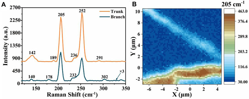
FIGURE 4. (A) Raman spectra of ZnSe nanowires (the ordinate of topological branches is ×3 times for the result) and (B) corresponding mapping at 205 cm−1.
Figure 5 shows the PL spectra of the trunk, and the topological branched nanostructures of ZnSe measured in the wavelength range of 300–700 nm to investigate the optical properties of ZnSe nanostructures. The PL spectra of both the trunk and topological branched nanowires consist of three emission bands: a peak at about 380 nm, a narrow half-width ratio near-band edge (BE) peak at 460–470 nm, and a broad half-width ratio deep-defect (DD) band at 500–750 nm. In the trunk, the peak at 378 nm (3.28 eV) is the exciton emission peak generated by the direct recombination of electron–hole pairs, and the peak at 462 nm (2.68 eV) belongs to the intrinsic peak of ZnSe material. The DD broad emission band of the trunk can be divided into two peaks centered at 566 nm (T1) and 654 nm (T2) by fitting a Gaussian function. The emission at 566 nm is attributed to deep-defect-related emission, ascribed to the recombination of a donor–acceptor pair involving Zn vacancies and interstitials and surface emission [32–34]. A single local level mainly determines the characteristic peak at 654 nm (1.89 eV) to confirm that the recombination emission peak is caused by the direct transition of the Zn interstitial electron donor to the valence band and the higher emission intensity is caused by the higher Zni concentration excited by more Se ions [35]. The DD peaks on the topological branches can be fitted to three sub-bands centered at 512 nm (B1), 576 nm (B2), and 626 nm (B3) by the Gaussian function in the PL spectra for topological branches, and the peaks at 381 nm, 471 nm, and 576 nm are similar to the trunk. The emission peak at 512 nm (2.43 eV), which is different from the trunk peak, is derived from the surface trap state. The emission wavelength is caused by the conduction band (CB) to the single negatively charged Zn-vacancy (VZn−) due to the high surface volume ratio [36]. Another unique PL peak at 626 nm (1.98 eV) of the topological branches corresponds to a donor–acceptor pair, charged Zn-vacancy (VZn−) from VSe.
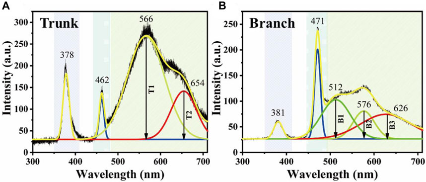
FIGURE 5. PL spectrum of ZnSe nanowires with the (A) trunk and (B) the topological branch.
According to the PL spectra of ZnSe nanowires, BE emission peak intensity on the trunk is weaker than DD emission peak intensity. In contrast, BE peak intensity on the topological branches is stronger than DD peak intensity. This is related to the growth conditions. The growth may introduce inherent point defect Zn interstitial when the Se content is rich in the early growth stage, which may cause the strong DD emission in the trunk. The lower concentration of Zn vacancy leads to the lower intensity of the DD emission peak on the topological branches when the nanowires grow under zinc-rich conditions at the later growth stage due to the lower melting point of Se in the source powder, longer growth time and higher Se activity [33]. According to the aforementioned evidence, there are emission peaks caused by different structural defects in the PL spectra of the trunk and topological branches. Therefore, different defect levels generated by the two have different effects on charge transfer, which may affect SERS results.
R6G and CV have a large Raman scattering cross section. The absorption peak of R6G is near 532 nm [37]. The excitation wavelength in the absorption region will lead to molecular resonance and cause a strong resonance Raman effect [38]. The maximum absorption wavelengths of CV and MB are 590 nm and 664 nm, respectively, and there is no resonance Raman effect under 532 nm excitation light [39]. CV is a cationic industrial dye with a complex structure and hard degradation [40]. It is widely used in the area of aquaculture disease prevention and control. MB is often used to localize sentinel lymph nodes in medical and prevent black spot disease for fish in aquaculture [41]. However, R6G, CV and MB dyes pose a hazard to the environment and animals, plants and human health [42]. Focusing on the SERS activity of the topological structure of ZnSe nanowires on these three dye molecules can help us study the topological structure’s effect on the SERS activity and analyze the generality of the SERS activity based on topological nanowires of different chemical molecules. The SERS results of MB, CV and R6G molecules shown in Figure 6 indicate that the enhanced Raman signals of MB, CV and R6G absorbed on the topological branches are better than those absorbed on the trunks of ZnSe nanowires. Among them, the Raman peak intensity of the MB molecules at 1625 cm−1 is about 1.9 times higher than that of the trunk, and the peak of the CV molecules at 1622 cm−1 is about 3.2 times higher than that of the trunk. The relative intensity of the 1651 cm−1 peaks of R6G molecules on the topological branches reached 1.5 times higher than that on the trunk. For the Raman enhancement of R6G molecule, the contribution of resonance excitation is much greater than that of charge transfer. Therefore, the differences in the relative peak intensities of R6G molecules on the trunk and branches are the smallest among the three probe molecules.
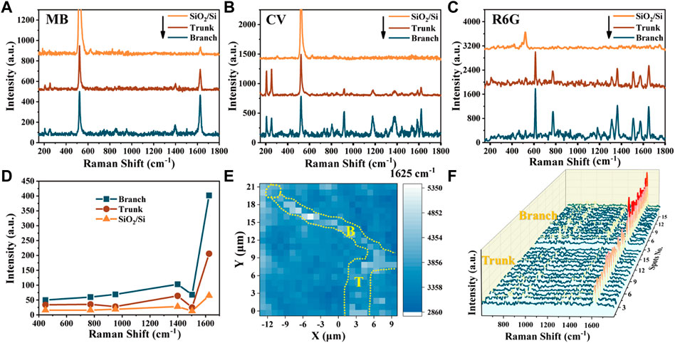
FIGURE 6. Raman spectra of (A) MB, (B) CV, and (C) R6G deposited on trunks and topological branches of ZnSe nanowire substrates; all concentration is 10−5 M. (D) Intensities of the peaks of MB (10−5 M) deposited on the trunks, topological branches, and blank SiO2/Si substrate. (E) Spatial mapping of the SERS intensity at 1625 cm−1 of MB probe molecules on ZnSe SERS substrates over an area larger than 21 μm × 21 μm. (F) SERS peak values of MB (10–5 M) were taken from 15 random positions on the trunk and branch of the topological nanowire SERS substrate.
The SERS signals of different peaks of MB molecules with a concentration of 10–5 M were further analyzed to obtain the different enhancement mechanisms of the trunk and topological branches of ZnSe nanowires. The weak peaks at 448, 772, 951, and 1502 cm−1 of MB molecules correspond to skeletal deformation of C-N-C, in-plane bending of C-H, in-plane bending of C-H, and asymmetrical stretching of C-C, respectively. Two prominent peaks at 1397 cm−1 and 1625 cm−1 are attributed to symmetrical stretching of C-N and ring stretching of the C–C vibration mode, respectively [43]. The intensities of Raman peaks of MB on the different positions of ZnSe nanowires were compared to those on the empty substrate and are shown in Figure 6D. The enhancement of the peak at 1625 cm−1 is the largest. The different enhancement of different vibration modes inhibits some surface molecular vibration due to the coupling binding effect of substrate and probe molecules [44, 45].
Figure 6E shows that the mapping scans of the peak at 1625 cm−1 of MB (concentration of 10–5 M) adsorbed on different positions of ZnSe nanowires. At the tip of the nanowires, there is almost no enhancement of the signal of the MB molecule, which indicates that the catalyst nickel metal particles do not contribute to the enhancement of the Raman signal of the probe molecule. The areas and boundaries of the enhancement of the Raman signal exhibited a higher relative peak intensity around the topological branched nanowires than around the trunk nanowires. The relative peak intensities in the SERS mapping of MB molecules on the topological branches and trunks are opposite to the results presented in the Raman mapping of the sample. We collected 15 points arbitrarily at different locations on the substrate as SERS spectra of MB, as shown in Figure 6F. It can be observed that the average peak intensity on the branch is higher than that on the trunk, indicating that the topological nanowires on the SERS substrate have high repeatability.
It is generally known that chemical enhancement consists of three main contributions: 1) molecular resonance due to laser excitation; 2) Raman enhancement due to electrostatic charge transfer caused by the substrate–molecule interaction; and 3) charge transfer resonance between the molecule and substrate. Figure 7 shows the energy levels of CB, VB, and defect states of ZnSe and the highest occupied molecular orbital (HOMO) and the lowest unoccupied molecular orbital (LUMO) of MB molecules. This plot is based on the PL spectrum of the topological branched nanowires [46]. When the photon energy is high enough, electrons are excited from the VB of the substrate to higher energy levels in the CB of the substrate coupled to the molecular energy levels above LUMO during charge transfer between ZnSe nanostructures and MB-adsorbed molecules. These excited state electrons (except those leaping to the valence band to be recombined) are transferred to the molecular energy levels above LUMO via vibrational coupling of the energy levels, causing the molecular polarization tensor to amplify, giving rise to the SERS effect or electrons are excited from the HOMO of the molecule to higher levels of the LUMO of the molecule that are coupled to the energy levels above the substrate conduction band and transferred to the CB by vibrational coupling. New defect energy levels are also introduced by a defect during growth. The relative energy of the Se vacancy energy level to the VB of ZnSe is about 2.24 eV, very close to the energy of the excitation light (2.3 eV) since there are more Se vacancy donor defects on the topological branches than on the trunk. After absorbing the incident light energy, the electrons on the branch valence band are more easily excited to the defect level and then jump to the coupling level above the CB level and then inject into the LUMO of MB through vibration coupling so that the polarization tensor of the MB probe molecule becomes larger, and the SERS signal becomes stronger. Moreover, the special structural properties of ZnSe itself make it easy to produce topological structure defects at the sites where twinning occurs during the growth of nanowires. The generation of these defects induces more active sites in the secondary topological dendritic structure, which causes energy-level changes in the entire secondary topology and facilitates the further enhancement of the SERS activity.
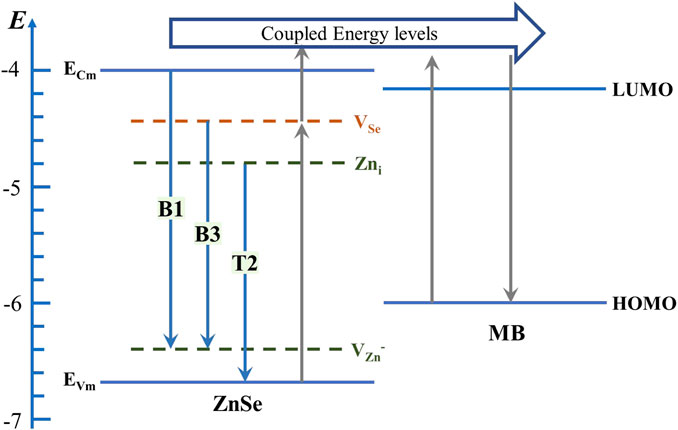
FIGURE 7. Energy-level diagram presenting the SERS ability mechanism on ZnSe microstructures using methylene blue. Abbreviation: VZn− = monoionized zinc vacancy defect; Zni = zinc interstitial monodionized donor defect; VSe = monoionized selenium vacancy defect.
To present the practical application of this SERS active substrate, MG were tested. MG is an ingredient contained in the “potent drug” used in aquaculture to fight against water mold disease in fish and water mold disease in fish eggs, which can be carcinogenic when used in excessive amounts for a long time and is prohibited in the field of pollution-free aquaculture. Figures 8A,B show the concentration gradient detection of MG by the branch and trunk as active substrates, respectively. The branch showed a better detection performance with a limit of detection of 5 × 10⁻⁶ M (the limit of detection of the trunk was 1 × 10⁻⁵ M). Both were lower than the newly revised national use standard of 6.85 × 10⁻⁵ M in the Food Safety Law. Figure 8C shows the detection at the trunk and branch of the topological ZnSe nanowires and the obvious linear relationship between the concentration of MG and the peak intensity at 1616 cm−1, and the R2 values of the trunk and branch are above 0.93, showing good SERS performance and quantitative detection results.

FIGURE 8. (A,B) Raman peaks in the range of 5 × 10⁻⁴ M–10–6 M for MG concentration on the branch and trunk of the ZnSe topological branched SERS substrate, respectively. (C) SERS spectra at 1616 cm−1 on trunk and branch substrates versus different MG concentrations on a logarithmic scale.
In conclusion, physical vapor deposition prepared topological ZnSe nanostructures on silicon substrates. The growth mechanism for the formation of such topological branched structures is discussed. The defects caused by the different structures developed independently are characterized. It is also examined that it leads to different enhancement effects when used as an SERS active substrate. It is shown that the formation of topological nanostructures of ZnSe nanowires in the absence of metal addition enhances surface Raman scattering in which the Se vacancy donor defects in the branches have a prominent contribution to SERS. The nanobranched active ZnSe substrates were identified better than nanotrunks when the enhancement was tested with several probe molecules. In the detection of toxic substances, MG reflected good quantitative detection results, the detection limit of MG reached 5 × 10⁻⁶ M. Studying the SERS activity of ZnSe topological nanostructures offer suggestions for using semiconductors in optoelectronic materials and active substrates to improve molecular detection and show great potential applications in different fields.
The original contributions presented in the study are included in the article/Supplementary Material; further inquiries can be directed to the corresponding authors.
PD: investigation and writing—original draft preparation. MS: methodology. WL and WZ: data curation. CZ and XH: software. JG: search, collect and synthesize the related literatures. ML and CZ: project administration and funding acquisition.
All the authors were grateful for financial assistance from the National Natural Science Foundation of China (NSFC), under Grant Nos. 12074229 and 12174229.
The authors declare that the research was conducted in the absence of any commercial or financial relationships that could be construed as a potential conflict of interest.
All claims expressed in this article are solely those of the authors and do not necessarily represent those of their affiliated organizations, or those of the publisher, the editors, and the reviewers. Any product that may be evaluated in this article, or claim that may be made by its manufacturer, is not guaranteed or endorsed by the publisher.
1. Bharati M. S., Soma V. R. Flexible SERS substrates for hazardous materials detection: Recent advances. Opto-electron Adv (2021) 4:210048–8. doi:10.29026/oea.2021.210048
2. Ji C., Lu J., Shan B., Li F., Zhao X., Yu J.,. The origin of Mo2C films for surface-enhanced Raman scattering analysis: Electromagnetic or chemical enhancement? J Phys Chem Lett (2022) 13:8864–71. doi:10.1021/acs.jpclett.2c02392
3. Zhao Y. Y., Ren X. L., Zheng M. L., Jin F., Liu J., Dong X. Z.,. Plasmon-enhanced nanosoldering of silver nanoparticles for high-conductive nanowires electrodes. Opto-electron Adv (2021) 4:200101–1. doi:10.29026/oea.2021.200101
4. Hao Q., Huang H., Fan X., Yin Y., Wang J., Li W.,. Controlled patterning of plasmonic dimers by using an ultrathin nanoporous Alumina membrane as a shadow mask. ACS Appl Mater Inter (2017) 9:36199–205. doi:10.1021/acsami.7b11428
5. Zhang C., Li Z., Qiu S., Lu W., Shao M., Ji C.,. Highly ordered arrays of hat-shaped hierarchical nanostructures with different curvatures for sensitive SERS and plasmon-driven catalysis. Nanophotonics (2021) 11:33–44. doi:10.1515/nanoph-2021-0476
6. Shafi M., Liu R., Zha Z., Li C., Du X., Wali S.,. Highly efficient SERS substrates with different Ag interparticle nanogaps based on hyperbolic metamaterials. Appl Surf Sci (2021) 555:149729. doi:10.1016/j.apsusc.2021.149729
7. Otto A. The ‘chemical’ (electronic) contribution to surface-enhanced Raman scattering. J Raman Spectrosc (2005) 36:497–509. doi:10.1002/jrs.1355
8. Zha Z., Liu R., Gao J., Yang W., Shafi M., Liu C.,. Graphene-covered Silver nanoisland array coupling with hyperbolic metamaterials for SERS sensing. ACS Appl Nano Mater (2022) 5:6618–26. doi:10.1021/acsanm.2c00665
9. Tian Z. Q., Ren B., Wu D. Y. Surface-enhanced Raman scattering: From noble to transition metals and from rough surfaces to ordered nanostructures. J Phys Chem B (2002) 106:9463–83. doi:10.1021/jp0257449
10. Guo L., Cao H., Cao L., Yang Y., Wang M., SERS study of wheat leaves substrates with two different structures. Opt Commun (2022) 510:127921. doi:10.1016/j.optcom.2022.127921
11. Dieringer J. A., Wustholz K. L., Masiello D. J., Camden J. P., Kleinman S. L., Schatz G. C., Surface-enhanced Raman excitation spectroscopy of a single rhodamine 6G molecule. J Am Chem Soc (2009) 131:849–54. doi:10.1021/ja8080154
12. Fu Y., Cao J., Yamanouchi K., Xu H. Air-laser-based standoff coherent Raman spectrometer. Ultrafast Sci (2022) 2022:9867028–9. doi:10.34133/2022/9867028
13. Zhang Z., Zhang F., Xu B., Xie H., Fu B., Lu X.,. High-sensitivity gas detection with air-lasing-assisted coherent Raman spectroscopy. Ultrafast Sci (2022) 2022:1–8. doi:10.34133/2022/9761458
14. Zhang Y., Shi Y., Wu M., Zhang K., Man B., Liu M. Synthesis and surface-enhanced Raman scattering of ultrathin SnSe(2) nanoflakes by chemical vapor deposition. Nanomaterials (Basel) (2018) 8:8070515. doi:10.3390/nano8070515
15. Liu M., Shi Y., Wu M., Tian Y., Wei H., Sun Q.,. UV surface-enhanced Raman scattering properties of SnSe2 nanoflakes. J Raman Spectrosc (2020) 51:750–5. doi:10.1002/jrs.5846
16. Zheng Z., Cong S., Gong W., Xuan J., Li G., Lu W., et al. Semiconductor SERS enhancement enabled by oxygen incorporation. Nat Commun (2017) 8:1993. doi:10.1038/s41467-017-02166-z
17. Lombardi J. R., Birke R. L., Theory of surface-enhanced Raman scattering in semiconductors. J Phys Chem C (2014) 118:11120. doi:10.1021/jp5020675
18. Yang L., Peng Y., Yang Y., Liu J., Huang H., Yu B., et al. A novel ultra-sensitive semiconductor SERS substrate boosted by the coupled resonance effect. Adv Sci (Weinh) (2019) 6:1900310. doi:10.1002/advs.201900310
19. Gu L. J., Ma C. L., Zhang X. H., Zhang W., Cong S., Zhao Z. G. Populating surface-trapped electrons towards SERS enhancement of W18O49 nanowires. Chem Commun (Camb) (2018) 54:6332–5. doi:10.1039/c8cc03880e
20. Lin J., Shang Y., Li X., Yu J., Wang X., Guo L. Ultrasensitive SERS detection by defect engineering on single Cu2O superstructure particle. Adv Mater (2017) 29:1604797. doi:10.1002/adma.201604797
21. Qiao S., Sampaolo A., Patimisco P., Spagnolo V., Ma Y. Ultra-highly sensitive HCl-LITES sensor based on a low-frequency quartz tuning fork and a fiber-coupled multi-pass cell. Photoacoustics (2022) 27:100381. doi:10.1016/j.pacs.2022.100381
22. Liu X., Ma Y. Tunable diode laser absorption spectroscopy based temperature measurement with a single diode laser near 1.4 μm. Sensors (Basel) (2022) 22:166095. doi:10.3390/s22166095
23. Ma Y., Lewicki R., Razeghi M., Tittel F. K., QEPAS based ppb-level detection of CO and N2O using a high power CW DFB-QCL. Opt Express (2013) 21:1008–19. doi:10.1364/OE.21.001008
24. Zhang Q., Li H., Ma Y., Zhai T. ZnSe nanostructures: Synthesis, properties and applications. Prog Mater Sci (2016) 83:472–535. doi:10.1016/j.pmatsci.2016.07.005
25. Wang G., Wei H., Tian Y., Wu M., Sun Q., Peng Z.,. Twin-ZnSe nanowires as surface enhanced Raman scattering substrate with significant enhancement factor upon defect. Opt Express (2020) 28:18843–58. doi:10.1364/OE.388439
26. Zhang X. T., Liu Z., Ip K. M., Leung Y. P., Li Q., Hark S. K. Luminescence of ZnSe nanowires grown by metalorganic vapor phase deposition under different pressures. J Appl Phys (2004) 95:5752–5. doi:10.1063/1.1699497
27. Shan C. X., Liu Z., Zhang X. T., Wong C. C., Hark S. K. Wurtzite ZnSe nanowires: Growth, photoluminescence, and single-wire Raman properties. Nanotechnology (2006) 17:5561–4. doi:10.1088/0957-4484/17/22/006
28. Wu H., Dittmer J. J., Alivisatos A. P. Hybrid nanorod-polymer solar cells. Science (2002) 295:2425–7. doi:10.1126/science.1069156
29. Irmer G., Monaico E., Tiginyanu I. M., Gärtner G., Ursaki V. V., Kolibaba G. V.,. Fröhlich vibrational modes in porous ZnSe studied by Raman scattering and Fourier transform infrared reflectance. J Phys D: Appl Phys (2009) 42:045405. doi:10.1088/0022-3727/42/4/045405
30. Irwin J. C., LaCombe J. Second-order Raman spectrum of ZnSe. Can J Phys (1970) 48:2499–506. doi:10.1139/p70-314
31. Monaico E., Ursaki V. V., Tiginyanu I. M., Dashevsky Z., Kasiyan V., Boyd R. W. Porosity-induced blueshift of photoluminescence in CdSe. J Appl Phys (2006) 100:053517. doi:10.1063/1.2338833
32. Geng B. Y., Du Q. B., Liu X. W., Ma J. Z., Wei X. W., Zhang L. D. One-step synthesis and enhanced blue emission of carbon-encapsulated single-crystalline ZnSe nanoparticles. Appl Phys Lett (2006) 89:033115. doi:10.1063/1.2227964
33. Philipose U., Xu T., Yang S., Sun P., Ruda H. E., Wang Y. Q.,. Enhancement of band edge luminescence in ZnSe nanowires. J Appl Phys (2006) 100:084316. doi:10.1063/1.2362930
34. Geng J., Liu B., Xu L., Hu F. N., Zhu J. J. Facile route to Zn-based II-VI semiconductor spheres, hollow spheres, and core/shell nanocrystals and their optical properties. Langmuir (2007) 23:10286–93. doi:10.1021/la701299w
35. Makhnii V. P., Tkachenko I. V. Mechanism for forming the red emission band of ZnSe<Te> scintillation crystals. J Opt Technol (2003) 70:665–8. doi:10.1364/jot.70.000665
36. Masalov A. A., Seminko V. V., Kononets N. V., Maksimchuk P. O., Bespalova , Voloshina L. I.,. ZnSe nanocrystals obtained in pores of SiO2 matrix with temperature stable green luminescence. J Lumin (2017) 181:337–44. doi:10.1016/j.jlumin.2016.09.043
37. Vogel R., Meredith P., Harvey M. D., Rubinsztein-Dunlop H. Absorption and fluorescence spectroscopy of rhodamine 6G in titanium dioxide nanocomposites. Spectrochimica Acta A: Mol Biomol Spectrosc (2004) 60:245–9. doi:10.1016/s1386-1425(03)00218-x
38. Wu H., Wang H., Li G. Metal oxide semiconductor SERS-active substrates by defect engineering. Analyst (2017) 142:326–35. doi:10.1039/c6an01959e
39. Deneme I., Liman G., Can A., Demirel G., Usta H., Enabling three-dimensional porous architectures via carbonyl functionalization and molecular-specific organic-SERS platforms. Nat Commun (2021) 12:6119. doi:10.1038/s41467-021-26385-7
40. Cañamares M. V., Chenal C., Birke R. L., Lombardi J. R., DFT, SERS, and single-molecule SERS of crystal violet. J Phys Chem C (2008) 112:20295–300. doi:10.1021/jp807807j
41. Fengzhang T., Huimei Y., Zhuguang L., Lanlan C., Liang Z. Study on adsorption properties and mechanism of methylene blue on coal fly ash by spectrophotometry. Chin J Spectrosc Lab (2010) 27:1116–21. doi:10.1145/1722024.1722072
42. Shanmugam S., Ulaganathan P., Sivasubramanian S., Esakkimuthu S., Krishnaswamy S., Subramaniam S. Trichoderma asperellum laccase mediated crystal violet degradation-Optimization of experimental conditions and characterization, Journal of Environmental Chemical Engineering 5 (2017). p. 222–31. doi:10.1016/j.ibiod.2017.08.001
43. Li C., Huang Y., Lai K., Rasco B. A., Fan Y. Analysis of trace methylene blue in fish muscles using ultra-sensitive surface-enhanced Raman spectroscopy. Food Control (2016) 65:99–105. doi:10.1016/j.foodcont.2016.01.017
44. Creighton J. A. Surface Raman electromagnetic enhancement factors for molecules at the surface of small isolated metal spheres: The determination of adsorbate orientation from sers relative intensities. Surf Sci (1983) 124:209–19. doi:10.1016/0039-6028(83)90345-x
45. Moskovits M., Suh J. S. Surface geometry change in 2-naphthoic acid adsorbed on silver. J Phys Chem (2002) 92:6327–9. doi:10.1021/j100333a030
Keywords: surface-enhanced Raman scattering, growth defect nanowires, topological nanostructure, energy-level matching, charge transfer
Citation: Liu M, Duan P, Shafi M, Liu W, Zhang W, Zhang C, Hu X, Gao J and Zhang C (2022) Surface-enhanced Raman spectroscopic activity study on topological ZnSe nanostructures. Front. Phys. 10:1057992. doi: 10.3389/fphy.2022.1057992
Received: 30 September 2022; Accepted: 17 October 2022;
Published: 14 November 2022.
Edited by:
Yufei Ma, Harbin Institute of Technology, ChinaReviewed by:
Jun Dong, Xi’an University of Posts and Telecommunications, ChinaCopyright © 2022 Liu, Duan, Shafi, Liu, Zhang, Zhang, Hu, Gao and Zhang. This is an open-access article distributed under the terms of the Creative Commons Attribution License (CC BY). The use, distribution or reproduction in other forums is permitted, provided the original author(s) and the copyright owner(s) are credited and that the original publication in this journal is cited, in accordance with accepted academic practice. No use, distribution or reproduction is permitted which does not comply with these terms.
*Correspondence: Mei Liu, bGl1bWVpQHNkbnUuZWR1LmNu; Chao Zhang, Y3pzZG51QDEyNi5jb20=
†These authors have contributed equally to this work
Disclaimer: All claims expressed in this article are solely those of the authors and do not necessarily represent those of their affiliated organizations, or those of the publisher, the editors and the reviewers. Any product that may be evaluated in this article or claim that may be made by its manufacturer is not guaranteed or endorsed by the publisher.
Research integrity at Frontiers
Learn more about the work of our research integrity team to safeguard the quality of each article we publish.