- 1Institute of Semiconductors, Guangdong Academy of Sciences Guangzhou
Guangzhou China - 2Songshan Lake Materials Laboratory, Songshan Lake Innovation and Entrepreneurship Community City A1, Dongguan, China
We report the Cl-based inductively coupled plasma etching of N-polar Al(Ga)N layers obtained from layer transfer. It is found that debris appeared on the etched N-polar surface after exposing in air for a short period whereas the etched Al-/Ga-polar surface was clean and smooth. The debris can be completely self-vanished on the N-polar Al0.4Ga0.6N surface after exposing in air for a few hours but still remained on the N-polar GaN surface even after over 1 month. The surface chemical analysis results suggested that the debris is the result of Cl-related byproduct generated during the etching process. Byproducts like Al(Ga)Clx and its derivatives are believed to cover on the N-polar surface after the inductively coupled plasma etching and increase the etched surface roughness significantly. The formation and disappearance of debris are attributed to the formation of Al(Ga)Clx⋅ 6H2O crystals when Al(Ga)Clx absorbs moisture in the air and its spontaneous decomposition on the N-polar surface, respectively. Adding O2/SF6 in the process helps remove Al(Ga)Clx byproducts but at the cost of roughened surface/reduced etch rate. With an additional cleaning process after etching, an uniform and smooth N-polar GaN surface with a low root-mean-square surface roughness of 0.5–0.6 nm has been successfully obtained at a reasonable etch rate (∼150 nm/min). The results can provide valuable guidance for the fabrication of high-performance N-polar GaN devices.
Introduction
Crystal polarity is a very important feature of wurtzite GaN material. GaN exhibits two different atomic sequences along the opposite directions of the crystal axis. GaN growing along the direction [0001] is Ga-polar and growing along the direction of [0001] is N-polar [1]. Different polarity materials show different properties, so the related devices’ performance will be different. High electron mobility transistors (HEMTs) based on N-polar GaN/AlGaN hetero-structures possess some intrinsic advantages [2–4] due to the opposite polarity to the conventional Ga-polar HEMT devices, such as low contact resistance [5, 6], strong AlGaN back barrier [7], and flexibility in device scaling [8]. High performance N-polar HEMT devices epitaxial grown directly on c-plane sapphire [9] or C-face SiC [10] substrates have already been demonstrated. However, the growth of device-level high quality N-polar nitride materials is rather challenging which requires a much higher growth temperature [10], relatively low V/III ratio [11], and miscut substrates [12] in order to suppress oxygen impurity incorporation and surface hillocks. Alternative approach is to fabricate devices on the backside of a Ga-polar thin film through substrate removal [13] and layer transfer [14, 15]. This method can provide high crystalline N-polar materials and enables the possibility of fabricating N-polar devices on large scale Si substrates, promising for low-cost and mass production. In such a process, an etching of the buffer layers from the N-face side is required after substrate removal in order to expose the N-polar GaN/AlGaN channel layer [16]. On Si substrates, the buffer layers are usually micrometer-thick consisting of multiple Al(Ga)N/GaN layers, such as step-graded AlGaN layers and AlN/GaN super lattices [17]. A uniformly smooth etching surface is particularly important for subsequent device fabrication [18]. For instance, if the etching surface is of high roughness, the resulting GaN channel layer thickness would be of high non-uniformity, which will ultimately impact the on-resistance of HEMT devices.
Wet etching in hot alkaline solutions such as potassium hydroxide [19] and dry etching in inductively coupled plasma (ICP) system by chlorine-based gases [20–22] are the two main processes used for N-polar materials removal. N-polar surfaces after wet-etching are usually of poor morphology with a high density of pyramidal hillocks [19, 23], whereas dry-etching can lead to much smoother surface morphologies [24]. In previous studies, it has been reported that for both Ga-polar and N-polar films, their surface roughness are sensitive to the etching rate [15]. It is difficult to strike a balance between a high etching rate and a smooth surface. Waki et al has found [25] that in a Cl2-based etching system, when the etch rate of a N-polar GaN layer is greater than 100 nm/min (generally lower than that of the Ga-polar one), the root-mean-square (RMS) roughness after etching is as high as 10–30 nm for the N-polar (1–10 nm for Ga-polar). A very low etch rates ∼1 Å/s was used by Chung et al for a smooth N-polar GaN surface [13]. The ICP byproducts GaClx/AlClx (could not be fully desorbed) [20, 22, 26] were claimed to be responsible for the poor etched surface. Alternatively, Yu et al chose to remove N-polar buffer layers by selectively chemical mechanical polishing (CMP), with a selection ratio as high as 35:1 (AlxGa1-xN: GaN = 1400 nm/min: 40 nm/min). Although the surface roughness of the prepared N-polar GaN reached 0.31nm, mechanical scratches can be obviously seen on the surface of the material [14]. However, up to now, the cause of such a surface difference in the ICP etching of N- and Ga-polar layers is not clear, and the etched surface could not not be optimized well at a good time cost.
In this work, we systematically studied the ICP etching of N-polar Al(Ga)N layers that were obtained through wafer bonding and substrate removal of Ga-polar GaN epi-layers grown on Si. The results revealed different surface morphologies for Al-polar/Ga-polar and N-polar Al(Ga)N films after etching for the first time. N-polar surfaces were generally dirty after etching whereas Al-polar/Ga-polar surfaces were smooth and clean. Physical and chemical origins of the surface dirt were explained. Based on these mechanism model, clean and smooth N-polar surfaces were obtained in a balanced etching rate with an optimized ICP process.
Materials and methods
The N-polar Al(Ga)N thin films were obtained through wafer bonding and substrate removal process illustrated in Figure 1. First, GaN multilayer films were directly grown on 4-inch Si < 111 > substrates by metal-organic vapor phase epitaxy (MOVPE). The wafer bow was controlled within ±20 μm. It should be noted that the GaN polarity in the MOVPE growth on a Si <111> substrate is preferentially Ga-polar unless with intentional polarity inversion process [27]. Therefore, the bottom side of the epi-layer must be N-polarity. The epi-wafer was then bonded to another Si handle wafer with spin-on-glass (Futurrex IC1-2000) as the intermediate layer [28]. The wafer bonding was carried out through a thermal compression process (i.e., temperature = 250 °C, pressure = 30 kN, 2 h) by EVG 510 [29]. The original Si <111> substrate was mechanically thinned down to 50 μm and then completely removed by a selective ICP (Oxford ICP 380) etching [30] to expose the N-polar AlN surface. As the cross-sectional scanning electron microscope (SEM) picture of bonding layers in Figure 1 showed, the buffer layer consists of a 292 nm AlN layer, a 316 nm Al0.4Ga0.6N layer, and a 308 nm Al0.2Ga0.8N layer and a 620 nm GaN layer. Chlorine-based gas (i.e., Cl2, BCl3 and Ar) were used in the subsequent etching process of the N-polar Al(Ga)N and GaN layers. An optical microscope (OM) and atomic force microscope (AFM) were used to inspect the etching surfaces. The AFM images were recorded using Dimension Edge equipment from Bruker by contact tapping mode in vertical scanning direction. The energy-dispersive spectroscope (EDS) equipped in the SEM and wavelength dispersion spectrometer (WDS) was used for chemical analysis of surface elements.
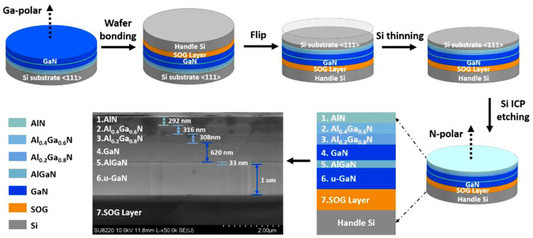
FIGURE 1. The schematic of obtaining N-polar Al(Ga)N films process through wafer bonding and substrate removal and the cross-sectional SEM picture of the bonded epi-layers.
Results and discussion
We first studied the ICP etching and the surface morphology of the exposed N-polar AlN/AlGaN/GaN layer. An Al-polar AlN (300 nm) sample grown on Si using the same growth process as that of the AlN buffer in Figure 1 1) and an Al/Ga polar Al0.3Ga0.7N (∼1.2 um) sample grown on sapphire were co-loaded with the N-polar sample to the ICP chamber. The etching process was conducted in BCl3/Cl2/Ar system at 20°C (table temperature) in vacuum chamber. The etch process on the N-polar AlN/AlGaN/GaN multilayer in Figure 2 was intentionally stopped on the Al0.4Ga0.6N layer (∼340 nm) and on the GaN layer (∼1020 nm) to study the surface morphology evolution. For the Al-polar AlN layers, the etched thickness was about 280 nm (because of the lower etch rate than N-polar Al(Ga)N under the same conditions in this experiment). For the Al-polar/Ga-polar Al0.3Ga0.7N layers, the etched thickness was about 340 nm. Figure 2 shows the OM images of the etched Al(Ga)N surfaces for both polarities after being placed in the same ambient (temperature = 24°C, humidity = 50%)for a certain period. Note that the OM images of the as-etched surfaces were recorded within 5 min after the samples taking out of the ICP chamber. One can see that all the etched N-polar samples exhibited dirty debris on their surfaces whereas the etched Al-polar/Ga-polar surfaces were smooth and clean. On the surface of the N-polar Al0.4Ga0.6N layer, the debris have a regular “+” shape. Interestingly, these dirty debris partially or completely disappeared after a period of time. However, the debris persisted on the N-polar GaN surface even after 30 days. The results were reproducible and repeatable after hundreds of times of experiments. The estimated debris density on the N-polar Al0.4Ga0.6N surface is about 7.8×10⁴/cm2in Figure 2 1) and associated with the etching conditions (e.g., varied gas flow rate, pressure, and ICP/RF power). The main ICP etching in Figure 2 was processed in a mixture of BCl3/Cl2/Ar (24/8/5 sccm) at 5 mtorr with ICP/RF power of 500 W/150 W. Higher gas flow rate and/or ICP power tended to increase the debris density (results not shown here). This unusual surface difference upon ICP dry etching between N- and Ga-polarities, to the best of our knowledge, has never been reported in the literature so far.
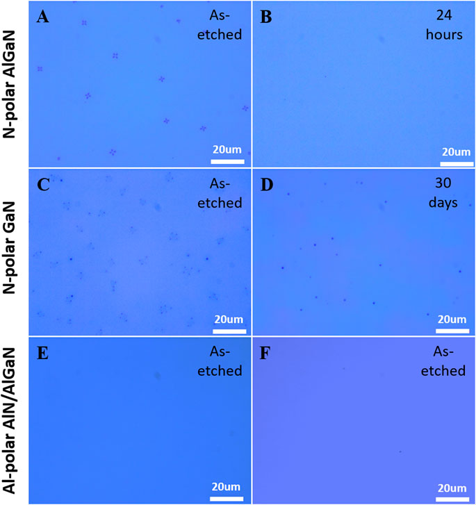
FIGURE 2. OM images of the N-polar AlGaN surface as-etched (A) and after placing in air for 1 day (B), the N-polar GaN surface as-etched (C) and placing in air after 30 days (D), and the as-etched Al-polar AlN surface (E) and the as-etched Al-polar AlGaN surface (F).
Meticulous inspections on the etched N-polar surface under OM at different time interval revealed that those surface debris did not exist just after sample taking out of chamber but soon appeared after exposing to air (temperature = 24°C, humidity = 50%) in a few minutes. As time elapsed, these surface debris then change gradually after a few hours or a few days. Figure 3 1)–3) clearly show the gradual appearance of the debris on the N-polar surface after the etching stopped on the Al0.4Ga0.6N layer (∼340 nm) and exposing in air for 50 s, 100 s, and 150 s, respectively. The OM images in Figure 3 4)–6) and the corresponding inserted AFM images recorded the disappearance of a specific surface debris at the same position (outlined by the red boxes) in a period of 8.5 h. The debris had an initial “+” shape and was ∼600 nm in height, resulting a RMS roughness of 95.1 nm in 5 × 5 μm2 (Figure 3D). Such a surface debris then slowly shrank and ultimately vanished after 8.5 h, only leaving a trace on the surface (Figure 3 (f)). Consequently, the RMS roughness within this area (5 × 5 μm2) is reduced to only 1.1 nm. It is also interesting to note that the surface debris did not completely disappear if the etch was stopped on the N-polar GaN layer (∼1020 nm), even after exposing in air for 42 days (see Figures 3G–I). As the AFM image showed in Figure 3I, the RMS roughness within this area (5 × 5 μm2) is about 1.6 nm. This implies that the debris evolution is affected by the Al composition of the surface layer.
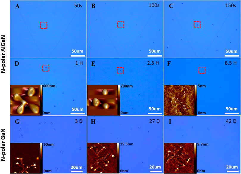
FIGURE 3. OM images showing the evolution process of surface debris when the etching was stopped on the Al0.4Ga0.6N layer (A–F) and on the GaN layer (G–I) after the samples were exposed in air for a certain period of time. The inserted are 5 × 5 μm2 AFM images around the debris region outlined by the red boxes in the corresponding OM images.
Figures 4A–C show the SEM images of one specific debris observed on the Al0.4Ga0.6N and on the GaN surface after etching and exposing in air for a few hours. The debris presented a clear “+” shape after etching to the AlGaN layer and exposing in air for 1 h. A clear trace can be seen on AlGaN and GaN surfaces when they were exposed in air for 3 h. To analyze the chemical composition of the debris, EDS of elements including Al, Ga, N, O and Cl were carried out. The result revealed that only the Cl distribution matches well with the shape of the debris, as observed in Figure 4 4)–(f). This implies that the appearance of debris on N-polar surface is due to the Cl-related byproduct during the etching process. Unfortunately, the distribution of oxygen on the etched surface observed under EDS did not show a specific accumulation in the debris region, which may be due to the detection limit of EDS. Then we used WDS (which has a higher resolution than EDS in testing trace elements) to analyze the distribution of O elements on the etched surface. Figure 4G shows the OM image of another specific debris observed on the Al0.4Ga0.6N after etching and exposing in air for 32 h. The previous classical “+” shape of debris has partially disappeared, leaving only a quarter of it. The WDS mappings in Figure 4 8)–1) indicate the debris contains not only Cl but also O element. Note that the OM and WDS images were taken in different time because of sample transferring.
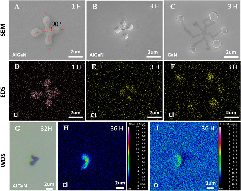
FIGURE 4. SEM images of surface debris when the etching was stopped on the Al0.4Ga0.6N layer (A) and (B) and on the GaN layer (C) after the samples exposing in air for a few hours. Fig.4 (D–F) are EDS mappings of Cl corresponding to the SEM image area in (A–C). Fig.4 (G) is the OM picture of surface debris when the etching was stopped on the Al0.4Ga0.6N layer after the samples exposing in air for 32 h. Fig.4 (H–I) are WDS mappings of Cl and O corresponding to the OM image in (G).
Next, three sets of experiment were carried out to investigate the influence of process gas on the surface morphology. Set (a) employed the same parameters as the previous etching process called conventional etching. Set (b) and (c) experiments added additional O2 and SF6 in the etching process, respectively. Other parameters were the same. For each set of experiment, a series of etching with different time was performed to monitor the etch rate and debris density variation on different layers. Seen in Figure 5, the additional O2 (3sccm) had a minor effect on the etch rate comparing Set (a) and Set (b). However, adding SF6 (3sccm) significantly slowed down the etch rate from 130 nm/min to 90 nm/min. This can be explained by the formation of nonvolatile AlF3 or GaF3 on the etching surface [31]. The surface morphologies after different etching time were immediately inspected after transferring out from ICP chamber. Figure 5 summarized the variation of surface debris density with etching time for each set of experiment. The debris density is calculated by counting the number of particles per unit area in the OM pictures. It can be seen that for Set (a) etching, the debris density increased dramatically with increasing etching depth and when the etch was stopped on the N-polar GaN surface, the debris density reached to ∼5×10⁵/cm2. However, adding a little amount of O2 or SF6 in the process gas effectively suppressed the generation of debris on the surface. When the etching was stopped on the AlN and Al0.4Ga0.6N layer, clean surfaces free of debris were successfully obtained. When etched to the Al0.2Ga0.8N and GaN layer, the debris cannot be completely eliminated but the density was still much lower than that in Set (a). Figure 6 shows the OM and AFM height images of the surfaces after the etching stopped on the Al0.4Ga0.6N layer (∼340 nm). The addition of O2 roughened the surface whereas the RMS surface roughness for the sample etched with additional SF6 was the lowest (∼0.56 nm).
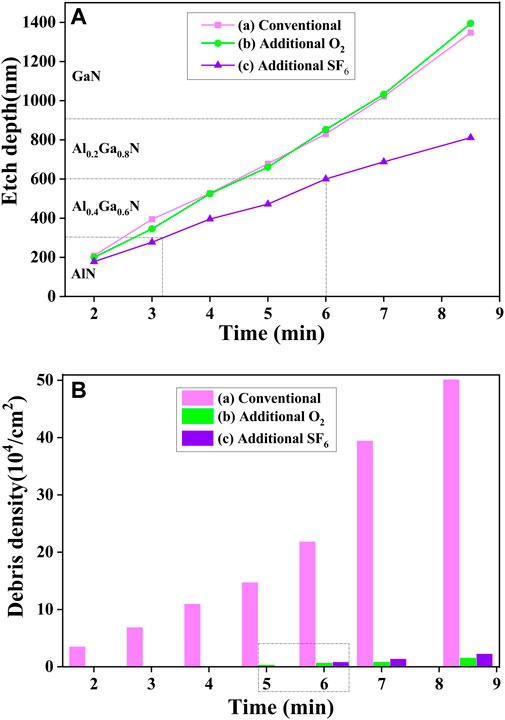
FIGURE 5. The (A) Etch depth and (B) Debris density of the etched N-polar AlxGa1-xN layers versus time with Conventional (a), Additional O2 (b) and Additional SF6 (c) etching in the BCl3 and Cl2 gases during the etching process.
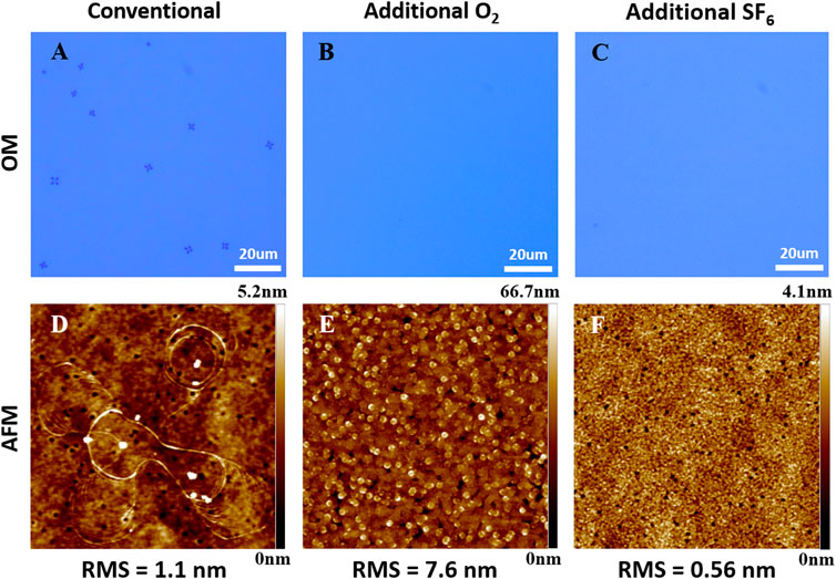
FIGURE 6. OM images of the surfaces with (A) Conventional and (B) Additional O2 and (C) Additional SF6 etching after the etching stopped at the Al0.4Ga0.6N layer; Fig.6 (D–F) are 5 × 5 μm2 AFM height images corresponding to the OM image areas in (A–C).
To completely eliminate the residue of debris on the N-polar GaN surface, an ICP “cleaning” process after the main ICP etching process was carried out. The main ICP etching was processed in a mixture of BCl3/Cl2/Ar (24/8/5 sccm) at 5 mtorr with ICP/RF power of 500 W/150 W. The etch process was finally stopped on the GaN layer (the etch depth is ∼1020 nm) and proceeded with a cleaning process in O2, SF6 and/or Ar plasmas. The ICP cleaning process was conducted at 5 mtorr with ICP/RF power of 750W/100 W at 20°C (table temperature). Table 1 listed the cleaning gas and flow rates for the four cleaning processes, i.e., C1–C4, that we have conducted. Figure 7 shows the OM images and the corresponding AFM height images for the etched GaN surfaces with four cleaning process. Compared to Figure 2 3) and Figure 3 (g), the debris on the etched N-polar GaN surface were eliminated completely. A clean surface free of debris can be obtained through a cleaning process with O2, SF6 or Ar with appropriate gas flow rate and cleaning duration (see Figure 7 5)–(h)). From the AFM height images, oxygen seems to roughen the surface morphology whereas SF6 and Ar can maintain a smooth surface (see Figure 7 1) - (L)) in the cleaning process while clearing away the debris. Compared C2 with C3, the cleaning effect by Ar was relatively weaker than SF6. Thus the cleaning time has to be extended to obtain a clean surface in C4. The RMS values in Figure 7 (j) and 7 (L) for C2 and C4 ICP clean are 0.66 nm and 0.59 nm, respectively, which are as smooth as the surface in Figure 6 (f).
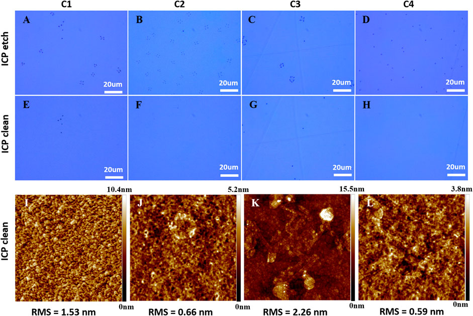
FIGURE 7. The OM images of the etched GaN surface after ICP etch (A–D) and after ICP clean (E–H) and the corresponding 5 × 5 μm2 AFM height images (I–L) with different ICP processes. The OM images were recorded just after the samples were transferred out from the ICP chamber.
So far we have shown that surface debris appeared on the N-polar Al(Ga)N layers etched by ICP with Cl-based gas after the samples were exposed in air. The debris can be self-disappeared partially or completely, depending on the Al composition of the surface layer. The EDS and WDS results suggested that the debris is the result of Cl-related byproduct generated during the etching process. In fact, it is already known that Al(Ga)Clx is the main byproduct generated during the ICP etching of Al(Ga)N films using BCl3/Cl2 gas. Such byproducts may not be desorbed timely during the etching and thus reside on the etched surface. It is also known that AlCl3 or GaCl3 can’texist stably in atmospheric environment and are susceptible to moisture. For example, when exposing in humid air, AlCl3 can be hydrated to form stable AlCl3⋅6H2O [32]. The regular “+” shaped morphology as observed in Figure 2 1) and Figure 4 1) indicates a crystallization process on the surface. In addition, the EDS and WDS results revealed that the debris contains both Cl and O. Therefore, it is highly likely that such regular shaped debris are just AlCl3⋅6H2O crystals. In addition, we only observed such crystallization on the etched N-polar surface rather than on the etched Al-polar surface, implying that the N-polar surface has a higher absorbance of the Al(Ga)Clx byproducts than the Al-polar surface. This may be due to the different surface activeness between N-polar and Al-polar/Ga-polarities [33]. In the ambient environment, the AlCl3⋅6H2O crystals are then gradually decomposed to release HCl gas [34], which can be verified by the loss of Cl in accordance with the shrinkage of debris on the surface seen in Figure 4 (b). Such a process is previously attributed to the cause of the formation of “worm”-like residuals after ICP etch of Al [34]. The difference is that after the Al dry etch, the generated HCl reacts with Al to form AlCl3 which further reacts with moisture and generate HCl again, leading to a continuous corrosion of the Al surface. The more debris residuals on the GaN surface than that on the AlN surface implies that GaCl3⋅6H2O is more stable than AlCl3⋅6H2O.
Adding O2 or SF6 in the process gas or with additional cleaning process helps remove the Al(Ga)Clx byproducts on the surface. There are two mechanisms involved. First, O2 and SF6 can react with Ga(Al)Clx and convert it the Ga(Al)Ox which reduces the Cl byproducts coverage on the surface. Second, the physical bombardment by O, F or Ar plasmas also contributes to the Cl byproducts removal. Therefore, in terms of the surface cleaning effectiveness, O2 and SF6 are more effective than Ar. However, it has been reported that F− ions may be implanted in the GaN film and physical bombardment can cause surface defects, and both can result in device reliability issue. Further studies are needed to comprehensively evaluate the cleaning process influence on the device performance and reliability.
Finally, the physicochemical mechanisms of debris’ formation and disappearance on N-polar GaN with conventional etch conditions in Figure 7 1) are illustrated in Figure 8. There are six steps: Step 1 is the neutral chlorine absorbance on the N-polar GaN, Step 2 is the reaction of Cl and GaN to produce byproduct such as GaClx, Step 3 is the ion bombardment of GaClx micelles by Ar+ or Clx+, Step 4 is the partial desorption of GaClx from gaseous GaClx, Step 5 is the gradual crystallization of GaClx·6H2O in an ambient environment. The sixth step reveals the GaClx·6H2O micelles’ spontaneous decomposed reaction process: GaClx·6H2O→GaxOy + xHCl↑ [34]. Therefore, the reduction of the Cl-byproduct coverage on the surface is the key for obtaining smooth and uniform etching for N-polar Al(Ga)N layers.
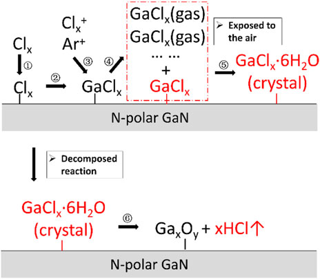
FIGURE 8. The Physicochemical mechanism of particles’ formation and disappearance on N-polar GaN with conventional etch conditions in Figure 7 (a).
Conclusion
We have investigated the ICP etching on the N-polar Al(Ga)N layers obtained from wafer bonding and layer transfer. It is found that surface debris appeared on the N-polar surface after exposed to the air for a short period whereas that was not observed on the Al-polar/Ga-polar surface. The debris can be completely self-vanished on the N-polar surface of Al0.4Ga0.6N layer after exposing in air for a few hours but persisted on the N-polar GaN surface. The EDS result suggested that the debris is the result of Cl-related byproduct generated during the etching process. The WDS results also confirmed that the debris contained both Cl and O elements. It is believed that byproducts like Al(Ga)Clx cannot desorbed timely from the N-polar surface during the etching. When the etched sample is removed from the ICP reaction chamber, the residual Al(Ga)Clx on the etched N-polar surface will absorb moisture to form Al(Ga)Clx·6H2O and rapidly crystallize due to exposing in air. The Al(Ga)Clx·6H2O crystal then releases HCl gas, leaving Al(Ga)xOy on the etched surface. Adding O2 or SF6 in the process gas or with additional cleaning process help remove the Al(Ga)Clx byproducts on the surface, therefore a clean and smooth N-polar GaN surface at reasonable etching rate can be successfully obtained.
Data availability statement
The original contributions presented in the study are included in the article/supplementary materials, further inquiries can be directed to the corresponding author.
Author contributions
XG, CL and ZC contributed to conception and design of the study. XY organized the database. QZ, QF, WXH and QL performed the statistical analysis. XG wrote the first draft of the manuscript. XG and CL wrote sections of the manuscript. All authors contributed to manuscript revision, read and approved the submitted version.
Funding
This work is supported by the National Natural Science Foundation of China (62004049, 6210032639), the Guang dong Academy of Sciences (2021GDASYL-20210103077, 2019GDASYL-0102008) and the Key-Area Research and Development Program of Guangdong Province (2020B010173001, 2020B010174001).
Acknowledgments
The authors would like to thank the Nano Fabrication Facility, Consigned processing for Wafer bonding and CMP process, Micromachining and device platform, Songshan Lake Materials Laboratory.
Conflict of interest
The authors declare that the research was conducted in the absence of any commercial or financial relationships that could be construed as a potential conflict of interest.
Publisher’s note
All claims expressed in this article are solely those of the authors and do not necessarily represent those of their affiliated organizations, or those of the publisher, the editors and the reviewers. Any product that may be evaluated in this article, or claim that may be made by its manufacturer, is not guaranteed or endorsed by the publisher.
References
1. Wong MH, Keller S, Nidhi SD, Denninghoff DJ, Kolluri S, Brown DF, et al. N-polar GaN epitaxy and high electron mobility transistors. Semicond Sci Technol (2013) 28:074009. doi:10.1088/0268-1242/28/7/074009
2. Rakoski A, Diez S, Li H, Keller S, Ahmadi E, Kurdak Ç. Electron transport in N-polar GaN-based heterostructures. Appl Phys Lett (2019) 114:162102. doi:10.1063/1.5090233
3. Romanczyk B, Zheng X, Guidry M, Li H, Hatui N, Wurm C, et al. W-band power performance of SiN-passivated N-polar GaN deep recess HEMTs. IEEE Electron Device Lett (2020) 41:349–52. doi:10.1109/led.2020.2967034
4. Park PS, Rajan S. Simulation of short-channel effects in N-and Ga-polar AlGaN/GaN HEMTs. IEEE Trans Electron Devices (2011) 58:704–8. doi:10.1109/ted.2010.2099121
5. Karrer U, Ambacher O, Stutzmann M. Influence of crystal polarity on the properties of Pt/GaN Schottky diodes. Appl Phys Lett (2000) 77:2012–4. doi:10.1063/1.1313275
6. Kwak JS, Lee KY, Han JY, Cho J, Chae S, Nam OH, et al. Crystal-polarity dependence of Ti/Al contacts to freestanding n-GaN substrate. Appl Phys Lett (2001) 79:3254–6. doi:10.1063/1.1419053
7. Singisetti U, Wong MH, Dasgupta S, Swenson NB, Thibeault BJ, et al. Enhancement-mode N-polar GaN MISFETs with self-aligned source/drain regrowth. IEEE Electron Device Lett (2011) 32:137–9. doi:10.1109/led.2010.2090125
8. Abou Daher M, Lesecq M, Tilmant P, Defrance N, Rousseau M, Cordier Y, et al. AlGaN/GaN high electron mobility transistors on diamond substrate obtained through aluminum nitride bonding technology. J Vacuum Sci Tech B (2020) 38:033201. doi:10.1116/1.5143418
9. Sun Q, Cho Y, Lee I-H, Han J, Kong B, Cho H. Nitrogen-polar GaN growth evolution on c-plane sapphire. Appl Phys Lett (2008) 93:131912. doi:10.1063/1.2993333
10. Brown DF, Chu R, Keller S, DenBaars SP, Mishra UK. Electrical properties of N-polar AlGaN/GaN high electron mobility transistors grown on SiC by metalorganic chemical vapor deposition. Appl Phys Lett (2009) 94:153506. doi:10.1063/1.3122347
11. Rajan S, Wong M, Fu Y, Wu F, Speck JS, Mishra UK. Growth and electrical characterization of N-face AlGaN/GaN heterostructures. Jpn J Appl Phys (2008) (2005) 44:L1478–80. doi:10.1143/jjap.44.l1478
12. Keller S, Fichtenbaum N, Wu F, Brown D, Rosales A, DenBaars S, et al. Influence of the substrate misorientation on the properties of N-polar GaN films grown by metal organic chemical vapor deposition. J Appl Phys (2007) 102:083546. doi:10.1063/1.2801406
13. Chung JW, Piner EL, Palacios T. N-face GaN/AlGaN HEMTs fabricated through layer transfer technology. IEEE Electron Device Lett (2008) 30:113–6. doi:10.1109/led.2008.2010415
14. Yu Z, Zhang L, Yu G, Deng X, Jiang C, Tang W, et al. High quality of N-polar GaN film fabricated by layer transfer technology using high selective material removal rate of CMP. Mater Sci Semiconductor Process (2022) 141:106440. doi:10.1016/j.mssp.2021.106440
15. Smith MD, Li X, Uren MJ, Thayne IG, Kuball M. Polarity dependence in Cl2-based plasma etching of GaN, AlGaN and AlN. Appl Surf Sci (2020) 521:146297. doi:10.1016/j.apsusc.2020.146297
16. Ryu KK, Roberts JC, Piner EL, Palacios T. Thin-body N-face GaN transistor fabricated by direct wafer bonding. IEEE Electron Device Lett (2011) 32:895–7. doi:10.1109/led.2011.2147751
17. Able A, Wegscheider W, Engl K, Zweck J. Growth of crack-free GaN on Si (1 1 1) with graded AlGaN buffer layers. J Cryst Growth (2005) 276:415–8. doi:10.1016/j.jcrysgro.2004.12.003
18. Zhou R, Feng M, Wang J, Zhong Y, Sun Q, Liu J, et al. Effect of surface stoichiometry on the non-alloyed ohmic contact to N-face n-GaN. Solid-State Elect (2020) 171:107863. doi:10.1016/j.sse.2020.107863
19. Li D, Sumiya M, Fuke S, Yang D, Que D, Suzuki Y, et al. Selective etching of GaN polar surface in potassium hydroxide solution studied by x-ray photoelectron spectroscopy. J Appl Phys (2001) 90:4219–23. doi:10.1063/1.1402966
20. Song IJ, Lee SK, Lee K, Park SS, Han JY. Properties of etched Ga-and N-faces of freestanding GaN substrate using inductively coupled plasma-reactive ion etching. Jpn J Appl Phys (2008) (2002) 41:L317–9. doi:10.1143/jjap.41.l317
21. Liu X, Sun C, Xiong B, Niu L, Hao Z, Han Y, et al. Smooth etching of epitaxially grown AlN film by Cl2/BCl3/Ar-based inductively coupled plasma. Vacuum (2015) 116:158–62. doi:10.1016/j.vacuum.2015.03.030
22. Shah AP, Rahman AA, Bhattacharya A. ICP-RIE etching of polar, semi-polar and non-polar AlN: Comparison of Cl2/Ar and Cl2/BCl3/Ar plasma chemistry and surface pretreatment. Semicond Sci Technol (2015) 30:015021. doi:10.1088/0268-1242/30/1/015021
23. Guo W, Xie J, Akouala C, Mita S, Rice A, Tweedie J, et al. Comparative study of etching high crystalline quality AlN and GaN. J Cryst Growth (2013) 366:20–5. doi:10.1016/j.jcrysgro.2012.12.141
24. Rizzi F, Gu E, Dawson M, Watson IM, Martin RW, Kang XN, et al. Thinning of N-face GaN (0001) samples by inductively coupled plasma etching and chemomechanical polishing. J Vacuum Sci Tech A: Vacuum Surf Films (2007) 25:252–60. doi:10.1116/1.2433987
25. Waki I, Iza M, Speck JS, Denbaars SP, Nakamura S. Etching of Ga-face and N-face GaN by inductively coupled plasma. Jpn J Appl Phys (2008) (2006) 45:720–3. doi:10.1143/jjap.45.720
26. Shah AP, Rahman AA, Bhattacharya A. Temperature-dependence of Cl 2/Ar ICP-RIE of polar, semipolar, and nonpolar GaN and AlN following BCl 3/Ar breakthrough plasma. J Vacuum Sci Tech A (2020) 38:013001. doi:10.1116/1.5123787
27. Keller S, Dora Y, Chowdhury S, Wu F, Chen X, DenBaars SP, et al. Growth and characterization of N-polar GaN and AlGaN/GaN HEMTs on (111) silicon. Phys Status Solidi C (2011) 8:2086–8. doi:10.1002/pssc.201000958
28. Dragoi V, Glinsner T, Mittendorfer G, Wieder B, Lindner P. Adhesive wafer bonding for MEMS applications. Smart Sensors, Actuators, and MEMS (2003) 5116:160–7.
29. Xianshu L, Yulian C, Junfeng S, Xiaonan H, Yuanbing C, Chengming L, et al. High-throughput multiple dies-to-wafer bonding technology and III/V-on-Si hybrid lasers for heterogeneous integration of optoelectronic integrated circuits. Front Mater (2015) 2:28. doi:10.3389/fmats.2015.00028
30. Osipov AA, Speshilova AB, Endiiarova EV, Alexandrov S. Dry etching of silicon carbide in ICP with high anisotropy and etching rate. In: IOP Conference Series: Materials Science and Engineering. IOP Publishing (2020). p. 022039.
31. Pearton SJ, Zolper JC, Shul RJ, Ren F. GaN: Processing, defects, and devices. J Appl Phys (1999) 86:1–78. doi:10.1063/1.371145
32. Cameron G, Chambers A. Successfully addressing post-etch corrosion. Semiconductor Int (1989) 12:142–7.
33. Li S, Wang X, Mohajerani MS, Fündling S, Erenburg M, Wei J, et al. Dependence of N-polar GaN rod morphology on growth parameters during selective area growth by MOVPE. J Cryst Growth (2013) 364:149–54. doi:10.1016/j.jcrysgro.2012.11.027
Keywords: Al(Ga)N, N-polar, ICP etching, surface roughness, byproducts
Citation: Ge X, Yin X, Zeng Q, Feng Q, Wang X, Li Q, Chen Z and Li C (2022) Study of dry etched N-polar (Al)GaN surfaces obtained by inductively coupled plasma etching. Front. Phys. 10:1042998. doi: 10.3389/fphy.2022.1042998
Received: 13 September 2022; Accepted: 10 October 2022;
Published: 26 October 2022.
Edited by:
Renchun Tao, Peking University, ChinaReviewed by:
Siliang He, Guilin University of Electronic Technology, ChinaZhihong LIU, Xidian University, China
Copyright © 2022 Ge, Yin, Zeng, Feng, Wang, Li, Chen and Li. This is an open-access article distributed under the terms of the Creative Commons Attribution License (CC BY). The use, distribution or reproduction in other forums is permitted, provided the original author(s) and the copyright owner(s) are credited and that the original publication in this journal is cited, in accordance with accepted academic practice. No use, distribution or reproduction is permitted which does not comply with these terms.
*Correspondence: Chengguo Li, Y2hlbnpoaXRhb0BnZGlzaXQuY29t, bGljaGVuZ2d1b0B1Lm51cy5lZHU=
 Xiaoming Ge1
 Xuebing Yin
 Chengguo Li