
94% of researchers rate our articles as excellent or good
Learn more about the work of our research integrity team to safeguard the quality of each article we publish.
Find out more
ORIGINAL RESEARCH article
Front. Phys. , 07 November 2022
Sec. Optics and Photonics
Volume 10 - 2022 | https://doi.org/10.3389/fphy.2022.1019113
This article is part of the Research Topic Recent Developments in Si-based Materials and Devices View all 8 articles
We present the detailed numerical analysis and characterization of SiGe/Si heterojunction electro-optic modulator at 2 μm, 4.3 μm, and 5 μm wavelengths. We investigate the band, the refractive index, and the carrier injection efficiency of SiGe/Si heterojunction PIN electrical structure. Numerical investigations are carried out on the key geometrical parameters, doping concentration, Ge content. The results show that the modulated voltage of SiGe/Si PIN heterojunction modulator is lower 50% than that of Si modulator under the same modulation effect. In order to eliminate the absorption losses of SiO2 in mid-infrared, the punch Mach–Zehnder optical structure is established and researched. The research present that the modulator has the short 500 µm phase shifters and the low VπLπ of 0.042 Vcm under forward bias voltage, and the extinction ratio is greater than 12.81 dB. The high-speed transmission characteristics are shown to have clean eye diagrams up to 40 Gbps in mid-infrared.
Silicon-based photonic modulators in the near-infrared (NIR) have received a lot of attention in the last decade; however, to meet the growing demand for transmission capacity, it is necessary to extend the wavelength to the mid-infrared (MIR) spectrum of 2–20 µm. The MIR band is expected to be used in applications such as environmental monitoring, bio sensing, and free optical communication [1–5]. Silicon on insulator (SOI), the most studied platform in the NIR and MIR, has been demonstrated in recent years with several low-loss silicon MIR waveguides operating at 2–8 µm [6–11]; several MIR passive and active devices have also been demonstrated, including grating couplers [12, 13], multimode interferometers (MMI) [7, 14], Array Waveguide Gratings (AWG) [15], and germanium-tin photodetectors [16], which make MIR communication possible. However, the oxide layer of the SOI platform has great absorption in the MIR, so many research mechanisms have overcome this problem by designing waveguides. In 2016, Penades designed a suspended MIR SOI waveguide SWG device, which has a waveguide transmission loss of 0.85 dB/cm at 3.8 µm wavelength by optimizing the structure size and fabrication process of the waveguide [17]. The design of this suspended waveguide structure well avoids the high loss of the device due to the contact between the waveguide and BOX, and the experiment also has been demonstrated the great potential of subwavelength grating devices for MIR wavelength applications. Meanwhile, some other silicon-based platforms with extended spectral transparency have been reported in the MIR, such as sapphire-on-silicon [18], silicon-on-germanium platforms [19], using SiGe on a silicon substrates [20], and so on.
At present, the modulation rate of modulators with traditional silicon materials has been reached to 50 Gb/s, but it is difficult to further increase the modulation rate. Compared with Si material, SiGe material has higher carrier mobility, been compatible with CMOS process, and strong Electric Absorption (EA) effect. The SiGe material is an ideal material, which has the advantages of large modulation bandwidth, high modulation efficiency, high extinction ratio and low insertion loss, and has a bright application prospects in the MIR. The plasma-dispersion-effect, which changes the refractive index of the material by changing the carrier concentration in the material, is currently the most practical modulation mechanism in silicon-based modulators. In 2018, Wang designed a silicon modulator based on the plasma-dispersion-effect operating at 2 µm wavelength [21]. Although their research showed that the modulator can be operated at 2 μm wavelength, the modulation rate of the device needs to be further optimized. At the same time, compared with the modulator based on Group IV materials, this silicon modulator has the characteristics of compatibility with CMOS process and low cost, but its modulation performance is still far from enough [22]. The above results show that the use of modulators based on the plasma-dispersion-effect in the NIR has the advantage of compatibility with CMOS processes, there are still many problems for applications in the MIR. For example, in the MIR, because of the opacity of Si material and the strong absorption of SiO2, how to select the waveguide material and develop the waveguide structure with low loss have become the key problems in the research and development of the MIR modulator. In 2011, Nedeljkovic’s research showed that the plasma-dispersion-effect is more significant in the MIR than in the NIR. In this case, the carriers injection will lead to higher loss of devices operating in the MIR [23]. Especially for the Mach-Zehnder structure, the optical loss caused by carrier absorption will also reduce the extinction ratio of the device.
We design and simulate a SiGe/Si heterojunction PIN modulator with the punch Mach-Zehnder structure, and the detailed numerical analysis and characterization are carried out at 2 μm, 4.3 μm, and 5 μm. After many simulation optimizations on the size of the modulator, and the most suitable parameter settings are obtained, the design of this Mach-Zehnder modulator mainly consists of two parts. In order to reduce the absorption of SiO2 in the MIR and reduce the overall loss of the modulator, an air layer is formed between the flat plate layer of the MZ modulator and the buried SiO2 layer by etching. Compared with silicon, the carrier injection type MZ modulator designed in this paper has a waveguide region composed of SiGe material, and a large number of carriers can be injected into the waveguide region at the same applied bias voltage.
Plasma-dispersion-effect refers to the phenomenon of introducing free carriers into the optical transmission medium and changing the optical properties of the optical transmission medium. For silicon-based materials, the effective refractive index and absorption coefficient of the silicon waveguide can be changed by introducing free carriers into the silicon waveguide and doping a certain concentration of P-type and N-type. Theoretically, the modulation rate of silicon-based electro-optic modulator based on plasma-dispersion-effect can reach more than several tens of GHz or more. At present, silicon-based high-speed electro-optic modulator is basically designed based on the plasma-dispersion-effect.
In order to quantitatively calculate the effective refractive index of silicon material for optical signals, we need to consider the distribution of carriers in silicon. The distribution of carriers in silicon material should consider the doping region and concentration, carrier drift and diffusive motion under the applied bias, etc. The overall effective refractive index change on the basis of non-perturbation index can be calculated from the total carrier density as follows:
where n,p are the carrier densities of electrons and holes, respectively, and εm is the dielectric constant of the unperturbed material; me,mh are the effective masses of electrons and holes, respectively; ue,uh are the mobilities of electrons and holes.
Assuming a specific wavelength of the composite refractive index, the extension of the Drude model described above can also be derived from the variation of the carrier density of most semiconductors. However, the model of Soref et al can more accurately describe the effect of carrier density on refractive index in silicon. In this model, Soref introduces the wavelength of the optical signal passing through the silicon material as an important influence factor. The effective refractive index and absorption coefficient change with the wavelength of the optical signal. Obviously, this model is more accurate than Drude [24]. According to the experimental results of refractive index and optical absorption spectrum obtained by Soref et al., the empirical formula for the change of refractive index and absorption coefficient are obtained [25, 26]:
In the above equation, e is the electronic charge,
where n is the real part of the refractive index and α is the absorption coefficient; ∆ne is the change in refractive index due to electrons and ∆nh is the change in refractive index due to holes; ∆αe is the change in the absorption coefficient due to electrons and ∆αh is the change in the absorption coefficient due to holes; Ne is the concentration of electrons (cm−3) and Nh is the concentration of holes (cm−3).
Since SiGe material is an alloy of Si and Ge, the refractive index of SiGe can be expressed as [27]:
where
From (Eq. 7, 8), it can be seen that in the MIR, the absorption coefficient change
For the silicon-based electro-optic modulator based on the plasma-dispersion-effect, we control the injection efficiency of free carriers into the waveguide by adjusting the forward bias voltage of PIN junction to change the carrier concentration and the effective refraction of the waveguide. The relationship between the effective refractive index difference of the waveguide and the phase shift of the optical signal passing through the waveguide [28] is shown in (Eq. 9):
where L is the modulator length; λ0 is the optical wavelength; and Δneff is the effective refractive index difference. The π-phase shift can be achieved by adjusting the voltage, which is defined as Vπ.
The distance from the doped region to the ridge waveguide region has a great influence on the attenuation of the optical signal. The carrier absorption loss [28] is related to the imaginary part (k) of the effective refractive index within the ridge waveguide, as shown in (Eq. 10):
Due to the inherent carrier absorption loss of SiO2 in the MIR, the design of the device structure becomes a key factor in reducing device losses. The design of small size is also very important, because larger device size often leads to higher capacitance of the device, which limits the modulation rate of the device or causes the device to have higher modulation loss. To overcome these problems, we demonstrate a SiGe/Si heterojunction MZ modulator with a lateral PIN structure. The electrical structure of the SiGe/Si PIN heterojunction modulator is shown in Figure 1. When optical wave is propagated into the modulation region of the modulator, which is also absorbed by the SiGe modulation region, and the amount of absorption depends on the forward bias voltage of modulator. The lateral PIN structure has a narrow intrinsic SiGe/Si region to achieve high extinction ratios at low voltage. The main purpose is to reduce the overall power consumption of the device and improve the modulation efficiency.

FIGURE 1. Electrical structure of SiGe/Si PIN heterojunction modulator. (A) three-dimensional schematic and (B) cross-sectional schematic.
In Figure 1A, the blue area represents SiGe, the orange area represents Si, the green area represents SiO2, the yellow area represents the metal electrode, and the gray area represents air. In Figure 1B, the cross-sectional width of the device is W, H is the height of the ridge waveguide, h is the height of the slab, Ws is the distance between the ridge waveguide region and the doping concentration region, and Wr is the width of the ridge waveguide. The SiGe/Si heterojunction ridge waveguide based on SOI substrate has a SiGe/Si layer with a thickness of 220 nm/500 nm on the top and a SiO2 buried oxide layer with a thickness of 2 μm at the bottom. Air layer of suspended waveguide structure has also been used in silicon modulator, but this structure is prone to collapse when other layers are made on top of the waveguide layer. We designed the structure not only to reduce the absorption loss of SiO2 layer, but also can better support the top waveguide and prevent the collapse of the top structure. In the actual fabrication process, low refractive index materials, such as deposition Si3N4, can be used in the upper cladding layer (air layer) on the device to play the role of isolation and protection.
The metal is connected to the anode (P+) and cathode (N+), as showed in Figure 1B. The doping concentration of N+ and P+ ranges from 1e17 cm−3 to 1e19 cm−3, and the I region is N-type doping of 1e15 cm−3.
As shown in Figure 1, a PIN modulation structure with Si/SiGe/Si heterojunction is designed in this paper. The new suspension structure can effectively reduce the modulation power consumption and improve the modulation efficiency of the device. Using SiGe heterojunction structure, not only reduce the absorption loss of SiO2 layer, but also can better support the top waveguide and prevent the collapse of the top structure. The structure is compatible with CMOS process, and the process flow of the waveguide structure is shown in Figure 2.
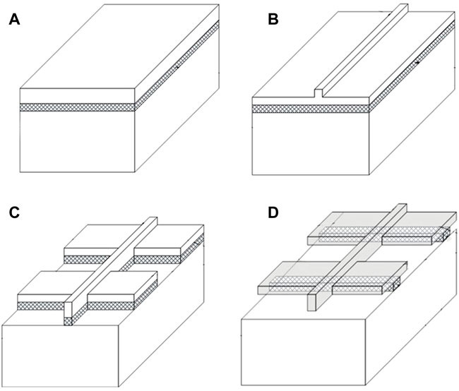
FIGURE 2. SiGe/Si waveguide structure process flow diagram. (A) SiGe/Si heterojunction OI substrate. (B) SiGe/Si heterojunction ridge waveguide structure. (C) Lithography. (D) Suspended SiGe/Si heterojunction waveguide structure.
Figure 3 shows the schematic optical structure of SiGe/Si PIN heterojunction MZ modulator, which is belonged to Mach-Zehnder optical modulation structure [29]. By applying the forward bias voltage to the upper arm of the phase shifter, the refractive index of the waveguide region is changed to achieve modulation. In order to reduce the device loss and size, the length of the phase shifter is set to 500 μm based on previous design experience.
In Figure 1, the electrical structure is designed consists of highly doped P-type and N-type Si, and intrinsic N-type SiGe. The structure can be equivalently considered as having a Pn heterojunction and an nN heterojunction. Since the PIN is working, the carriers of I-region come from the electrons of N-region and the holes of P-region, respectively, and the barrier height is the key to affecting the injection efficiency of electrons and holes. Therefore, it is particularly important to analyze the Pn hole barrier height and the nN electron barrier height in this structure. According to previous research of our group [30], at a certain temperature, for Pn heterojunctions, the lower doping concentration of P-region, the smaller hole barrier height; the smaller band gap, the larger intrinsic carrier concentration, the smaller hole barrier height; the larger Ge content, the smaller hole barrier height. For nN heterojunctions, the lower doping concentration of N-region, the higher doping concentration of n-region, the smaller electron barrier height; the larger band gap of n-region, the smaller intrinsic carrier concentration, the smaller electron barrier height; the smaller band gap of the N-region, the greater intrinsic carrier concentration and the smaller electron barrier height; the smaller Ge content, the smaller electron barrier height. After a forward bias voltage is set on PIN device, the balance between the original carrier offset and the diffusion movement is destroyed, and PIN device is in the non-equilibrium state. Since the doping concentration of I-region is small, I-region has a high resistance, and both the P-region and the N-region are highly doped, so the resistance is very low. Therefore, the forward bias is basically in the I-region. The forward bias generates an electric field to the built-in electric field in the I-region opposite, thus the electric field is weakened in the I-region, reducing the space charge and the barrier height. Since the hole barrier height of Pn heterojunction and the electron barrier height of nN heterojunction are all small in the equilibrium state, the barrier height of Si/SiGe/Si is first flattened, so that I-region of PIN device has greater carrier injection under the same applied voltage.
Using the commercial numerical simulation software CHARGE, MODE and INTERCONNECT based on Lumerical Company, the electrical and optical performance optimization and high-speed photoelectric modulation performance simulation of the designed MZ modulator are carried out. In this work, the CHARGE tool was used to calculate the change in carrier concentration in the waveguide region. The calculated carrier concentration was inserted into the MODE tool to solve the optical transmission properties of SiGe waveguides under fundamental mode conditions. Finally, insert the results calculated by the MODE tool into the INTERCONNECT tool to form a complete MZ modulator by cascading devices, and analyze the performance of the SiGe heterojunction MZ modulator under high-speed signals.
It can be concluded from (Eq. 6) that the refractive index of SiGe material is proportional to Ge content. The change in Ge content will directly lead to the change in refractive index and the energy band of SiGe material. Figure 4 shows Ge content versus the carrier injection concentration in the waveguide region at a forward bias voltage of 2 V. It can be seen from the figure that the carrier concentration of SiGe/Si PIN heterojunction modulator is significantly higher than that of Si modulator. The carrier concentration in the waveguide region increases rapidly with increasing Ge content after the forward bias voltage is higher than 0.7 V, and with a Ge content of 40%, the carrier concentration in the waveguide region is about 1.32e19 cm−3 at a bias voltage of 2 V. However, a large amount of carrier injection in the waveguide region will result in the higher carrier absorption loss.
Figure 5 shows the relationship between Ge content and the absorption coefficients at 2 μm wavelength. It can be seen from the figure that due to the increase of Ge content, the absorption coefficient of phase shifter continues to increase. It can also be seen from formula (Eq. 3) that when the input wavelength is constant, the absorption coefficient of phase shifter will increase with the increase of refractive index of SiGe material. At the same time, when the refractive index of SiGe material is constant, so the Ge content is constant, and the absorption coefficient of phase shifter will increase with the increase of input wavelength.
Therefore, in order to reduce device loss, we choose the Ge content to be 20%. Under forward bias voltage of 2 V, the carrier injection concentration of waveguide region can be up to 7.2e18 cm−3.
The effect of different doping concentrations on the modulator performance is simulated, as showed in Figure 6A. Figure 6A scans the relationship between the carrier injection concentration of SiGe waveguide region and the forward bias voltage under the doping concentration of 1e17 cm−3∼1e19 cm−3. It can be seen from the figure that the carrier concentration of SiGe waveguide region increases rapidly with increasing the forward bias voltage when the voltage is higher than 0.7 V. The carrier injection concentration of SiGe waveguide region also increases with the increase of doping concentration under the same bias voltage. Accordingly, due to the large number of carriers injection, it is inevitable that the waveguide region will have a higher carrier absorption loss. Figure 6B is based on the Soref model, and the effect of electrons and holes on Δn (the effective refractive index difference coefficient) is calculated. It can be seen from the calculation results that when the doping concentration reaches to 1e18 cm−3 or more, the effective refractive index difference coefficient will reach to 10−3. Therefore, in order to avoid high loss of device, the carrier concentration of P-region and N-region is finally selected as 1e18 cm−3.
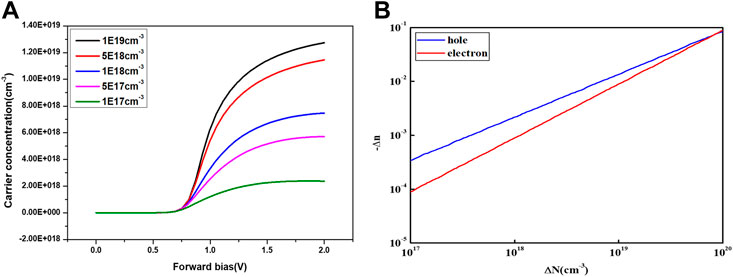
FIGURE 6. (A) Relationship between doping concentration and carrier injection concentration. (B) Variation curve of carrier concentration and Δn.
Next, the position of P-region and N-region was optimized by simulation, as showed in Figure 7. From the empirical formula of the plasma-dispersion-effect, it can be known that electrons and holes have different abilities to change the refractive index and absorption coefficient of SiGe waveguide region, so determining Ws can appropriately reduce the transmission loss of the device. By parametrically scanning the effect of different Ws on the carrier injection concentration of SiGe waveguide region, it can be seen from the figure that when the doping concentration of P-region and N-region are 1e18 cm−3, the carrier injection concentration of SiGe waveguide region decreases continuously with the increase of Ws. At the same voltage, the smaller Ws, the higher the transmission loss of the device, due to the increased carrier injection concentration of SiGe waveguide region. When Ws is greater than 0.8 μm, the carrier injection concentration of SiGe waveguide region changes little, while Ws is less than 0.8 μm, the carrier injection concentration increases rapidly in SiGe waveguide region. Therefore, it is necessary to select a compromise value in the range of 0.6∼1 μm, and finally Ws is selected as 0.8 μm.
After the above simulation analysis, we determined that Ge content is 20% in the SiGe alloy material, the doping concentration of the P-region and N-region are 1e18 cm−3, the I region is N-type lightly doped, the doping concentration is 1e15 cm−3, and the distance Ws between the doping region and SiGe waveguide region is 0.8 μm. Next, we mainly carried out the simulation optimization of the system based on the single-mode and single-bias waveguide to find the optimal size of the SiGe waveguide. The ridge-type waveguide structure is adopted, and the optical field energy can be limited in SiGe waveguide layer. Respectively, we obtained the relationship between the effective refractive index and the ridge width (Wr) of Si waveguides and SiGe waveguides with Ge content of 20% at 2 μm, 4.3 μm and 5 μm, as shown in Figure 8.
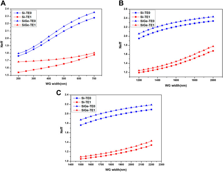
FIGURE 8. Simulation curves of effective refractive index and ridge width of Si waveguide and SiGe waveguide at (A) 2 μm wavelength, (B) 4.3 μm wavelength and (C) 5 μm wavelengths.
It can be seen from the figure that the effective refractive index of waveguide increases continuously with the increase of the width of waveguide. At 2 μm wavelength, when Wr increases to 600 nm, the effective refractive index of waveguide with the high-order modes has a sharp increase trend. Similarly, when the operating wavelength is 4.3 μm and 5 μm, Wr increases to 1500 nm and 1800 nm, respectively. At this time, there is a rapid increase of high-order modes, while the change region of fundamental-order modes is gentle. Therefore, as the waveguide width increases, it will inevitably cause the appearance of higher order modes in the waveguide, which affects the single-mode and single-bias transmission characteristics of waveguide. However, the reduction of Wr will also make the waveguide unable to completely limit the optical field energy, resulting in energy leakage from waveguide, and also increase the transmission loss of waveguide. Therefore, in order to obtain a single-mode and single-bias transmission waveguide with lower loss, Wr is set to 600 nm, 1500 nm and 1800 nm at 2 μm, 4.3 μm and 5 μm wavelengths, respectively.
After the ridge waveguide width are confirmed at 2 μm, 4.3 μm, and 5 μm wavelengths, in order to further optimize the size of the ridge waveguide to obtain a waveguide structure with low transmission loss, the optimization of the slab height is also an important part of the waveguide design. It will also affect the ability of the waveguide to limit the optical field energy. We simulated the relationship between the carrier absorption loss and the phase shift of SiGe waveguide with different slab height at 2 μm, 4.3 μm, and 5 μm wavelengths, as showed in Figure 9.
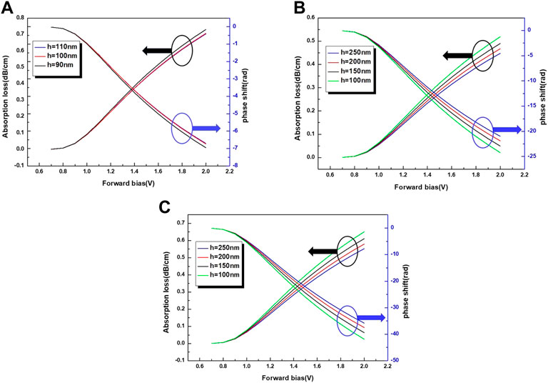
FIGURE 9. Bias voltage vs. carrier absorption loss and simulated phase shift in the waveguide region at (A) 2 μm wavelength, (B) 4.3 μm wavelength and (C) 5 μm wavelengths.
For the PIN modulation structure, the phase shift and loss mainly come from the distribution of the optical mode field and the carrier absorption of waveguide region. Figure 9A shows the simulation results of the phase shifter at three slab heights (h = 110 nm blue, 100 nm red and 90 nm black) at 2 μm wavelength. It can be seen from the figure that at 2 V forward bias voltage, when h = 110 nm, the waveguide has the smallest loss, which is about 0.704 dB/cm. When h = 90 nm, its loss is only increased by about 0.026 dB/cm compared with h = 110 nm. But compared with h = 110 nm, the phase shift of the device increases by about 0.25, which means that under the same voltage, when h = 90 nm, the waveguide can realize π phase transitions, and the required voltage is smaller than h = 110 nm. At this time, the absorption loss of waveguide is only increased by 0.026 dB/cm. Figure 9B shows the results of scanning for four slab heights (h = 250 nm blue, 200 nm red, 150 nm black and 100 nm green) at 4.3 μm. It can be seen from the figure that the waveguide has the largest phase shift at h = 100 nm at the forward bias voltage of 2 V. At this time, the absorption loss of waveguide is about 0.52 dB/cm, which is only 0.07 dB/cm higher than that when h = 250 nm. Similarly, Figure 9C shows the results of scanning for four slab heights (h = 250 nm blue, 200 nm red, 150 nm black and 100 nm green) at 5 μm. As shown in the figure, at the forward bias voltage of 2 V and h = 100 nm, the absorption loss of waveguide is about 0.65 dB/cm. However, with the increase of the slab height, some carriers that should be injected into the waveguide region will leak into the slab region, which will lead to the reduction of the refractive index of waveguide region. Therefore, for the waveguide at 2 μm wavelength, we choose h = 90 nm. For the waveguide at 4.3 μm wavelength and 5 μm wavelengths, we choose h = 100 nm.
After determining the ridge waveguide size, the waveguide optical field simulation result is shown in Figure 10, which shows that when the input wavelength is 2 μm, 4.3 μm and 5 μm, the optical field energy is almost limited in the waveguide center. These show that the optical signal can be transmitted with low loss in the designed waveguide.
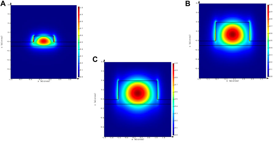
FIGURE 10. Distributions of optical fields of waveguides at (A) 2 μm, (B) 4.3 μm and (C) 5 μm wavelengths.
After the above simulation analysis of the size of the ridge waveguide, it is determined that when the wavelength is 2 μm, Wr = 600 nm, h = 90 nm, H = 220 nm. At 4.3 μm wavelength, Wr = 1500 nm, h = 100 nm, H = 500 nm. At a wavelength of 5 μm, Wr = 1800 nm, h = 100 nm, H = 500 nm. It can be seen from Table 1, when the wavelength is 2 μm, the etching depth of the modulator designed in this paper is 130 nm which is easy to achieve in the preparation process compared to the modulator with an etching depth of 170 nm reported in reference 31. Comparing the device structures operating at wavelengths of 4.3 μm, 5 μm and 3 μm, both Wr and H are smaller than those reported in the reference. The reduction of structure dimensions is conducive to reducing the device area, thereby reducing the power consumption of the device. At the same time, the optical signal can be transmitted with lower loss in our designed waveguide structure by simulation. Moreover, Ws is much smaller than the data of reference, and more carriers can be injected into the waveguide region under the same bias voltage, which is more conducive to the realization of modulation.
According to the above optimized parameters, SiGe/Si PIN heterojunction modulator and Si modulator are simulated, and Figure 11 shows the relationship between the carrier injection concentration and the forward bias voltage of SiGe/Si PIN heterojunction modulator and Si modulator at different working wavelengths. It can be seen from the figure that SiGe/Si PIN heterojunction modulator has a larger carrier injection concentration than Si modulator under the same voltage. When modulation voltage is 2 V, the carrier injection concentration of SiGe/Si PIN heterojunction modulator reach to 1.0e19 cm−3, which is far more than 8.83e18 cm−3 of Si modulator at 2 μm wavelength. According to the change in carrier concentration required for modulation is 1.0e18 cm−3, the modulation voltages of SiGe/Si PIN heterojunction modulator and Si modulator are respectively 0.84 V and 1.71 V at 2 μm wavelength, then the modulated voltage of SiGe/Si PIN heterojunction modulator is lower 50.8% than that of Si modulator under the same modulated effect at 2 μm wavelength; the modulation voltages of SiGe/Si PIN heterojunction modulator and Si modulator are respectively 0.86 V and 1.77 V at 4.3 μm wavelength, then the modulated voltage of SiGe/Si PIN heterojunction modulator is lower 51.4% than that of Si modulator under the same modulated effect at 4.3 μm wavelength; the modulation voltages of SiGe/Si PIN heterojunction modulator and Si modulator are respectively 0.87 V and 1.83 V at 5 μm wavelength, then the modulated voltage of SiGe/Si PIN heterojunction modulator is lower 52.5% than that of Si modulator under the same modulated effect at 5 μm wavelength. As the input optical wavelength continues to increase, the carrier injection concentration is constantly decreasing. From equations (2) and (3), it also can be seen that with the increase of the input optical wavelength, the effective refractive index difference coefficient will continue to decrease, because the carrier injection concentration of waveguide region is decreased with the increase of optical wavelength. Therefore, as shown in Figure 11, under the same voltage, the longer optical wavelength, the lower the carrier injection concentration of SiGe/Si PIN heterojunction modulator, but it is still higher than that of Si modulator.
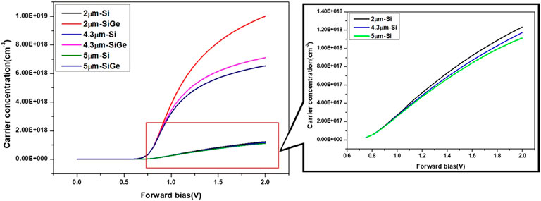
FIGURE 11. Simulation curves of carrier injection concentration and voltage of SiGe/Si PIN heterojunction modulator and Si modulator at different wavelengths.
Based on the above optimization results, the static transmission characterizations of SiGe/Si PIN heterojunction modulator are got. Figure 12A shows the optical transmission spectrum of modulator at 2 μm wavelength. It can be seen from the figure, when the modulation voltage is 0.84 V, the maximum modulation depth of modulator near the center wavelength is 65 dB. At this time, the extinction ratio is 12.81 dB, the insertion loss is 3.4 dB, and the modulation efficiency is about 0.042 Vcm. Figure 12B shows the optical transmission spectrum of modulator at the wavelength of 4.3 μm. At the modulation voltage of 0.86 V, the maximum modulation depth of modulator near the center wavelength is 52 dB. At 4.3 μm wavelength, the extinction ratio is 12.36 dB, and the insertion loss is 3.02 dB. The modulation efficiency is about 0.043 Vcm. Figure 12C shows the optical transmission spectrum of the modulator at a wavelength of 5 μm. When the wavelength of modulator is 5 μm wavelength, the modulation voltage is 0.87 V, and the modulator has a maximum modulation depth of 50 dB near the center wavelength. The extinction ratio of the modulator is 12.22 dB, the insertion loss is 3.0 dB, and the modulation efficiency is about 0.0435 Vcm. The results show that SiGe/Si PIN heterojunction modulator has good static modulation characteristics and the absorption loss of SiO2 is eliminated in the MIR.
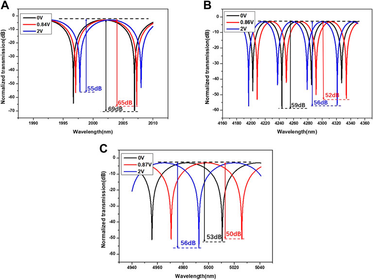
FIGURE 12. Transmission spectra of SiGe/Si PIN heterojunction modulator at (A) 2 μm, (B) 4.3 μm and (C) 5 μm wavelengths.
The high-speed transmission characteristics of SiGe/Si PIN heterojunction modulator under ideal conditions are simulated. Figure 13A–C, show the eye diagram of SiGe/Si PIN heterojunction modulator are at 40 Gbps with CW input signals for 2 μm, 4.3 μm and 5 μm wavelengths, respectively. It can be seen from the figure, the eye diagram can be presented very well at 40 Gbps modulation rate. When the modulation voltage is 0.84 V, the dynamic extinction ratio of SiGe/Si PIN heterojunction modulator is 8.86 dB at 2 μm wavelength; When the modulation voltage is 0.86 V, the dynamic extinction ratio of SiGe/Si PIN heterojunction modulator is 1.17 dB at 4.3 μm wavelength; When the modulation voltage is 0.87 V, the dynamic extinction ratio of SiGe/Si PIN heterojunction modulator is 4.91 dB at 5 μm wavelength. The results show that SiGe/Si PIN heterojunction modulator has good high-speed modulation characteristics and achieve the modulation rate of 40 Gbps in the MIR.
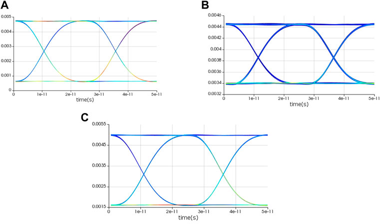
FIGURE 13. Optical eye diagrams of SiGe/Si PIN heterojunction modulator at 40 Gbps for (A) 2 μm, (B) 4.3 μm and (C) 5 μm wavelengths.
Table 2 compares the performance of the modulator between this work and other work of the references. It can be seen from the table that the modulator of this work can achieve a transmission rate of 40 Gbps, and the modulation efficiency of the modulator is significantly better than that reported in reference 34; compared with the modulation depth of the modulator reported in the reference, the SiGe heterojunction modulator of this paper can achieve a modulation depth of up to 65 dB. Especially at the operating wavelength of 2 μm, the extinction ratio of the SiGe heterojunction MZ modulator is close to the result reported in reference 29, but the modulation depth is better.
We introduce a SiGe/Si PIN heterojunction modulator with punch structure based on plasma-dispersion-effect, which can operate at three wavelengths: 2 μm, 4.3 μm and 5 μm. We plan to study the traveling wave electrode and the high-speed characteristics of the modulator in the next work. Based on the theoretical analysis, the electrical and optical characteristics of modulator are simulated, and the structural parameters are optimized. An excellent SiGe/Si heterojunction electro-optic modulator is obtained in the MIR. The SiGe/Si heterojunction electro-optic modulator has the maximum modulation depth of 65 dB, the extinction ratio of 12.81 dB, the dynamic extinction ratio of 8.86 dB, and the modulation efficiency of 0.042 Vcm at 2 μm wavelength; when the working wavelength is 4.3 μm, the modulation depth is 52 dB, the extinction ratio is 12.36 dB, the dynamic extinction ratio is 1.17 dB, and the modulation efficiency is 0.043 Vcm; at the wavelength of 5 μm, the modulator has the modulation depth of 50 dB, the extinction ratio is 12.22 dB, the dynamic extinction ratio is 4.91 dB, and the modulation efficiency is 0.0435 Vcm. The modulator can achieve a modulation rate of 40 Gbps at 2 μm, 4.3 μm and 5 μm wavelengths. At the same time, the SiGe/Si heterojunction modulator has the smallest insertion loss at 5 μm wavelength, which is about 3 dB. SiGe/Si PIN heterojunction modulator with punch structure has good static and high-speed modulation characteristics, the absorption loss of SiO2 is eliminated and the modulation rate of 40 Gbps is achieved in the MIR. This modulator provides a solution for MIR communications in the future.
The original contributions presented in the study are included in the article/supplementary material, further inquiries can be directed to the corresponding author.
SF is the corresponding author and the first author of this paper, XH and SF contributed equally to the work.
This research was funded by National Key Research and Development Program of China (Grant No. 2018YFB2200500), National Natural Science Foundation of China (Grant Nos. 61204080), National Key Laboratory Fund Project (Grant Nos. SKL201804), Key Research and Development Program of Shaanxi Province of China (Grant Nos. 2022GY-012, 2020KW-011), Science and Technology Plan Project of Xi’an (Grant Nos. 2020KJRC0026).
We would like to thank school colleague's help and the support from the government.
The authors declare that the research was conducted in the absence of any commercial or financial relationships that could be construed as a potential conflict of interest.
All claims expressed in this article are solely those of the authors and do not necessarily represent those of their affiliated organizations, or those of the publisher, the editors and the reviewers. Any product that may be evaluated in this article, or claim that may be made by its manufacturer, is not guaranteed or endorsed by the publisher.
1. Soref R. Group IV photonics for the mid infrared. Proc Spie Int Soc Opt Eng (2013) 8629:02. doi:10.1117/12.2013769
2. Tittel FK, Richter D, Fried A. Mid-infrared laser applications in spectroscopy. Top Appl Phys (2003) 89:458–529. doi:10.1007/3-540-36491-9_11
3. Willer U, Saraji M, Khorsandi A, Geiser P, Schade W. Near- and mid-infrared laser monitoring of industrial processes, environment and security applications. Opt Lasers Eng (2006) 44(7):699–710. doi:10.1016/j.optlaseng.2005.04.015
4. Werle P, Slemr F, Maurer K, Kormann R, Muecke R, Jaenker B. Near- and mid-infrared laser-optical sensors for gas analysis. Opt Lasers Eng (2002) 37(2/3):101–14. doi:10.1016/S0143-8166(01)00092-6
5. Sieger M, Mizaikoff B. Toward on-chip mid-infrared sensors. Anal Chem (2016) 88(11):5562–73. doi:10.1021/acs.analchem.5b04143
6. Hattasan N, Kuyken B, Leo F, Ryckeboer M. Vermeulen D. High-efficiency SOI fiber-to-chip grating couplers and low-loss waveguides for the short-wave infrared. Photonics Technology letters. IEEE (2012) 24(17):1536–8. doi:10.1109/LPT.2012.2208452
7. Rouifed MS, Littlejohns CG, Guo XT, Qiu H, Hu T, Zhang Z, et al. Low loss SOI waveguides and MMIs at the MIR wavelength of 2μm. IEEE Photon Tech Lett (2016) 28(24):2827–9. doi:10.1109/LPT.2016.2623319
8. Miller SA, Yu M, Ji X, Griffith AG, Jaime C, Gaeta AL. Low-loss silicon platform for broadband mid-infrared photonics, Optica, 4 (2017). p. 707–12. doi:10.1364/OPTICA.4.000707
9. Dong B, Guo X, Ho CP, Li B, Wang H, Lee C, et al. Silicon-on-Insulator waveguide devices for broadband mid-infrared photonics. IEEE Photon J (2017) 9(3):1–10. doi:10.1109/JPHOT.2017.2692039
10. Fang Q, Chen X, Zhao Y, Hu J, Chen H, Chao Q, et al. Folded silicon-photonics arrayed waveguide grating integrated with loop-mirror reflectors. IEEE Photon J (2018) 10(4):1–8. doi:10.1109/JPHOT.2018.2843368
11. Hu H, Fang Q, Wang S, Zhang X, Ma X, Gu M, et al. Folded 15-channel arrayed waveguide gratings on silicon nitride platform with loop reflector. Opt Commun (2021) 500:1–8. doi:10.1016/j.optcom.2021.127321
12. Alonso-Ramos C, Nedeljkovic M, Benedikovic D, Penadés JS, Littlejohns CG, Khokhar AZ, et al. Germanium-on-Silicon mid-infrared grating couplers with low-reflectivity inverse taper excitation. Opt Lett (2016) 41(18):4324–7. doi:10.1364/ol.41.004324
13. Radosavljevic S, Kuyken B, Roelkens G. Efficient 52 µm wavelength fiber-to-chip grating couplers for the Ge-on-Si and Ge-on-SOI mid-infrared waveguide platform. Opt Express (2017) 25(16):19034–42. doi:10.1364/OE.25.019034
14. Nedeljkovic M, Penades SJ, Mitchell JC, Khokhar ZA. Surface-grating-coupled low-loss Ge-on-Si rib waveguides and multimode interferometers. IEEE Photon Tech Lett (2015) 27(10):1040–3. doi:10.1109/LPT.2015.2405611
15. Du J, He Z. Thermo-optic tunable silicon arrayed waveguide grating at 2μm wavelength band. IEEE Photon J (2020) 12(4):1–8. doi:10.1109/JPHOT.2020.3001595
16. Zheng J, Xue C. 30 GHz GeSn photodetector on SOI substrate for 2 µm wavelength application. Photon Res (2021) 9(4):494–500. doi:10.1364/PRJ.413453
17. Penades JS, Ortega-Moñux A, Nedeljkovic M, Wangüemert-Pérez JG, Halir R, Khokhar AZ, et al. Suspended silicon mid-infrared waveguide devices with subwavelength grating metamaterial cladding. Opt Express (2016) 24(20):22908–16. doi:10.1364/OE.24.022908
18. Penkov B, Asher W. Silicon-on-sapphire integrated waveguides for the mid-infrared. Opt Express (2010) 18(12):12127–35. doi:10.1364/OE.18.012127
19. Chang YC, Paeder V, Hvozdara L, Hartmann JM, Herzig HP. Low-loss germanium strip waveguides on silicon for the mid-infrared. Opt Lett (2012) 37(14):2883–5. doi:10.1364/OL.37.002883
20. Brun M, Labeye P, Grand G, Hartmann J-M, Boulila F, Carras M, et al. Low loss SiGe graded index waveguides for mid-IR applications. Opt Express (2014) 22(1):508–18. doi:10.1364/OE.22.000508
21. Wang W, Zhang Z, Xin G, Hong W. Mid-infrared (MIR) mach-zehnder silicon modulator at 2m wavelength based on interleaved PN junction. CLEO: Sci Innov (2018) 23:55.
22. Sadiq MU, Zhang H, O'Callaghan J, Roycroft B, Kavanagh N, Thomas K, et al. Gb/s WDM transmission over 1.15-km HC-pbgf using an InP-based mach-zehnder modulator at 2μm. J Lightwave Tech (2015) 34(8):1706–11. doi:10.1109/JLT.2015.2508941
23. Nedeljkovic M, Soref R, Mashanovich GZ. Free-Carrier Electrorefraction and Electroabsorption Modulation Predictions for Silicon over the 1&#x2013;14- <formula formulatype=inline><tex Notation=TeX>$\mu\hbox{m}$</tex></formula> Infrared Wavelength Range. IEEE Photon J (2011) 3(6):1171–80. doi:10.1109/JPHOT.2011.2171930
24. Zhou YY. Research on high-speed circuit of silicon-based Mach-Zehnder electro-optical modulator. China: Shanghai Jiao tong University (2014).
25. Soref R, Lorenzo JP. All-silicon active and passive guided-wave components for λ=1.3 and 1.6μm. IEEE J Quan Electron (1986) 22(6):873–9. doi:10.1109/JQE.1986.1073057
26. Brimont A, Gardes FY, Sanchis P, Marris-Morini D, Krauss TF. Eindhoven, Netherlands (2008). p. 321–4.Design of a micro-ring resonator electro-optical modulator embedded in a reverse biased PN junction14th European Conference on Integrated Optics (ECIO 08)
27. Xu SL, Xie MX, Zhang ZP. SiGe microelectronics Technology. Netherlands: National Defense Industry Press (2007).
28. Soref R, Bennett BR. Electrooptical effects in silicon. IEEE J Quan Electron (1987) 23(1):123–9. doi:10.1109/JQE.1987.1073206
29. Hu H, Wang S, Liu Y, Ma X, Gu M. Design of a high extinction ratio silicon optical modulator at 2 µm using the cascaded compensation method. OSA Continuum (2021) 4(7):1933–44. doi:10.1364/OSAC.426592
30. Feng S, Xue B, Li LB, Zhai XJ, Song LX, Zhu CJ. Analysis of Si/SiGe/Si double heterojunction band of a novelstructure of PIN electronic modulation. Acta Phys Sin (2016) 65(05):054201–105. doi:10.7498/aps.65.054201
31. Van Camp MA, Assefa S, Gill DM, Barwicz T, Shank SM, Rice PM, et al. Demonstration of electrooptic modulation at 2165 nm using a silicon Mach-Zehnder interferometer. Opt Express (2012) 20(27):28009–16. doi:10.1364/oe.20.028009
32. Cao W, Nedeljkovic M, Littlejohns CG, Li T, Mashanovich GZ. Silicon and germanium mid-infrared optical modulators. In: Proceedings of the 2018 IEEE Photonics Society Summer Topical Meeting Series (SUM); 09-11 July 2018; Waikoloa, HI, USA. IEEE (2018). doi:10.1109/PHOSST.2018.8456777
33. Li TT, Nedeljkovic M, Hattasan N, Khokhar AZ, Reynolds SA, Stankovic S, et al. Mid-infrared Ge-on-Si electro-absorption modulator. In: Proceedings of the IEEE International Conference on Group IV Photonics; 23-25 August 2017; Berlin, Germany. IEEE (2017). doi:10.1109/GROUP4.2017.8082169
34. Cao W, Thomson DJ, Nedeljkovic M, Alam SU, Rouifed MS. IEEE (2018). doi:10.1109/GROUP4.2018.847869120-Gb/s silicon optical modulators for the 2 μm wavelength bandProceedings of the 2018 IEEE 15th International Conference on Group IV Photonics (GFP)29-31 August 2018Cancun, Mexico
Keywords: electro-optic modulator, SiGe/Si heterojunction, mid-infrared, mach-zehnder modulator, silicon on insulator
Citation: Feng S, Hu X, Feng L, Wang D, Chen M, Liu Y, Hu H and Jia L (2022) The numerical investigations of SiGe/Si heterojunction electro-optic modulator in mid-infrared. Front. Phys. 10:1019113. doi: 10.3389/fphy.2022.1019113
Received: 14 August 2022; Accepted: 26 October 2022;
Published: 07 November 2022.
Edited by:
Chuanbo Li, Minzu University of China, ChinaReviewed by:
Kambiz Abedi, Shahid Beheshti University, IranCopyright © 2022 Feng, Hu, Feng, Wang, Chen, Liu, Hu and Jia. This is an open-access article distributed under the terms of the Creative Commons Attribution License (CC BY). The use, distribution or reproduction in other forums is permitted, provided the original author(s) and the copyright owner(s) are credited and that the original publication in this journal is cited, in accordance with accepted academic practice. No use, distribution or reproduction is permitted which does not comply with these terms.
*Correspondence: Song Feng, ZmVuZ3NvbmdAeHB1LmVkdS5jbg==
Disclaimer: All claims expressed in this article are solely those of the authors and do not necessarily represent those of their affiliated organizations, or those of the publisher, the editors and the reviewers. Any product that may be evaluated in this article or claim that may be made by its manufacturer is not guaranteed or endorsed by the publisher.
Research integrity at Frontiers

Learn more about the work of our research integrity team to safeguard the quality of each article we publish.