
95% of researchers rate our articles as excellent or good
Learn more about the work of our research integrity team to safeguard the quality of each article we publish.
Find out more
ORIGINAL RESEARCH article
Front. Phys. , 21 January 2022
Sec. Optics and Photonics
Volume 9 - 2021 | https://doi.org/10.3389/fphy.2021.814559
This article is part of the Research Topic Advances in Polarimetry and Ellipsometry: Fundamentals and Applications View all 14 articles
 Tim Käseberg1*
 Jana Grundmann1Thomas Siefke2Petr Klapetek3,4
 Miroslav Valtr3,4Stefanie Kroker1,5,6Bernd Bodermann1
Conventional spectroscopic ellipsometry is a powerful tool in optical metrology. However, when it comes to the characterization of non-periodic nanostructures or structured fields that are much smaller than the illumination spot size, it is not well suited as it integrates the results over the whole illuminated area. Instead, imaging ellipsometry can be applied. Especially imaging Mueller matrix ellipsometry is highly useful in nanostructure characterization and defect inspection, as it is capable to measure the complete Mueller matrix for each pixel in a microscope image of the sample. It has been shown that these so-called Mueller matrix images can help to distinguish geometrical features of nanostructures in the sub-wavelength regime due to visible differences in off-diagonal matrix elements. To further investigate the sensitivity of imaging Mueller matrix ellipsometry for sub-wavelength sized features, we designed and fabricated a sample containing geometrical nanostructures with lateral dimensions ranging from 50 to 5,000 nm. The structures consist of square and circular shapes with varying sizes and corner rounding. For the characterization of their Mueller matrix images, we constructed an in-house Mueller matrix microscope capable of measuring the full Mueller matrix for each pixel of a CCD camera, using an imaging system and a dual-rotating compensator configuration for the ellipsometric system. The samples are illuminated at 455 nm wavelength and the measurements can be performed in both transmission and reflection. Using this setup, we systematically examine the sensitivity of Mueller matrix images to small features of the designed nanostructures. Within this contribution, the results are compared with traceable atomic force microscopy measurements and the suitability of this measurement technique in optical nanometrology is discussed. AFM measurements confirm that the fabricated samples closely match their design and are suitable for nanometrological test measurements. Mueller matrix images of the structures show close resemblance to numerical simulations and significant influence of sub-wavelength features to off-diagonal matrix elements.
When it comes to nanostructure characterization via optical metrology, spectroscopic ellipsometry is one of the most powerful and versatile tools available today [1–7]. Especially Mueller matrix ellipsometry, which measures all polarizing properties of the sample under investigation and summarizes them in a 4 by 4 Mueller matrix, is a useful method in layer composition characterization or the retrieval of geometrical parameters of periodic nanostructures [8–10]. As an optical technique, its advantages compared to other methods like atomic force microscopy (AFM) or scanning electron microscopy (SEM) lie in its non-invasive nature, speed, and low setup complexity. However, conventional spectroscopic ellipsometry meets its limits regarding measurements of structured fields smaller than the illumination spot. The measurement signal is usually integrated over the whole illuminated area on the sample. Thus, when the structured fields are inherently smaller than the illumination spot, unwanted signals from the surrounding disturb the measurement signal and lead to distorted results. An additional example where conventional ellipsometry is not well-suited is the measurement of structures that are non-periodic. The integrated Mueller matrix of an individual, non-periodic nanostructure can barely be distinguished from one measured on the substrate alone.
In the cases where conventional ellipsometry does not provide reliable measurement results due to the geometry of the sample, imaging ellipsometry can be used instead. In imaging Mueller matrix ellipsometry, an imaging system is integrated into the analyzing arm of the ellipsometer. This way, the influence of the sample on the polarization is examined spatially and a Mueller matrix for each pixel in an image of the sample is the result. Using such a setup, we can examine the polarizing properties of the sample locally, not limited by the illumination spot size. It is also possible to distinguish different regions of interest in the same measurement that possibly feature different structure characteristics, which makes it also a promising tool for defect inspection measurements [11–20].
The evaluation of Mueller matrix images is usually carried out using the same techniques as in conventional ellipsometry. Measurement results are averaged over homogeneous areas in the images and structural or material parameters are then determined with approximative models by solving the inverse problem [14, 19, 20]. In this paper however, we treat Mueller matrix images with rigorous three-dimensional models of single individual structures instead, by solving the inverse problem from numerically simulating the Mueller matrix images to find relations between nanostructure geometries and measurable effects in off-diagonal elements of the Mueller matrix. For this purpose, we realized an imaging Mueller matrix ellipsometry setup for reflection and transmission measurements at visible wavelengths, which for the first time also features a mode that enables reflection measurements under normal incidence. Thus, the setup combines an imaging Mueller matrix ellipsometer with a Mueller matrix microscope and allows fluid transitions between measurements from angles of incidence ranging between 0° and 90° without laborious reconstructions. Besides our setup, we show and discuss AFM and Mueller matrix measurements on a sample specially designed to test and demonstrate the sensitivity of Mueller matrix images to the form (ranging from circular to square) of individual nanoscale structures. The comparison of measurements and numerical simulations shows clear connections between the shape of nanostructures and their local influence on the Mueller matrix, which can help to reconstruct the non-periodic nanostructures from optical measurements alone. As a potential application for this serves the characterization of the resolution-induced corner rounding present in nanolithographically manufactured structures like semiconductor contact holes with symmetries comparable to the structures examined in this contribution. This paper is organized as follows: In Section 2, a thorough description of our imaging Mueller matrix ellipsometry setup as well as of the samples is given. Section 3 presents the results of the measurements on the samples, followed by a discussion of the results in Section 4. In the end, Section 5 summarizes our results.
Our setup is schematically depicted in Figure 1. The general layout of the setup follows the dual-rotating compensator ellipsometry configuration [21], but with the arms moving in the horizontal plane as can be seen in the photography in Figure 2. A large aperture rotation stage forms the basis of this setup. It is used to rotate the analyzing arm of the ellipsometric system around the sample. The sample is mounted in the middle of the aperture of the large rotation stage on top of a smaller rotation stage and linear adjustment stages. This way, the sample can be rotated independently from the analyzing arm, which allows for measurements at arbitrary sets of incidence and reflection angles.
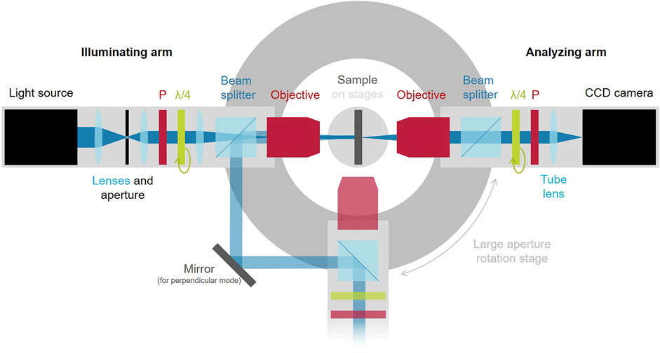
FIGURE 1. Imaging Mueller matrix ellipsometry setup, top view sketch. P: polarizer, λ/4: quarter-wave plate.
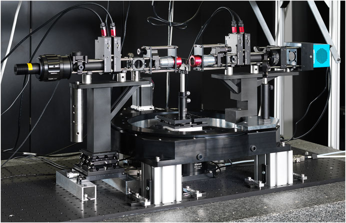
FIGURE 2. Imaging Mueller matrix ellipsometry setup.
The illuminating arm (left side of Figure 2) begins with a light source, which is a blue LED with a center wavelength of 455 nm. The advantage of using monochromatic light with a short wavelength is that a higher resolution in the imaging system can be reached while keeping chromatic aberrations low. For applications at different wavelengths, the LED can be replaced by a white light LED and several filters. The light from the LED is then collected by a large lens, focused onto an aperture and then collimated. The lens system around the aperture serves as a telescope to guide the light through the following optics as well as to emulate a point source for easier collimation. Afterwards, a 90:10 beam splitter plate guides a portion of the light to a powermeter as an intensity reference before it hits the sample. The remaining light then passes a linear Glan-Thompson polarizer (PGT 2.10 from Bernhard Halle Nachfl. GmbH) as well as a superachromatic quarter-wave plate (RSU 1.4.10 from Bernhard Halle Nachfl. GmbH), which together form the polarization state generator. For the measurements shown here, the polarizer is fixed to a horizontal position while the quarter-wave plate is rotated to generate different states of polarization. After passing a 50:50 beam splitter cube (which is used for perpendicular incidence measurements described below), the polarized light is then focused onto the back focal plane of an objective (M Plan Apo NIR B 50x from Mitutoyo). Due to the collimated light being focused on the objective’s entry pupil, the light hitting the sample is mostly collimated again, leading to a homogeneous illumination of the sample in the imaging system. In optical microscopy, this configuration is referred to as Koehler illumination [22, 23]. Contrary to conventional, non-imaging ellipsometry, it is more important to generate a homogeneously illuminated image in this setup than to produce a small focal spot, because the results will be later evaluated for each individual pixel in the image instead of being integrated over the illuminated area.
The analyzing arm mostly mirrors the illuminating arm. It starts with another objective (M Plan Apo NIR B 50x from Mitutoyo) with a working distance of 25.5 mm, a numerical aperture of 0.42 and a ×50 magnification. The long working distance of the objectives allows for the measurement of samples with a diameter of up to 5 cm without restricting the movement of the arms around the sample. This enables a fluent transition between reflection and transmission measurements. In reflection, angles of incidence between 90° and 37.5° can be reached, limited only by the size of the objectives. The polarization state of the light is then analyzed by another set of quarter-wave plate and linear polarizer, which both can again be rotated around the optical axis. Afterwards, a tube lens focuses the light onto the chip of a CCD camera. The camera chip features 2,688 by 2,200 pixels with a size of 4.54 μm by 4.54 μm [24].
Measurement results are presented as 4 by 4 Mueller matrices where each element contains one image with the values of this particular matrix element for each pixel in the image. To show a simple example for how measurements are presented in this contribution, an idealized transmission measurement without sample is shown in Figure 3. The values of the dimensionless matrix elements are color-coded, where red stands for a positive sign and blue represents a negative sign. The Mueller matrix of the free space is just the identity matrix, so all matrix elements in Figure 3 are zero except for those on the main diagonal where they are 1. Figure 3 also contains the common naming for the individual matrix elements, which are usually numbered in the following way:
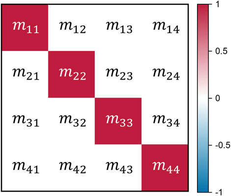
FIGURE 3. Mueller matrix example for a transmission measurement without sample.
For measurements at normal incidence, our setup features a special microscopy mode. In this mode, the analyzing arm is moved to a position in a 90° angle to the illuminating arm and a mirror is placed between the objective and the polarization state analyzer. The setup now resembles the layout of a conventional optical microscope with perpendicular incidence. This is also illustrated in Figure 1 as the transparent beam path. The light reflected from the sample back into the objective of the illuminating arm is then guided by the beam splitter over the mirror and another beam splitter into the analyzing arm. This way, reflection measurements at normal incidence can be carried out without major reconstructions of the system. Additionally, the sample can still be rotated independently for angle corrections or potentially for minor scatterometric applications.
The setup is operated with a standard dual-rotating compensator configuration [21]. During the measurement, the polarizers are fixed to parallel positions for high intensity throughput. The first polarizer imprints a linear polarization on the illumination from the light source while the second polarizer analyzes the state of polarization after interaction with the sample. Meanwhile, the first quarter-wave plate rotates in steps of 5°, and the second quarter-wave plate rotates in steps of 25°, which is a way to create a harmonic modulation of the states of polarization. The modulated intensity measured at each pixel of the CCD camera depends not only on the polarizing optics in the system, but also on the influence of the Mueller matrix of the sample, and can be described as:
where p and a represent the elements of the Stokes vectors resulting from the influence of the optical components in the illuminating and the analyzing arm, respectively, starting from an unpolarized light source. The elements of the Mueller matrix of the sample are described by mij (compare Figure 3), while c is a constant factor for the camera sensitivity [21]. This modulated intensity can be evaluated by a Fourier analysis in each individual pixel of the CCD camera to obtain the Mueller matrix elements mij for each pixel and thus Mueller matrix images [25].
The stepwise movement of the compensators allows for a better control of the measurement as well as a better quality of the measured images in the CCD camera. At each step, several images can be recorded and averaged for a reduction of image noise. This method leads to measurement times of about 7 minutes for a full rotation of the first compensator. Alternatively, a continuous rotation mode where the movement of the retarders is synchronized with the frame rate of the camera is possible to speed up the measurement at the expense of image quality. The evalutation of the Mueller matrix images is performed using a custom built Python program.
For systematic tests on the influence of the form and symmetry of nanostructures on off-diagonal Mueller matrix elements, we designed and fabricated a sample consisting of individual structures written into a 100 nm thick layer of polymethylmethacrylat (PMMA) on a 100 mm diameter silicon wafer using electron beam lithography. The structures are placed in the middle of 5 mm by 5 mm sized fields on the sample to prevent interactions between different structures and to leave enough room for the illumination spot of the measurement system to only illuminate one structure at a time. An overview of the sample is depicted in Figure 4. The fields are organized in rows, labeled from A to D, for different structure types and in columns, labeled from 1 to 10, for different feature sizes. Row A contains square structures with 5 μm width and height and varying corner radii between 100 nm and 2 μm, resulting in a transition from nearly perfect square to nearly perfect circle. Rows B and C contain square and circular structures, respectively, ranging in diameter from 50 nm to 2 μm. Row D contains small arrays of 1 μm sized squares with 10 and 20 μm pitch and up to 4 by 4 squares per array. For a more detailed list of the sample parameters, Table 1. Previously, a test wafer has been produced and characterized concerning the feature size fabrication accuracy using SEM [26].
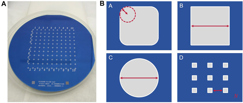
FIGURE 4. Overview of the sample with nanoform structures. (A) Wafer with columns and rows. Structure parameters are varied over the columns. (B) Sketches of the structures in the different rows. Red arrows highlight which parameters are varied. (i): Corner rounding of fixed size squares. (ii): Size of squares. (iii): Size of circles. (iv): Pitch and number (N) of structures in a small array.
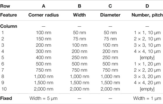
TABLE 1. Sample design feature parameter overview.
For an elaborated evaluation of ellipsometric measurements, the solution of the inverse problem is usually needed. In this course, a model of the examined structures is built and then fitted to the measurement results to retrieve information like layer thicknesses, structure geometries, or material parameters. However, in the case of imaging ellipsometry on non-periodic structures, their simulation is inherently more complex than for simple layer structures, periodic structures, or in non-imaging ellipsometry. The reason for this is the need for three-dimensional models of the structure itself which take significantly higher computational costs compared to the periodic two-dimensional models in conventional ellipsometry or the layer-stack models usually used in imaging ellipsometry [4, 27]. Only by modelling the nanostructures in three dimensions, the local influence of the geometric parameters of non-periodic nanostructures on the Mueller matrix can correctly be accounted for. Additionally, for a correct reconstruction of the Mueller matrix images measured with an imaging system, the simulation of microscope images with a defined illumination would be needed. This includes the superposition of many simulations at different pupil points inside the numerical aperture of the light illuminating the sample. In doing so, a high number of pupil points is as important as their distribution inside the numerical aperture, and both affect the computational costs of solving the inverse problem as a whole [28, 29].
For this reason, we modelled the structures on the sample using the finite element method (FEM) Maxwell solver JCMsuite [30] based only on the target values for a qualitative comparison. The illumination was simulated using only one pupil point, which corresponds to a plane wave illumination, at 455 nm wavelength under perpendicular incidence. Using mesh sizes of up to 500 nm and finite element degrees up to 5, computational costs for the simulation of one structure included about 350 GB RAM and about 2 h of computation time.
The structures in row A on the sample feature 5 μm by 5 μm sized square structures with different corner radii. We measured the Mueller matrix images of these structures at our setup, using the perpendicular incidence microscopy mode. As an example, Figure 5A) shows the results for structures A1, A5, and A10. For comparison, the structures of row A on the sample were also simulated using FEM. The resulting Mueller matrix images for the structures A1, A5, and A10 are presented in Figure 5C). Images and results of the remaining structures can be found in the supplement.
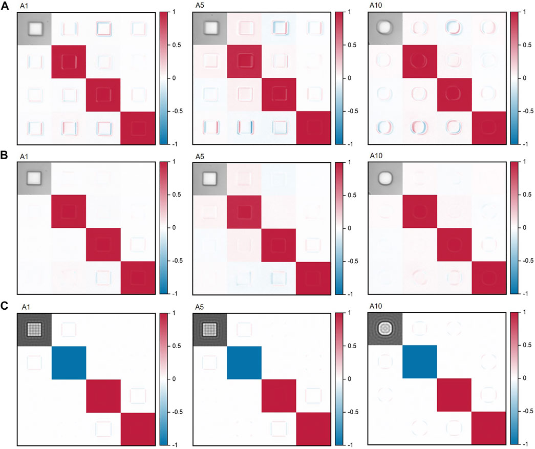
FIGURE 5. Mueller matrix images of structures A1, A5, and A10, (A) not corrected for thermal drift, (B) corrected for thermal drift, and (C) simulated. Target feature sizes: 5 μm width and height, corner radii: 100 nm (A1), 400 nm (A5), 2000 nm (A10).
The square and circular structures in rows B and C range in size from 50 nm to 2 μm. To test the resolution of our setup, we measured Mueller matrix images of the circular structures in row C. As square structures tend to degenerate into circular ones for very small structure sizes due to the fabrication process, we focused on the evaluation of the circular structures first. Figure 6 shows the measured Mueller matrix images of the structures C6 and C10 as an example.
FIGURE 6. Mueller matrix images of structures C6 and C10 not corrected for thermal drift. Target feature sizes: 500 nm width (C6) and 2000 nm width (C10).
For comparison with the measurements at our imaging Mueller matrix ellipsometry setup, we performed measurements using a metrological scanning probe microscope (SPM) [31] and a commercial AFM with a high aspect ratio probe that was calibrated using the metrological SPM and a transfer standard. The scan size and resolution were adapted to the feature size, typically using 1,024 by 1,024 pixels per image. The data was processed in the open-source software Gwyddion [32].
For row A, the structures A1, A5, A6, and A10 were measured. Measurements on the structures in row A were evaluated using the Gwyddion function “Fit shape” and using a parametric model for a hole with round corners. Measured images are shown in Figure 7 and an example of the fitted shape difference from the measured data is shown in Figure 8. Measured feature sizes are summarized in Table 2. The measurement uncertainty was estimated to be 20 nm. The uncertainty estimations given here are based on the typical uncertainties of the microscopes, repeatability, and estimates of the major uncertainty influences during the measurement (fast axis direction, feedback loop effects, tip convolution, drift, fit error). The biggest contribution is the tip shape, which affects nearly all the measurements on smaller spots, as can be also seen from the images.
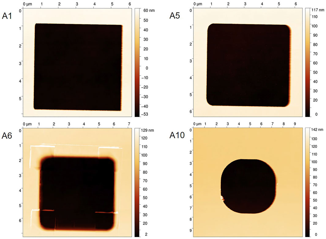
FIGURE 7. AFM measurements of structures in row A.
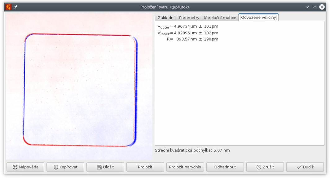
FIGURE 8. Example for fitted shape difference of AFM measurements.
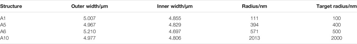
TABLE 2. Feature sizes of structures in row A, measured by AFM.
Measurements of the structures B4, B6, C4, C6, D4, and D9 are shown in Figure 9. Results for the structures are collected in Table 3. The uncertainty is predominantly influenced by the tip radius. This component was estimated to be 13 nm for width measurements and 30 nm for pitch measurements.
FIGURE 9. AFM measurements of structures (A) B4 and B6, (B) C4 and C6, and (C) D4 and D9 with (D) details of single squares.

TABLE 3. Feature sizes of structures in row B, C, and D, measured by AFM.
The sizes of the nanoform structures were characterized using traceable AFM. For row A, the structures A1, A5, A6, and A10 were examined. The measured outer widths deviate on average by 1.4% from the fabrication target value of 5 μm. The measured corner radii of these structures deviate from the design by 6.8% on average. Width and corner radius deviation are largely influenced by partial resist damage in structure A6 as visible in Figure 7. For the structures in row B and C, the measured feature sizes deviate on average by 8 nm from the design, which is smaller than the estimated measurement uncertainty of 13 nm due to the tip shape. The pitches of the structures measured in row D match the design with a deviation of 14 nm for D4 and 22 nm for D9, which is smaller than the uncertainty estimation for pitch measurements of 30 nm for D4 and 61 nm for D9. The size of the structures varies only by 0.4% nm on average. All in all, the fabricated structures on the sample closely match the design and can be used for further nanoform characterization measurements.
Mueller matrix image measurements on the structures A1, A5, and A10 are depicted in Figure 5A). As usual, the Mueller matrix elements are all normalized to the first element m11 in the upper left corner, except for this element itself, as it mostly represents the overall measured intensity. The measurements were performed in the perpendicular incidence mode, so the light passed a couple of mirrors on its way to the camera. For this reason, the Mueller matrix images look like transmission measurements, with all main diagonal elements being positive comparable to Figure 3, although the light was measured in reflection from the sample. Furthermore, the images were normalized to a reference measurement on the substrate that was taken right after the measurement of the structure to eliminate polarizing effects from the optical elements as well as influences from the substrate itself. The first elements of each Mueller matrix show a certain blur that also reappears in the other matrix elements. This blur is most likely caused by thermal drift of the sample during the measurement. It is accounted for by a drift correction algorithm: In each image of a measurement series, the structure under investigation is detected and the image then recentered to the center of mass of the structure. This way, we obtained the drift corrected Mueller matrix images presented in Figure 5B) for the structures A1, A5, and A10. A more detailed view of selected images is given in Figure 10.
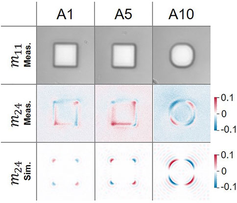
FIGURE 10. Selected Mueller matrix images of structures A1, A5, and A10: Measured m11 element and measured and simulated m24 elements. Measurement results from drift corrected measurements.
The drift corrected Mueller matrix images show distinct polarization effects at the edges of the structures. These effects would not be measurable in conventional, non-imaging ellipsometry. The effects visible in the uncorrected images are noticeably more pronounced, but are also mostly caused by the thermal drift of the structure. However, the edge effects that are left after the drift correction are inherently local polarization effects caused by the sample. This is confirmed by the simulation results depicted in Figure 5C). The simulation results represent idealized measurement results, because for the simulation, the design target values where used and the illumination was assumed to be a perfect plane wave from only one pupil point. During measurements with the setup in perpendicular incidence mode, the light that was reflected from the sample back into the first objective is guided to the analyzing system by several mirrors. In this course, each reflection changes the sign of some of the Mueller matrix elements. Because of this, the measured Mueller matrix looks like a transmission measurement. However, the simulation does not take these mirrors into account. Therefore, some simulated Mueller matrix elements have the opposite sign compared to the measurements, which is most prominent in the m22 element. Nevertheless, even without an optimization of the geometrical parameters towards the measured values or using a more elaborate model of the illumination, the local polarization effects visible at the edges and corners of the structures closely resemble the ones observed in the drift corrected measurements, indicating a successful suppression of the drift effect from the correction algorithm.
Concerning their metrological use, the off-diagonal Mueller matrix images deliver additional information channels for structure form characterization exceeding optical microscopy alone. In Figure 10, the Mueller matrix elements m11 and m24 of the measurements as well as m24 of the simulations of the structures A1, A5, and A10 are visualized with color bars adjusted to the range of only these elements. Although the m11 elements of structures A1 and A5 are visibly indistinguishable, the off-diagonal matrix elements show clear indications on the changing corner rounding from 100 to 400 nm. Especially in element m24, the change is evident from the absolute value of the matrix element in the corners changing by 15% in the measurements and 85% in the simulations. The change from A5 to A10 is with about 160% in both measurements and simulations even more pronounced. Other off-diagonal matrix elements, like m42, m13 and m31, also show increasing absolute values in the corners or on the edges of the structures with an increased corner radius. Thus, local geometry features like the orientation of an edge or the curvature of a corner do have significant connections to the sign and value of the local Mueller matrix, even for changes below the wavelength of the illumination, which can be exploited for example by fitting an appropriate three-dimensional model to the structure to solve the inverse problem and retrieving the structural parameters.
The measurements on the smaller structures in rows B and C were also affected by the thermal drift discussed earlier, as can be seen from the example measurements in Figure 6 on C6 and C10. However, the drift correction algorithm was not able to reliably recognize these structures because of their small size. Therefore, these measurements could not be corrected yet and no meaningful comparison with simulated results would be possible on the uncorrected images. Thus, no clear indications about the resolution limits of our measurement technique could be gained by now. However, the visible difference in off-diagonal matrix elements for structures A1 and A5 with corner radii 100 and 400 nm, respectively, promises a possible distinction of feature sizes well below the wavelength of the system.
In this contribution, we presented our imaging Mueller matrix ellipsometry setup which we constructed and tested on specially designed nanostructures to further investigate in the link between geometrical features and off-diagonal Mueller matrix elements. Our setup has a horizontal positioning of the analyzing ellipsometer arm, enabling us to perform measurements in transmission as well as reflection at arbitrary angle combinations in the visible wavelength regime. Therefore, reflection measurements can be performed between 37.5° and 90° angles of incidence. Additionally, our setup features a microscopy mode that allows for reflection measurements at perpendicular incidence without major reconstructions of the setup. To examine the influence of the form of nanostructures on Mueller matrix elements, we designed and fabricated a collection of structures with simple geometrical shapes and sizes ranging from 50 nm to 5 μm. Traceable AFM measurements showed that the fabricated samples closely match the design, with average size deviations of 2.1% and average corner radius deviations of 6.8%. These deviations can partially be explained by the finite tip shape of the AFM, but are most likely due to fabrication tolerances. The overall small deviation from the design makes the structures suitable for further nanometrological test measurements. We measured structures of the rows A and C using our Mueller matrix microscopy setup. Due to thermal drifts of the sample, the smaller structures in row C could not be evaluated meaningfully. For the larger structures in row A, a drift correction algorithm was successfully implemented and the resulting corrected Mueller matrix images compared to FEM simulations of the design structures. Even without fitting the simulations to the measurements, we could observe a close resemblance of the measurements to the simulations. Furthermore, the measurements as well as the simulations showed a significant influence of a change in the corner radius of the structures from 100 to 400 nm on off-diagonal Mueller matrix elements, most prominently m24 and m42. This reinforces the potential of imaging Mueller matrix ellipsometry in metrological applications towards the characterization of sub-wavelength sized nanostructures.
The original contributions presented in the study are included in the article/Supplementary Material, further inquiries can be directed to the corresponding author.
TK: Performing Mueller matrix ellipsometry measurements, code writing, discussing results, writing the paper. JG: Code writing, performing Mueller matrix ellipsometry measurements. TS: Sample fabrication and preparation. PK and MV: Performing AFM measurements and discussing results. SK and BB: Discussing results and writing the paper.
This work is funded through the project 17FUN01 “BeCOMe” within the Programme EMPIR. The EMPIR initiative is co-founded by the European Union’s Horizon 2020 research and innovation program and the EMPIR Participating Countries. This project (20FUN02 “POLight”) has received funding from the EMPIR programme co-financed by the Participating States and from the European Union’s Horizon 2020 research and innovation programme. SK also acknowledges partial support by the Deutsche Forschungsgemeinschaft (DFG, German Research Foundation) under Germanys Excellence Strategy—EXC-2123 QuantumFrontiers—390 837 967.
The authors declare that the research was conducted in the absence of any commercial or financial relationships that could be construed as a potential conflict of interest.
All claims expressed in this article are solely those of the authors and do not necessarily represent those of their affiliated organizations, or those of the publisher, the editors and the reviewers. Any product that may be evaluated in this article, or claim that may be made by its manufacturer, is not guaranteed or endorsed by the publisher.
The Supplementary Material for this article can be found online at: https://www.frontiersin.org/articles/10.3389/fphy.2021.814559/full#supplementary-material
1. Rothen A The Ellipsometer, an Apparatus to Measure Thicknesses of Thin Surface Films. Rev Scientific Instr (1945) 16:26–30. doi:10.1063/1.1770315
2. Vedam K Spectroscopic Ellipsometry: a Historical Overview. Thin Solid Films (1998) 313-314:1–9. doi:10.1016/s0040-6090(97)00762-1
3. Losurdo M Applications of Ellipsometry in Nanoscale Science: Needs, Status, Achievements and Future Challenges. Thin Solid Films (2011) 519:2575–83. doi:10.1016/j.tsf.2010.11.066
5. Chen X, Liu S, Zhang C, Jiang H, Ma Z, Sun T, et al. Accurate Characterization of Nanoimprinted Resist Patterns Using Mueller Matrix Ellipsometry. Opt Express (2014) 22:15165–77. doi:10.1364/OE.22.015165
6. Liu S, Chen X, Zhang C Development of a Broadband Mueller Matrix Ellipsometer as a Powerful Tool for Nanostructure Metrology. Thin Solid Films (2015) 584:176–85. doi:10.1016/j.tsf.2015.02.006
7. Rossow U A Brief History of Ellipsometry. Phys Status Solidi B (2019) 256:1800307. doi:10.1002/pssb.201800307
8. Azzam R. Mueller-matrix Ellipsometry: a Review. Spie-int Soc Opt Eng (1997) 3121:396–405. doi:10.1117/12.283870
9. Dixit D, Keller N, Lifshitz Y, Kagalwala T, Elia A, Todi V, et al. Nonconventional Applications of Mueller Matrix-Based Scatterometry for Advanced Technology Nodes. J Micro/Nanolithography, MEMS, MOEMS (2018) 17:034001. doi:10.1117/1.jmm.17.3.034001
10. Voloshenko I, Gompf B, Berrier A, Dressel M, Schnoering G, Rommel M, et al. Mueller Matrix Metrology: Depolarization Reveals Size Distribution. Appl Phys Lett (2019) 115:063106. doi:10.1063/1.5094409
11. Chipman RA, Pezzaniti JL. Imaging Ellipsometry of Optical Coatings In Situ. In: Optical Thin Films IV: New Developments, Vol. 2262. Bellingham, Washington, USA: International Society for Optics and Photonics (1994). p. 124–34.
12. Jin G, Jansson R, Arwin H Imaging Ellipsometry Revisited: Developments for Visualization of Thin Transparent Layers on Silicon Substrates. Rev Scientific Instr (1996) 67:2930–6. doi:10.1063/1.1147074
13. Kerwien N Zum Einfluss von Polarisationseffekten in der mikroskopischen Bildentstehung. Stuttgart, Germany: Universität Stuttgart (2007). doi:10.18419/opus-4130
14. Asinovski L, Beaglehole D, Clarkson MT Imaging Ellipsometry: Quantitative Analysis. Phys Stat Sol (A) (2008) 205:764–71. doi:10.1002/pssa.200777855
15. Mujat M, Iftimia N, Ferguson D, Hammer D. Mueller Matrix Microscopy. In: Biomedical Optics. Washington, D.C., USA: Optical Society of America (2010). p. BSuD60.
16. Liu S, Du W, Chen X, Jiang H, Zhang C Mueller Matrix Imaging Ellipsometry for Nanostructure Metrology. Opt Express (2015) 23:17316–29. doi:10.1364/OE.23.017316
17. Chandel S, Soni J, Ray SK, Das A, Ghosh A, Raj S, et al. Complete Polarization Characterization of Single Plasmonic Nanoparticle Enabled by a Novel Dark-Field Mueller Matrix Spectroscopy System. Sci Rep (2016) 6:26466–10. doi:10.1038/srep26466
18. Tan Y, Chen C, Chen X, Du W, Gu H, Liu S Development of a Tomographic Mueller-Matrix Scatterometer for Nanostructure Metrology. Rev Scientific Instr (2018) 89:073702. doi:10.1063/1.5034440
19. Duwe M, Quast J-H, Schneider S, Fischer D, Beck U Thin-film Metrology of Tilted and Curved Surfaces by Imaging Mueller-Matrix Ellipsometry. J Vacuum Sci Technol B (2019) 37:062908. doi:10.1116/1.5122757
20. Wang C, Chen X, Chen C, Sheng S, Song L, Gu H, et al. Reconstruction of Finite Deep Sub-wavelength Nanostructures by Mueller-Matrix Scattered-Field Microscopy. Opt Express (2021) 29:32158–68. doi:10.1364/oe.432611
21. Azzam RMA Photopolarimetric Measurement of the Mueller Matrix by Fourier Analysis of a Single Detected Signal. Opt Lett (1978) 2:148–50. doi:10.1364/OL.2.000148
22. Köhler A. Ein neues Beleuchtungsverfahren für mikrophotographische Zwecke. Z für wissenschaftliche Mikroskopie für Mikroskopische Technik (1893) 10:433–40.
23. Gross H. Handbook of Optical Systems, Volume 1, Fundamentals of Technical Optics. Weinheim, Germany: Wiley VCH (2005).
24. Grundmann J. Konzeption und Realisierung eines experimentellen Müller-Matrix-Mikroskop-Aufbaus. Master Thesis. Braunschweig: PTB (2020).
26. Käseberg T, Dickmann J, Siefke T, Wurm M, Kroker S, Bodermann B Mueller Matrix Ellipsometry for Enhanced Optical Form Metrology of Sub-lambda Structures. In: B Bodermann, K Frenner, and RM Silver, editors. Modeling Aspects in Optical Metrology VII. International Society for Optics and Photonics (SPIE), Vol. 11057. Bellingham, Washington, USA: SPIE (2019). p. 155–65. doi:10.1117/12.2527419
27. Liu J, Zhang D, Yu D, Ren M, Xu J. Machine Learning Powered Ellipsometry. Light: Sci Appl (2021) 10:1–7. doi:10.1038/s41377-021-00482-0
28. Förster S, Gross H, Höller F, Höring L, Extended Depth of Focus as a Process of Pupil Manipulation. Opt Des Eng (2005) 5962:596207. doi:10.1117/12.624814
29. Lu X, Gross H Efficient Simulation of Surface Scattering in Symmetry-free Optical Systems. Opt Express (2020) 28:39368–86. doi:10.1364/oe.411028
31. Lazar J, Klapetek P, Valtr M, Hrabina J, Buchta Z, Cip O, et al. Short-range Six-axis Interferometer Controlled Positioning for Scanning Probe Microscopy. Sensors (2014) 14:877–86. doi:10.3390/s140100877
Keywords: metrology, nanometrology, ellipsometry, mueller ellipsometry, imaging ellipsometry, nanostructures, mueller matrix ellipsometry
Citation: Käseberg T, Grundmann J, Siefke T, Klapetek P, Valtr M, Kroker S and Bodermann B (2022) Mueller Matrix Ellipsometric Approach on the Imaging of Sub-Wavelength Nanostructures. Front. Phys. 9:814559. doi: 10.3389/fphy.2021.814559
Received: 13 November 2021; Accepted: 16 December 2021;
Published: 21 January 2022.
Edited by:
Hao Jiang, Huazhong University of Science and Technology, ChinaReviewed by:
Alpan Bek, Middle East Technical University, TurkeyCopyright © 2022 Käseberg, Grundmann, Siefke, Klapetek, Valtr, Kroker and Bodermann. This is an open-access article distributed under the terms of the Creative Commons Attribution License (CC BY). The use, distribution or reproduction in other forums is permitted, provided the original author(s) and the copyright owner(s) are credited and that the original publication in this journal is cited, in accordance with accepted academic practice. No use, distribution or reproduction is permitted which does not comply with these terms.
*Correspondence: Tim Käseberg, dGltLmthZXNlYmVyZ0BwdGIuZGU=
Disclaimer: All claims expressed in this article are solely those of the authors and do not necessarily represent those of their affiliated organizations, or those of the publisher, the editors and the reviewers. Any product that may be evaluated in this article or claim that may be made by its manufacturer is not guaranteed or endorsed by the publisher.
Research integrity at Frontiers
Learn more about the work of our research integrity team to safeguard the quality of each article we publish.