 Weiming Xiong
 Weijin Chen
 Yue Zheng1,2
- 1State Key Laboratory of Optoelectronic Materials and Technologies, School of Physics, Sun Yat-sen University, Guangzhou, China
- 2Centre for Physical Mechanics and Biophysics, School of Physics, Sun Yat-sen University, Guangzhou, China
- 3School of Materials, Sun Yat-sen University, Guangzhou, China
Ferroelectric vortex has attracted much attention as a promising candidate for memories with high density and high stability. It is a crucial problem to precisely manipulate the vortex chirality in order to utilize it to store information. Nevertheless, so far, a practical and direct strategy for vortex switching is still lacking. Moreover, the strong coupling of chirality between neighboring vortices in continuous systems like superlattices limits the application of ferroelectric-vortex-based memories. Here, we design a ferroelectric nanoplate junction to break the strong coupling between neighboring vortices. Phase-field simulation results demonstrate that the vortex chirality of the nanoplates could be efficiently tuned by sweeping local electric and thermal fields in the nanoplate junction. More importantly, the weak coupling between two neighboring nanoplates through the intermediate junction brings a deterministic vortex switching behavior. Based on this, we propose a concept of vortex memory devices. Our study provides an effective way to control the vortex chirality and suggests an opportunity for designing new memory devices based on ferroelectric vortex.
Introduction
Ferroelectric vortex, the toroidal arrangement of electrical dipoles in ferroelectrics, has attracted much attention over the past decades in both theoretical and experimental studies due to their wonderful properties different from the conventional polar domain structures [1–5]. Generally, two degenerate chiral states of vortex, i.e., clockwise (CW) and counterclockwise (CCW), could form stably in the low-dimensional ferroelectric systems. It is a natural idea to utilize the two distinguished states to carry information, e.g., CW vortex denotes the information “0” and CCW vortex denotes the information “1.” Importantly, the vortex is a topological structure that possesses a strong stability property and small size (typically a few nanometers in diameter), holding promise in developing a new type of ferroelectric memory device with high stability and density (∼10 Tb/inch2).
Since ferroelectric vortex was predicted in ferroelectric nanodisks and nanorods via a first-principles-derived effective Hamiltonian [1], a large number of theoretical and experimental studies were carried out to gain further understanding of the structure [2–8]. Toward the applications of vortex-based memories, one of the concerning issues is the deterministic manipulation of vortex chirality. Since the toroidal moment of a ferroelectric vortex is conjugated to a curled electric field, the chirality of a ferroelectric vortex could be switched by a curled electric field, which has been demonstrated based on the phase field method and effective Hamiltonian method [6–8]. Nevertheless, it is still a challenge in practice to realize a large enough and highly localized curled electric field to switch the vortex [9–18]. To avoid the use of curled electric fields, various vortex switching strategies have been also proposed, e.g., via geometry design [9–12], defect engineering [13, 14], asymmetric mechanical loads [14–16], nonuniform electric fields [17], sweeping tip fields [18], etc. The key idea of these strategies is to bring some kind of asymmetry to the vortex system, such that nucleation of vortex with a deterministic charity is favored. For instance, Chen et al. [14] introduced an asymmetric mechanical field, e.g., caused by local clamping force or dislocations, to break the spatial symmetry of the ferroelectric vortex in nanodots. Consequently, the vortex is easily switched by a homogeneous electric field. Ma et al. [18] exploited a sweeping biased tip to break the time symmetry of annihilation and nucleation dynamics of the ferroelectric vortex. As a result, the vortex could be efficiently switched by such a sweeping tip-induced local electric field in a “dynamic switching” mode.
Despite several advanced strategies have been proposed to realize the switching of vortex, a practical and direct method, which aims to get rid of requirements on the sample and harsh technologies, is still lacking. On the other aspect, neighboring vortices in continuous systems like superlattices are strongly coupled and always have opposite chirality to minimize the domain wall and electrostatic energies of the system (as shown schematically in Figure 1A). This means that the information of the vortex array cannot be individually stored and manipulated. This property limits the design and application of vortex-based memories. Therefore, it is necessary to break the coupling between two neighboring vortices.
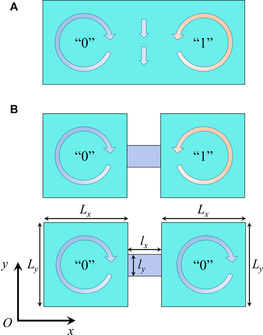
FIGURE 1. (A) Schematic illustration of information stored by a double-vortices state in a rectangular nanoplate. Chiralities of two vortices are coupled with each other and always opposite. The vortices with counterclockwise and clockwise chirality carry the information “1” and “0,” respectively. (B) Schematic illustration of information stored in a nanoplate junction. Chiralities of the two neighboring vortices are weakly coupled, enabling the storage of different information (e.g., “0” and “1”) and similar information (e.g., “0” and “0”).
In this work, we design a nanoplate junction system that consist of two nanoplates and one junction region (Figure 1B). The two nanoplates have the same geometry (i.e., Lx and Ly along x and y directions, respectively), and the junction region has the lateral sizes of lx and ly, with lx(y)<Lx(y). It is expected that, in such a nanoplate junction, the chiralities of two neighboring vortices become weakly coupled with each other. The neighboring vortices in the nanoplate junction not only can carry different information (i.e., “1” and “0” or “0” and “1”), but also can carry similar information (i.e., “0” and “0” or “1” and “1”), hence enabling a two-bit memory element. More importantly, due to presence of an intermediate junction region, this two nanoplates are weakly coupled such that the vortex chirality could be switched more easily than that in the individual nanoplate. To demonstrate the above scenario, phase field simulations are performed to reveal the vortex formation and switching dynamics in nanoplate junctions of different geometries. Moreover, we construct nanoplate junction arrays in conjunction with a s region and show that the information carried by the vortices can be readily controlled by sweeping local electric and thermal fields. Our results thus demonstrate an efficient strategy to manipulate the chirality of ferroelectric vortex and suggest an alternative possibility of developing ferroelectric-vortex-based memory devices.
Methods
Phase Field Model
In this work, a phase field model is established to capture the vortex formation and switching dynamics in ferroelectric nanoplate junctions. In this model, the spontaneous polarization field P=(P1, P2, P3) is chosen as order parameter field, whose temporal evolution can be described by the time-dependent Ginzburg-Landau (TDGL) equation,
Where F is the total free energy of the system, M is kinetic parameter related to the polarization switching dynamics and t is time.
For ferroelectric nanosystems, the total free energy is described by the sum of bulk free energies and a surface free energy,
Where fLand, felas, fgrad, felec and fsurf are the energy densities of the Landau free energy, elastic energy, gradient energy, electrostatic energy and surface energy, respectively. Pi,j, εij, and Ei are the gradients of polarization, the components of the strain and electric field, respectively.
For perovskite ferroelectrics like PbTiO3 (PTO), the Landau free energy density fLand is given by the form of a six-order polynomial [19, 20],
With αi, αij, αijk and αijkl being the thermodynamic coefficients of the Landau free energy. Here, α1 is temperature-dependent and is expressed as
The eigenstrain
With cijkl being the elastic stiffness tensor and
The gradient energy density fgrad induced by the gradient of polarization is given by a form in a second-order approximation of Taylor expansion,
Where gijkl are the gradient energy coefficients.
Based on the concept of background dielectric constant, the electrostatic energy density felec is given by,
Where
The relaxation of local spontaneous polarization near the surface contributes to the surface energy. Based on the concept of extrapolation length, the surface energy density fsurf can be modeled by the following simple form [23],
Where
In this simulation, the nanoplate junctions are modeled to be made of PTO. Two-dimensional (2D) discrete grids are employed with grid spacings both being 1 nm along the lateral x and y directions. It is worthy to notice that the tetragonal vortex state prefers to form in the tetragonal PTO nanoplate. Therefore, the 2D model can capture the features and its evolution of the vortex state in ferroelectrics at suitable conditions. To have a good control of the vortex switching, nanofilm regions with a polar-domain state are also included in the system in the demo of vortex array memory devices. Periodic boundary conditions are applied along the y direction in the nanofilm region. The evolution of polarization is solved numerically by discretizing the TDGL equation in time. At each time step, the strain and electric fields are obtained by solving the mechanical and electrostatic equilibrium equations with the appropriate boundary conditions. Values of the material coefficients [20, 22, 25, 26] used in the simulation are listed in the Table 1.
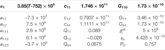
TABLE 1. Values of parameters in simulations (SI units and T in K).
Finite Element Method
In the phase-field simulations, strain and electric fields are solved by the finite element method. According to variation relationship, the mechanical and electrostatic equilibrium equations (Eqs 4, 6) can be solved by looking for the extreme value of following functionals, i.e.,
Where the displacement ui and the electric potential φ are employed as the freedoms of the functionals. Then, these two equations could be rewritten into the matrix form, i.e.,
For 2D model, vectors and matrices are defined as,
In the simulations, the ferroelectric is meshed into four-node cubic elements. After denoting the displacement vector and the electric potential at the ith nodes of an element as
Then, the displacement and the electric potential in the element are given by,
With
Where Nui and Nφi are the interpolation functions.
In the next step, the Eq. 12 is substituted into Eq. 9. In order to find out the extreme value of these two functionals, and the variation of two functionals with respect to the
Here, e and
With
Here,
Where {U} and {Φ} are the vectors containing all the node displacement and electric potential, respectively. Then, the node displacement and electric potential could be obtained by solving the Eq. 17 via the Gauss-Seidel iteration method.
Results and Discussions
Domain Formation in Nanoplate Junction
First of all, we have an insight into the effect of geometry of the junction region on the formation of vortices in the nanoplate junction. In the nanoplate junction, the Lx and Ly of the nanoplates are both set to be 10 nm, lx of the junction region is set to be 4 nm, and ly varies in the range of 8–2 nm. For the nanoplate junctions with different ly, various random polarization perturbations are employed as initial inputs to the vortex formation at room temperature, zero external electric field and strain under the open-circuit condition. After evolution according to the TDGL equations, two kinds of vortex states (i.e., vortices in the two nanoplates have similar or opposite chiralities) can be stabilized in the nanoplate junctions. In Figure 2, the left panels show the vortex states with similar dipole rotation in the two nanoplates of nanoplate junctions under different ly. When ly is equal to 8 and 6 nm, as respectively shown in Figures 2A,B, only one vortex forms in the nanoplate junction. These results are similar to the vortex state with one vortex in the PTO nanoplate in previous works [14, 15]. When ly decreases to 4 nm (Figure 2C), two complete vortices could be stably formed in the two nanoplates. In this case, a vortex also forms in the junction region and the polarization magnitude is about half of the magnitude in the two nanoplates. More importantly, the vortices of two nanoplates are coupled with the junction region and could be affected by the vortex state of the junction region. If ly decreases to 2 nm (Figure 2D), the junction region is almost paraelectric. The coupling between the two vortices in the nanoplates becomes even weaker. Moreover, vortices with opposite toroidal arrangements of the dipoles in two nanoplates are also found, as shown in the right panels in Figure 2. For cases ly equal to 8 and 6 nm, the polarization in the junction region is strongly coupled with one of the nanoplates and the nanoplate and the junction region together form a vortex. When ly decreases to 4 and 2 nm, two complete vortices with opposite chiralities could be stably formed in the two nanoplates. Consistent with the previous results, the polarization magnitude is about half of the magnitude in the nanoplates when ly = 4 nm while the polarization in the junction region is almost zero when ly = 2 nm.
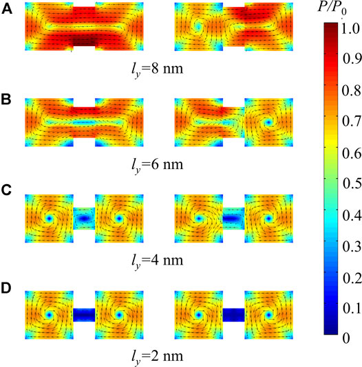
FIGURE 2. Formation of vortex states in the nanoplate junctions with different ly, (A) 8 nm, (B) 6 nm, (C) 4 nm, (D) 2 nm. Random polarization perturbations are employed as initial inputs to the vortex formation at room temperature, zero external electric field and strain under the open-circuit condition. After evolution, two kinds of vortex states (i.e., vortices in the two nanoplates have similar or opposite chiralities) can be stabilized in the nanoplate junctions as respectively shown in the left and right panels.
Controllability of Vortex Chirality Under a Sweeping Local Electric Field
Based on the vortex states in the nanoplate junctions, ly is chosen as 4 nm to ensure the independence of two vortices in the two nanoplates. Meanwhile, the chiralities of these two vortices could interact with each other through the polarization in the junction region. In the following, a nanoplate-junction array with five nanoplates in conjunction with a polar-domain nanofilm region is constructed to demo the deterministic switching of vortex chirality and the possibility of developing a new kind of vortex-based memory device. We first consider the vortex switching induced by a sweeping local electric field. The initial information carried by the vortex array is set to be (0, 1, 0, 1, 1), as shown in Figure 3. The local electric field is applied to the system with a profile
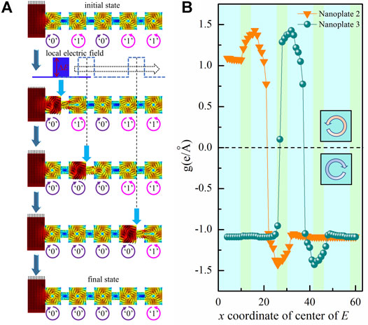
FIGURE 3. (A) Demo of deterministic vortex switching in a nanoplate-junction array with five nanoplates in conjunction with a polar-domain nanofilm region under a sweeping local electric field. The sweeping local electric field is directed along the y axis and sweeping along x axis with a sweeping step of 1 nm. The initial information (0, 1, 0, 1, 1) is rewritten to (0, 0, 0, 0, 1) in the final state after applying a sweeping local electric field. (B) The corresponding evolution of toroidization g of the second and third nanoplates (labeled as Nanoplate 2 and Nanoplate 3, respectively) under the sweeping local electric field. The x axis respects the position of the center of local field E.
Controllability of Vortex Chirality Under a Sweeping Local Thermal Field
Furthermore, we carried out another stimulus, i.e., a sweeping local thermal field, to explore the controllability of vortex chirality in a nanoplate-junction array with five nanoplates in conjunction with a polar-domain nanofilm region. Such a local thermal field could be practically realized by a laser spot. At the beginning, the nanoplate array is set to carry the information of (0, 1, 0, 1, 1). In the simulations, the center of the local heat source is swept from the nanoplate-nanofilm interface with a sweeping step of 1 nm. The distribution of the temperature field is assumed to be a Gaussian shape, i.e.,
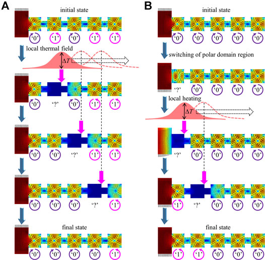
FIGURE 4. Deterministic vortex switching in a nanoplate-junction array with five nanoplates in conjunction with an (A) upward or (B) downward polar-domain nanofilm region under a sweeping local thermal field. In the simulations, the center of the local heat source is swept from the nanoplate-nanofilm interface with a sweeping step of 1 nm. The distribution of the temperature field is assumed to be a Gaussian shape.
From the above simulations, it is clear to see that the vortex chirality of a nanoplate bit can be switched to be the same as the neighboring nanoplate (either the left or the right nanoplate depending on the sweeping direction). This is to say, if a local electric or thermal field sweeps above a nanoplate-junction array from left to right (or reversely), all the bits swept across by the field would be finally in the same state with the leftmost (right most) bit. How can we switch the vortices if all vortices have the same chirality? It is noteworthy that as demonstrated in previous work [12], the chirality of the vortex can be alternated by switching the polarization of the nanofilm right below in a PTO nanofilm-nanodot system. Based on this finding, one can make use of a nanofilm region with a polar domain to control the vortex chirality of the first nanoplate of the nanoplate array. We take the case of vortex switching under a sweeping local thermal field as an example, as shown in Figure 4B. After reversing the polarization direction of nanofilm region, a local heat source is swept from the nanoplate-nanofilm interface to the edge of the first nanoplate. When the local thermal field is removed, we find that the vortex chirality is switched from CW to CCW. The initial information “0” is rewritten to the information “1.” Furthermore, the local heat source is swept to the edge of the second nanoplate and a vortex switching from CW (“0”) to CCW (“1”) is observed. Therefore, the bidirectional switching of the vortex state has been demonstrated in ferroelectric nanoplate junction system.
Discussion
The above path-dependent vortex switching behaviors under the sweeping local electric and thermal fields therefore indicate new memory device concepts based on the weak coupling of ferroelectric vortices in nanoplate junction systems, as schematically shown in Figure 5. Figure 5A depicts a vortex-array memory device controlled by a sweeping local electric field. The nanoplates with vortices of different chiralities are employed to carry the information. Local electric field is applied through two sets of electrodes, i.e., electrode 1 and electrode 2. By selectively applying the bias voltages (i.e., Vin+ and Vin−) to electrodes, a local electric field is applied to a specific nanoplate to manipulate the vortex chirality of the nanoplate. Meanwhile, a nanofilm region with polar domain is also included in the device to reset the information. Similarly, we can also design a vortex-array memory device controlled by a sweeping local thermal field, as shown in Figure 5B. For this device, the laser could be used to provide a local heat source. With the sweeping of laser-induced local thermal field, the vortex chirality of nanoplates could be controlled in a feasible way.
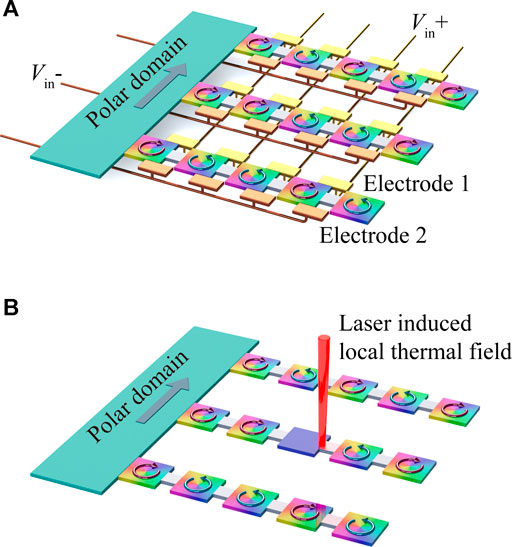
FIGURE 5. Schematics of new memory device concepts based on the weak coupling of ferroelectric vortices in nanoplate junction systems. (A) A vortex-array memory device controlled by a sweeping local electric field. (B) A vortex-array memory device controlled by a sweeping local thermal field.
Conclusions
In conclusion, we propose a ferroelectric nanoplate junction structure to break the strong coupling between neighboring vortices such that vortex-based memory devices which enable independent information storage and feasible vortex switching scheme can be realized. Via phase field simulations, we first study the vortex formation in the nanoplate junction with various geometries of the junction region. It shows that when the junction region is small enough, the vortex chiralities of two neighboring nanoplates in the nanoplate junction become almost independent. Meanwhile, the vortices of two nanoplates weakly interact with each other through the polarization field in the junction region. Due to due to presence of the intermediate junction region, the chirality of the vortex in a nanoplate can be deterministically switched via a sweeping local electric or thermal field. This work proposes an efficient and practical strategy to manipulate the chirality of ferroelectric vortex and suggests an opportunity for designing the memory devices based on ferroelectric vortex.
Data Availability Statement
The raw data supporting the conclusions of this article will be made available by the authors, without undue reservation.
Author Contributions
WC and YZ conceived the research. WX, WC, and YZ designed, performed and analyzed the modeling, WX and WC wrote the manuscript. All authors discussed the results, commented on the manuscript and approved it for publication.
Funding
This work was supported by the National Natural Science Foundation of China (Grants 12072380 and 11702335) to WX, by the National Natural Science Foundation of China (Grant 11972382) to WC, by the National Natural Science Foundation of China (Grant 12132020) to YZ, and by the National Natural Science Foundation of China (Grant 11832019) to Biao Wang, by the Guangzhou Science and Technology Project (Grant 2019060001) to YZ. The simulations reported were performed on resources provided by the National Supercomputer Center in Guangzhou and the Rosamond Computation Center in School of Physics at Sun Yat-sen University.
Conflict of Interest
The authors declare that the research was conducted in the absence of any commercial or financial relationships that could be construed as a potential conflict of interest.
Publisher’s Note
All claims expressed in this article are solely those of the authors and do not necessarily represent those of their affiliated organizations, or those of the publisher, the editors and the reviewers. Any product that may be evaluated in this article, or claim that may be made by its manufacturer, is not guaranteed or endorsed by the publisher.
References
1. Naumov II, Bellaiche L, Fu H. Unusual Phase Transitions in Ferroelectric Nanodisks and Nanorods. Nature (2004) 432:737–40. doi:10.1038/nature03107
2. Zheng Y, Chen WJ. Characteristics and Controllability of Vortices in Ferromagnetics, Ferroelectrics, and Multiferroics. Rep Prog Phys (2017) 80:086501. doi:10.1088/1361-6633/aa5e03
3. Tang YL, Zhu YL, Ma XL, Borisevich AY, Morozovska AN, Eliseev EA, et al. Observation of a Periodic Array of Flux-Closure Quadrants in Strained Ferroelectric PbTiO 3 Films. Science (2015) 348:547–51. doi:10.1126/science.1259869
4. Yadav AK, Nelson CT, Hsu SL, Hong Z, Clarkson JD, Schlepütz CM, et al. Observation of Polar Vortices in Oxide Superlattices. Nature (2016) 530:198–201. doi:10.1038/nature16463
5. Tian G, Yang W, Chen D, Fan Z, Hou Z, Alexe M, et al. Topological Domain States and Magnetoelectric Properties in Multiferroic Nanostructures. Natl Sci Rev (2019) 6(4):684–702. doi:10.1093/nsr/nwz100
6. Naumov II, Fu H. Cooperative Response ofPb(ZrTi)O3Nanoparticles to Curled Electric Fields. Phys Rev Lett (2008) 101:197601. doi:10.1103/PhysRevLett.101.197601
7. Wang J, Kamlah M. Intrinsic Switching of Polarization Vortex in Ferroelectric Nanotubes. Phys Rev B (2009) 80:012101. doi:10.1103/PhysRevB.80.012101
8. Wang J. Switching Mechanism of Polarization Vortex in Single-crystal Ferroelectric Nanodots. Appl Phys Lett (2010) 97:192901. doi:10.1063/1.3515847
9. Van Lich L, Shimada T, Wang J, Dinh V-H, Bui TQ, Kitamura T. Switching the Chirality of a Ferroelectric Vortex in Designed Nanostructures by a Homogeneous Electric Field. Phys Rev B (2017) 96:134119. doi:10.1103/PhysRevB.96.134119
10. Dinh-Van H, Lich LV, Bui TQ, Le TV, Nguyen T-G, Shimada T, et al. Intrinsic and Extrinsic Effects on the Electrotoroidic Switching in a Ferroelectric Notched Nanodot by a Homogeneous Electric Field. Phys Chem Chem Phys (2019) 21:25011–22. doi:10.1039/C9CP04676C
11. Van Lich L, Le M-T, Vu N-L, Nguyen H-D, Le V-T, Ha M-T, et al. Direct Switching of Polarization Vortex in Triangular Ferroelectric Nanodots: Role of Crystal Orientation. Phys Rev B (2021) 104:024104. doi:10.1103/PhysRevB.104.024104
12. Chen WJ, Zheng Y, Wang B, Liu JY. Coexistence of Toroidal and Polar Domains in Ferroelectric Systems: A Strategy for Switching Ferroelectric Vortex. J Appl Phys (2014) 115:214106. doi:10.1063/1.4881530
13. Yuan S, Chen WJ, Ma LL, Ji Y, Xiong WM, Liu JY, et al. Defect-mediated Vortex Multiplication and Annihilation in Ferroelectrics and the Feasibility of Vortex Switching by Stress. Acta Materialia (2018) 148:330–43. doi:10.1016/j.actamat.2018.01.018
14. Chen WJ, Zheng Y. Vortex Switching in Ferroelectric Nanodots and its Feasibility by a Homogeneous Electric Field: Effects of Substrate, Dislocations and Local Clamping Force. Acta Materialia (2015) 88:41–54. doi:10.1016/j.actamat.2015.01.041
15. Chen WJ, Zheng Y, Wang B. Vortex Domain Structure in Ferroelectric Nanoplatelets and Control of its Transformation by Mechanical Load. Sci Rep (2012) 2:00796. doi:10.1038/srep00796
16. Chen WJ, Zheng Y, Wang B. Phase Field Simulations of Stress Controlling the Vortex Domain Structures in Ferroelectric Nanosheets. Appl Phys Lett (2012) 100:062901. doi:10.1063/1.3681379
17. Prosandeev S, Ponomareva I, Kornev I, Naumov I, Bellaiche L. Controlling Toroidal Moment by Means of an Inhomogeneous Static Field: AnAb Initio Study. Phys Rev Lett (2006) 96:237601. doi:10.1103/PhysRevLett.96.237601
18. Ma LL, Ji Y, Chen WJ, Liu JY, Liu YL, Wang B, et al. Direct Electrical Switching of Ferroelectric Vortices by a Sweeping Biased Tip. Acta Materialia (2018) 158:23–37. doi:10.1016/j.actamat.2018.07.024
19. Haun MJ, Furman E, Jang SJ, McKinstry HA, Cross LE. Thermodynamic Theory of PbTiO3. J Appl Phys (1987) 62:3331–8. doi:10.1063/1.339293
20. Pertsev NA, Zembilgotov AG, Tagantsev AK. Effect of Mechanical Boundary Conditions on Phase Diagrams of Epitaxial Ferroelectric Thin Films. Phys Rev Lett (1998) 80:1988–91. doi:10.1103/PhysRevLett.80.1988
21. Tagantsev AK. Landau Expansion for Ferroelectrics: Which Variable to Use. Ferroelectrics (2008) 375:19–27. doi:10.1080/00150190802437746
22. Zheng Y, Woo CH. Thermodynamic Modeling of Critical Properties of Ferroelectric Superlattices in Nano-Scale. Appl Phys A (2009) 97:617–26. doi:10.1007/s00339-009-5261-8
23. Kretschmer R, Binder K. Surface Effects on Phase Transitions in Ferroelectrics and Dipolar Magnets. Phys Rev B (1979) 20:1065–76. doi:10.1103/PhysRevB.20.1065
24. Fu H, Bellaiche L. Ferroelectricity in Barium Titanate Quantum Dots and Wires. Phys Rev Lett (2003) 91:257601. doi:10.1103/PhysRevLett.91.257601
25. Ishikawa K, Uemori T. Surface Relaxation in Ferroelectric Perovskites. Phys Rev B (1999) 60:11841–5. doi:10.1103/PhysRevB.60.11841
Keywords: ferroelectric, vortex, memory, switching, phase field
Citation: Xiong W, Chen W and Zheng Y (2022) Path-dependent Vortex Switching in Ferroelectric Nanoplate Junctions Toward a Memory Device Concept. Front. Phys. 9:791019. doi: 10.3389/fphy.2021.791019
Received: 07 October 2021; Accepted: 22 December 2021;
Published: 14 January 2022.
Edited by:
Ranjith Ramadurai, Indian Institute of Technology Hyderabad, IndiaReviewed by:
Saswata Bhattacharya, Indian Institute of Technology Hyderabad, IndiaKhian-Hooi Chew, University of Malaya, Malaysia
Copyright © 2022 Xiong, Chen and Zheng. This is an open-access article distributed under the terms of the Creative Commons Attribution License (CC BY). The use, distribution or reproduction in other forums is permitted, provided the original author(s) and the copyright owner(s) are credited and that the original publication in this journal is cited, in accordance with accepted academic practice. No use, distribution or reproduction is permitted which does not comply with these terms.
*Correspondence: Weijin Chen, chenweijin@mail.sysu.edu.cn