- 1School of Vehicle Engineering, Xi’an Aeronautical University, Xi’an, China
- 2Department of Communications Engineering, Tohoku University, Sendai, Japan
- 3School of Information and Communications Engineering, Xi’an Jiaotong University, Xi’an, China
- 4Microsystem and Terahertz Research Center, China Academy of Engineering Physics, Chengdu, China
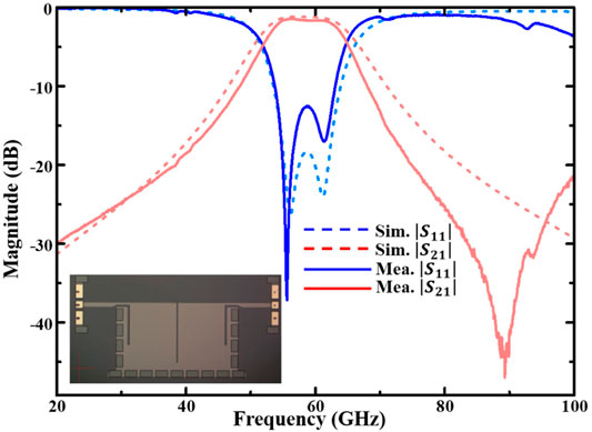
A compact 60-GHz on-chip bandpass filter (BPF) is presented using gallium arsenide (GaAs) technology. The miniaturization is achieved by the half-mode substrate-integrated waveguide (HMSIW) structure. Finally, a prototype of the BPF is fabricated and tested to validate the proposed idea, whose simulated and measured results are in good agreement. The measurements show that it has a center frequency at 58.6 GHz with a bandwidth of 17.9%, and the minimum insertion loss within the passband is 1.2 dB. The chip, excluding the feedings, is only about 0.38
Introduction
Recent developments in semiconductor technology have enabled the pursuit of miniaturized applications based on on-chip millimeter-wave (mmW) devices and systems to become popular, such as automotive mmW radar. The on-chip bandpass filter (BPF) design for millimeter-wave transceivers has, thus, attracted more attention and has made numerous breakthroughs. Abundant investigations have been oriented based on the conventional silicon-based semiconductor technology–integrated circuit process (e.g., CMOS, SiGe, etc.) pursuing low cost with compact physical occupation [1–9]. But meanwhile, the low loss of BPF is also very demanding. The Gallium arsenide (GaAs) process is a desirable candidate for lower in-band insertion loss and higher steep edge with high-operating frequency. Consequently, some works on GaAs–based BPFs have been reported in recent years [10–14]. However, the design of GaAs–based BPFs that consider both size and loss has still not been proposed. In our previous work [13], the proposed BPF achieves bandwidth of over 50% based on the spoof surface plasmon polaritons transmission line theory, but the size is bulky, reaching
Considering compatibility with the integrated circuit system, a BPF based on substrate-integrated waveguide (SIW) technology is introduced with high-Q factor, low loss, and easy fabrication [15]. Furthermore, half-mode SIW (HMSIW) saves about half of the SIW dimension with almost same performance for the design of BPFs. The HMSIW BPF implemented based on GaAs technology is expected to balance the size and loss. However, few BPF works are explored using HMSIW in GaAs technology at the millimeter-wave frequencies.
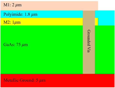
In this article, for the first time, we implement the HMSIW structure based on the GaAs standard process. A compact 60-GHz on-chip BPF is proposed based on HMSIW with the 0.15-
Design Method and Analysis
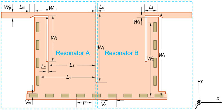
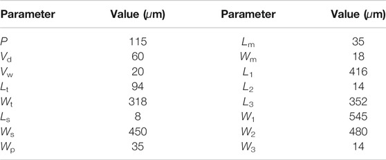
A pair of HMSIW cavity resonators is employed to realize BPF response and miniaturized size. The compact structure is constructed with transition from the microstrip line to HMSIW for further layout size saving. The detailed configuration of the slotted HMSIW BPF is demonstrated in Figure 2, which consists of an input/output microstrip line and slotted HMSIW structure. The HMSIW cavity is divided into two symmetrical cavity resonators, A and B, by the transversal slot. Therefore, each resonator’s boundary is constructed by one electric wall (EW) and three magnetic walls (MWs), as shown in Figure 3A. The EW is formed by rows of metal vias, as the tangential component of the electric field is almost zero near the surface of these via holes. In contrast, the other three side edges are used as MWs because the tangential component of the magnetic field is zero. Therefore, the resonator cavity can be approximately equivalent to a segment of the microstrip line propagating along the x-axis which is open-circuited at one end and short-circuited at the other end. Moreover, the resonator length along x-axis is
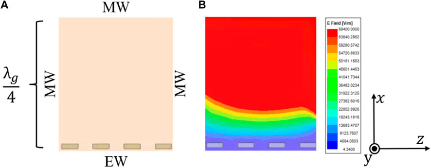
FIGURE 3. (A) HMSIW resonator and (B) electric field distribution of the quasi-TEM mode of the HMSIW resonator.
The standard microstrip propagation mode is the quasi-transversal electromagnetic (TEM) wave. The TEM mode indicates that both the electric field and magnetic field are perpendicular to the direction of electromagnetic wave propagation. In the resonator cavity, the electric field is along y-axis, while the magnetic field is along z-axis. The fields are mostly within the GaAs dielectric of the cavity and partly in the air region adjacent to the edge of the cavity. The phase speed of TEM fields in the GaAs region would be
where W2 is the width of the HMSIW shown in Figure 2.
The mutual coupling between two identical HMSIW resonators A and B is defined as inter-coupling. One more resonant frequency will be generated because of the inter-coupling scheme [24]. Therefore, the resonant frequency fc of the HMSIW cavity will be split into two resonant frequencies, represented by f1 and f2, respectively. Thus, these two frequencies are controlled by the inter-coupling between two HMSIW resonators. The inter-coupling coefficient k can be acquired by simulation from ANSYS HFSS and can be evaluated as [24]:
It can be seen that the coupling coefficient k is proportional to the separation between the resonant frequency points f1 and f2. As a result, the tighter the coupling is, the wider will be the separation of f1 and f2, and the bandwidth of the BPF is thus expanded. On the other hand, the coupling strength can be tuned by changing the length Ls and width Ws of the transversal slot inserted between the two HMSIW cavity resonators. When these values increase, the gap between HMSIW resonators will be increased, and the coupling strength will be reduced, resulting in decreased bandwidth and lower insertion loss. Figure 4 shows the simulated results using the Ansys HFSS simulator to verify the relationships between slot size variation and BPF frequency response. The S-parameters are used to evaluate the electromagnetic (EM) performance. S11 and S21 represent the reflection and transmission coefficients of the EM wave, respectively.
When choosing the final values of Ls and Ws, both bandwidth and loss requirements should be considered to make a balance. Usually, the value of |S11| should be lower than -10 dB in the passband, but the ultra-low |S11| value would result in bandwidth reduction. The value of |S21| represents the insertion loss (IL) within the passband of the filter and the suppression at the stopband. Considering the fringing field effect, the values 8
The external coupling between the HMSIW resonator and input/output feed line can be defined by the external quality factor Qe, and its value can be calculated by the equation [25]:
where τS11 is the group delay of S11 at resonant frequency; f0 is the center frequency of the BPF passband.
In this work, the value of Qe is 7.8 which is extracted by the Ansys HFSS simulator. It can be tuned by changing the dimension of the structure which transfers from the microstrip line to HMSIW. To miniaturize the overall size, direct connection is proposed instead of the traditional gradual changing structure. The corresponding impedance matching can be performed by the slot between the feeding port and HMSIW. The length of the slot is Wt, while the width is L2. Therefore, the values of |S11| and |S21| can be also adjusted by Wt and L2, as shown in Figure 5. As discussed before, the |S11| is suggested to be about −17 dB, and the center frequency should be near 60 GHz. Consequently, Wt and L2 are selected as 300
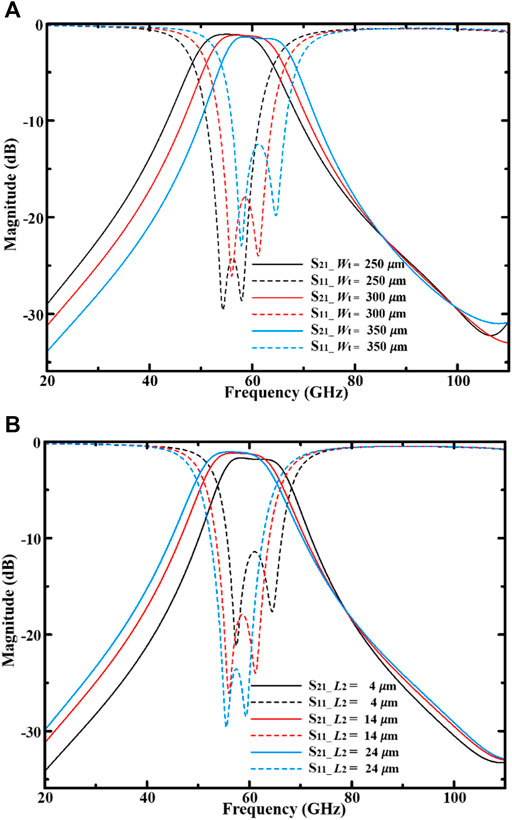
FIGURE 5. S-parameters of the HMSIW BPF with (A) varied Wt at L2 = 14
Results
The prototype of the designed HMSIW BPF filter is fabricated as shown in the inset of Figure 6. The overall size excluding two Ground–Signal–Ground (GSG) pads is
Table 2 shows the characteristic comparisons with some other reported SIW/HMSIW BPFs. The results demonstrate that both IL and size of our proposed HMSIW filter are better than those of the SIW filter in [11] using the same GaAs technology. Compared with our previous work [14], the IL of 1.2 dB has been improved. The IL of the filter using LTCC in [23] is lower than the proposed work, but its size is bulky, increased by more than 6 times. Moreover, the solution in [23] is not too easy to integrate with other active devices which require to be designed on the same wafer.
Conclusion
The bandwidth and insertion loss of the passband can be easily tuned by adjusting the dimension of the slot between the two HMSIW cavity resonators. The center frequency can be evaluated by the single HMSIW resonator. The direct connection structure is deployed for the transition from the microstrip line to HMSIW considering size saving. The fabricated BPF prototype centered at 58.6 GHz has a broadband filtering response with very good insertion loss and return loss. The measurement results agree well with the simulation results. The HMSIW and compact feeding configuration for the design of the BPF are useful to improve the circuit occupation on the chip. At the same time, performance has been not deteriorated compared with other traditional SIW/HMSIW BPFs. It also illustrates that the energy leakage, bandgap effect, etc. of the HMSIW with the period square vias in the GaAs process is also applicable. Owing to these virtues, the proposed HMSIW BPF can be easily integrated with other GaAs components and circuits in mmW systems such as vehicle-mounted radar and 5G communications.
Data Availability Statement
The original contributions presented in the study are included in the article/Supplementary Material; further inquiries can be directed to the corresponding author
Author Contributions
X-JL and WW contributed to this work equally. All authors listed have made a substantial, direct, and intellectual contribution to the work and approved it for publication.
Funding
This work was supported in part by the NSAF Joint Fund under Grant U2130102, in part by the Natural Science Foundation of Shaanxi Province under Grant 2021JQ-060, and in part by the “Siyuan Scholar” Fellowship of XJTU.
Conflict of Interest
The authors declare that the research was conducted in the absence of any commercial or financial relationships that could be construed as a potential conflict of interest.
Publisher’s Note
All claims expressed in this article are solely those of the authors and do not necessarily represent those of their affiliated organizations, or those of the publisher, the editors, and the reviewers. Any product that may be evaluated in this article, or claim that may be made by its manufacturer, is not guaranteed or endorsed by the publisher.
References
1. HsuCheng-Ying C, ChuangHuey-Ru C, Chuang H. A 60-GHz Millimeter-Wave Bandpass Filter Using 0.18-μm CMOS Technology. IEEE Electron Device Lett (2008) 29(3):246–8. doi:10.1109/LED.2007.915369
2. Franc A-L, Pistono E, Gloria D, Ferrari P. High-Performance Shielded Coplanar Waveguides for the Design of CMOS 60-GHz Bandpass Filters. IEEE Trans Electron Devices (2012) 59(5):1219–26. doi:10.1109/TED.2012.2186301
3. Yang Y, Liu H, Hou ZJ, Zhu X, Dutkiewicz E, Xue Q. Compact On-Chip Bandpass Filter with Improved In-Band Flatness and Stopband Attenuation in 0.13-μm (Bi)-CMOS Technology. IEEE Electron Device Lett (2017) 38(10):1359–62. doi:10.1109/LED.2017.2739186
4. El-Hameed ASA, Barakat A, Abdel-Rahman AB, Allam A, Pokharel RK. Ultracompact 60-GHz CMOS BPF Employing Broadside-Coupled Open-Loop Resonators. IEEE Microw Wireless Compon Lett (2017) 27(9):818–20. doi:10.1109/LMWC.2017.2734771
5. Zhu H, Yang Y, Zhu X, Sun Y, Wong S-W. Miniaturized Resonator and Bandpass Filter for Silicon-Based Monolithic Microwave and Millimeter-Wave Integrated Circuits. IEEE Trans Circuits Syst (2018) 65(12):4062–71. doi:10.1109/TCSI.2018.2839701
6. Li M, Yang Y, Xu KD, Zhu X, Wong SW. Microwave On-Chip Bandpass Filter Based on Hybrid Coupling Technique. IEEE Trans Electron Devices (2018) 65(12):5453–9. doi:10.1109/TED.2018.2876324
7. Luo C, Wong SW, Chen RS, Zhu X, Yang Y, Lin JY, et al. Compact On-Chip Millimetre Wave Bandpass Filters with Meandered Grounding Resonator in 0.13-μm (Bi)-CMOS Technology. IET Microwaves, Antennas & Propagation (2020) 14(6):559–65. doi:10.1049/iet-map.2019.0192
8. Xu K-D, Zhu X, Yang Y, Chen Q. A Broadband On-Chip Bandpass Filter Using Shunt Dual-Layer Meander-Line Resonators. IEEE Electron Device Lett (2020) 41(11):1617–20. doi:10.1109/LED.2020.3027734
9. Ge Z, Chen L, Yang L, Gómez-García R, Zhu X. On-Chip Millimeter-Wave Integrated Absorptive Bandstop Filter in (Bi)-CMOS Technology. IEEE Electron Device Lett (2021) 42(1):114–7. doi:10.1109/LED.2020.3036036
10. Li L-P, Shen W, Ding J-Y, Sun X-W. Compact 60-GHz On-Chip Bandpass Filter with Low Insertion Loss. IEEE Electron Device Lett (2018) 39(1):12–4. doi:10.1109/LED.2017.2778714
11. Xiao Y, Shan P, Zhao Y, Sun H, Yang F. Design of a $W$ -Band GaAs-Based SIW Chip Filter Using Higher Order Mode Resonances. IEEE Microw Wireless Compon Lett (2019) 29(2):104–6. doi:10.1109/LMWC.2018.2890265
12. Guo Y-J, Xu K-D, Deng X, Cheng X, Chen Q. Millimeter-Wave On-Chip Bandpass Filter Based on Spoof Surface Plasmon Polaritons. IEEE Electron Device Lett (2020) 41(8):1165–8. doi:10.1109/LED.2020.3003804
13. Xu K-D, Guo Y-J, Yang Q, Zhang Y-L, Deng X, Zhang A, et al. On-Chip GaAs-Based Spoof Surface Plasmon Polaritons at Millimeter-Wave Regime. IEEE Photon Technol Lett (2021) 33(5):255–8. doi:10.1109/LPT.2021.3054962
14. Xu K-D, Guo Y-J, Liu Y, Deng X, Chen Q, Ma Z. 60-GHz Compact Dual-Mode On-Chip Bandpass Filter Using GaAs Technology. IEEE Electron Device Lett (2021) 42(8):1120–3. doi:10.1109/LED.2021.3091277
15. Hong W, Liu B, Wang Y, Lai Q, Tang H, Yin XX, et al. Half Mode Substrate Integrated Waveguide: A New Guided Wave Structure for Microwave and Millimeter Wave Application. In: 2006 Joint 31st International Conference on Infrared Millimeter Waves and 14th International Conference on Teraherz Electronics; 2006 Sept 18-22; Shanghai, China (2006), p. 219. doi:10.1109/ICIMW.2006.368427
16. Zhou S, Wang Z, Xu R, Shen D, Zhan M. A Novel X-Band Half Mode Substrate Integrated Waveguide (HMSIW) Bandpass Filter. In: 2009 Asia Pacific Microwave Conference; 2009 Dec 7-10; Singapore (2009), p. 1387–9. doi:10.1109/APMC.2009.5384496
17. Wang Y, Hong W, Dong Y, Liu B, Tang HJ, Chen J, et al. Half Mode Substrate Integrated Waveguide (HMSIW) Bandpass Filter. IEEE Microw Wireless Compon Lett (2007) 17(4):265–7. doi:10.1109/LMWC.2007.892958
18. Zhang Q-L, Wang B-Z, Zhao D-S, Wu K. A Compact Half-Mode Substrate Integrated Waveguide Bandpass Filter with Wide Out-Of-Band Rejection. IEEE Microw Wireless Compon Lett (2016) 26(7):501–3. doi:10.1109/LMWC.2016.2574997
19. Jones TR, Daneshmand M. Miniaturized Slotted Bandpass Filter Design Using a Ridged Half-Mode Substrate Integrated Waveguide. IEEE Microw Wireless Compon Lett (2016) 26(5):334–6. doi:10.1109/LMWC.2016.2549000
20. Cheng F, Lin X, Song K, Jiang Y, Fan Y. Compact Diplexer with High Isolation Using the Dual-Mode Substrate Integrated Waveguide Resonator. IEEE Microw Wireless Compon Lett (2013) 23(9):459–61. doi:10.1109/LMWC.2013.2274036
21. Zhang-Cheng Hao H, Wei Hong W, Ji-Xin Chen J-X, Ke Wu X-P, Wu K. Compact Super-wide Bandpass Substrate Integrated Waveguide (SIW) Filters. IEEE Trans Microwave Theor Techn. (2005) 53(9):2968–77. doi:10.1109/TMTT.2005.854232
22. Chen F, Song K, Hu B, Fan Y. Compact Dual-Band Bandpass Filter Using HMSIW Resonator and Slot Perturbation. IEEE Microw Wireless Compon Lett (2014) 24(10):686–8. doi:10.1109/LMWC.2014.2342883
23. Wong SW, Wang K, Chen Z-N, Chu Q-X. Electric Coupling Structure of Substrate Integrated Waveguide (SIW) for the Application of 140-GHz Bandpass Filter on LTCC. IEEE Trans Compon., Packag Manufact Technol (2014) 4(2):316–22. doi:10.1109/TCPMT.2013.2285388
24. Hong J-S, Lancaster MJ. Microstrip Filters for RF/Microwave Applications. New York: Wiley (2001). p. 235–61. doi:10.1002/0471221619
Keywords: bandpass filters, GaAs-based circuits, on-chip devices, millimeter wave devices, half-mode substrate-integrated waveguide
Citation: Liu X-J, Wu W, Xu K-D, Guo Y-J and Chen Q (2021) 60-GHz Half-Mode Substrate-Integrated Waveguide Bandpass Filter in 0.15-μm GaAs Technology. Front. Phys. 9:774338. doi: 10.3389/fphy.2021.774338
Received: 11 September 2021; Accepted: 03 November 2021;
Published: 24 November 2021.
Edited by:
Jifeng Liu, Dartmouth College, United StatesReviewed by:
Haozhe Wang, Massachusetts Institute of Technology, United StatesCopyright © 2021 Liu, Wu, Xu, Guo and Chen. This is an open-access article distributed under the terms of the Creative Commons Attribution License (CC BY). The use, distribution or reproduction in other forums is permitted, provided the original author(s) and the copyright owner(s) are credited and that the original publication in this journal is cited, in accordance with accepted academic practice. No use, distribution or reproduction is permitted which does not comply with these terms.
*Correspondence: Kai-Da Xu, a2FpZGF4dUBpZWVlLm9yZw==
 Xu-Juan Liu1
 Wen Wu
 Kai-Da Xu