 Yazhou Cheng
 Xinbin Zhang
 Hongxiao Song
94% of researchers rate our articles as excellent or good
Learn more about the work of our research integrity team to safeguard the quality of each article we publish.
Find out more
ORIGINAL RESEARCH article
Front. Phys., 14 October 2021
Sec. Optics and Photonics
Volume 9 - 2021 | https://doi.org/10.3389/fphy.2021.766905
This article is part of the Research TopicFemtosecond Laser Inscribed Passive and Active Guiding Structures in Transparent MaterialsView all 8 articles
We report on the fabrication of optical ridge waveguide in barium fluoride (BaF2) crystal by 15 MeV C5+ ions irradiation with femtosecond laser ablation. The near-field modal profile and propagation loss of the waveguide at mid-infrared wavelength 4 µm are investigated by using end-face coupling system. We implement a series of annealing treatment and it efficiently reduces the propagation loss of the waveguide. The confocal Raman spectra demonstrate that the lattice structure of BaF2 crystal does not change largely after C5+ ion irradiation.
Mid-infrared (MIR) is usually defined as the electromagnetic wave with wavelength of 2.5–25 μm, which can not only be used for detection of molecular content and molecular type identification but also to achieve molecular imaging, so it has a wide range of applications in the fields of military, environmental monitoring, medical treatment, and basic research. BaF2 is an alkaline earth fluoride crystal, belonging to cubic crystal system. BaF2 crystal has the characteristics of good moisture resistance, high operating temperature, and wide light transmittance range that can reach more than 90% in the wavelength range of 0.2–10 μm [1, 2]. BaF2 crystal is an ideal material for making various optical windows, prisms, lenses, and other optical components. It can be used for infrared power distribution cabinet windows, Fourier gas analysis windows, oil and gas detection, high power laser, optical instruments, etc. [3, 4].
Optical waveguide structure can limit beam transmission in a relatively small area to increase the optical density and enhance the optical phenomenon, which can be used as the basis of integrated optoelectronic devices [5–7]. According to the dimensions of the waveguide, it can be categorized as one-dimensional waveguide, two-dimensional waveguide, and three-dimensional waveguide [8, 9]. People have been exploring effective methods to prepare optical waveguides. The commonly used waveguide preparation methods include ion implantation/irradiation, ion exchange, and laser direct writing [10–17]. As two-dimensional optical waveguide has advantages of higher optical density and better connection efficiency than one-dimensional optical waveguide, it has attracted more and more attention. Up to now, two-dimensional ridge waveguides have been constructed by technique of ion irradiation combined with diamond blade dicing or femtosecond laser ablation [18–20].
In our work, we first time constructed ridge waveguide on BaF2 crystal by using the method of ion irradiation with femtosecond laser ablation and investigated optical transmission characteristics of waveguides at mid-infrared 4 µm wavelength and the lattice damage of crystal after ion irradiation by using Raman spectrum.
We prepared a BaF2 crystal with size of 10 × 10 × 3 mm3 which was optically polished. We utilized a 3 MV tandem accelerator to irradiate C5+ ions onto the sample surface (10 × 10 mm2) at Helmholtz-Zentrum Dresden-Rossendorf, Germany. The irradiation energy was 15 MeV and the ion dose was 1.5 × 10¹⁵ ions/cm2. In order to reduce the channel effect, an angle of 7° was maintained between the incident ion beam and the normal direction of the sample surface. In this way, a planar waveguide with depth of 11 µm was generated beneath the BaF2 crystal surface.
Then, we used a Ti:sapphire laser system at the University of Salamanca, Spain, to generate a femtosecond laser (central wavelength of 800 nm, maximum pulse energy of 9 mJ, pulse width of 120 fs, and repetition rate of 1 kHz) to ablate grooves on the sample surface. The pulse energy of the laser was set to 2.1 μJ by using a half-wave plate, a linear polarizing plate, and a neutral density filter. The femtosecond laser was used to scan the sample surface at speed of 20 μm/s, and two parallel grooves were ablated with separation of 30 μm. With femtosecond laser ablation method, the minimum separation distance that can be achieved in ridge waveguide structure is 10 µm. Finally, a ridge waveguide with width of 30 μm and depth of 11 μm was prepared on BaF2 crystal.
We utilized an end-face coupling system to investigate the guiding characteristics of the BaF2 waveguide. We employed a laser source (MIR™ 8025, Daylight Solutions) to generate mid-infrared light at 4 μm wavelength. The light passed through a polarizer and it was coupled into and out of the waveguide by a pair of MIR objective lens (ZnSe, LFO-5-12-3.75, N.A. = 0.13). Finally, it was recorded by an MIR camera (Tigris-640, Xenics) to record the near-filed modal profile and an MIR power meter (PM125D, Thorlabs) to measure the output power of the waveguide. The propagation loss comes out of the defects and color centers in BaF2 crystal by ion irradiation. As heat treatment can reduce the defects and color centers caused by ion irradiation and the propagation loss of waveguide, we implemented a series of thermal annealing treatments at 210, 240, 270, 300, and 330°C in sequence and calculated the propagation loss of the waveguide before and after each annealing.
In order to study the lattice structure damage to the BaF2 crystal after C5+ ion irradiation, we used a confocal Raman spectrometer (Horiba/Jobin Yvon HR800) to measure the Raman spectrum of the waveguide and substrate region. We chose the Raman laser wavelength at 473 nm and set the wave number range 100–1,000 cm−1.
We used SRIM-2010 software to simulate the energy deposition process of 15 MeV C5+ ion irradiation, as shown in Figure 1 [21]. As we can see, from the depth range of 0–10 μm, the electronic blocking energy Se is obviously higher than nuclear blocking energy Sn, and Se goes for a maximum of 1.6 keV/nm at depth of 7 μm. Meanwhile, within the depth range of 0–9 μm, the nuclear blocking energy Sn remains 0 and increases very slowly reaching the maximum of 0.1 keV/nm at depth of 10.8 μm. This result shows that compared with nuclear blocking ability, the electronic blocking energy plays a dominant role in the mechanism of waveguide formation.
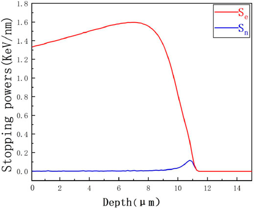
FIGURE 1. Electronic (red line) and nuclear (blue line) stopping powers as function of penetrate depth from the surface of the 15 MeV C5+ ion irradiated BaF2 crystal.
Because the waveguide fabricated by C5+ ion irradiation has high irradiation energy and deep buried layer, the refractive index distribution cannot be measured by dark mode spectroscopy directly. To obtain the refractive index profile of the waveguide at 4 µm wavelength, we measured the maximum refractive variation Δn by using the formula [22],
where n = 1.4568 is the refractive index of BaF2 crystal at 4 µm wavelength;
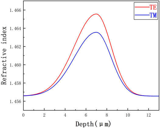
FIGURE 2. Refractive index profile on TE (red line) and TM (blue line) modes at 4 μm wavelength of the 15 MeV C5+ ion irradiated BaF2 crystal.
Figures 3A–C depict the measured near-field modal profile of the ridge waveguide at 4 µm wavelength along TE and TM polarizations, respectively. As we can see, the near-field modal profiles exhibit single-mode guidance on TE mode and multi-mode guidance on TM mode. It shows that the guiding characteristic at 4 µm wavelength on TE mode is superior compared to TM mode, which conforms to the measured Δn (TE) > Δn (TM). According to the reconstructed refractive index profile of the waveguide at 4 μm, we simulated the near-field modal profile of the waveguide using Rsoft software through finite difference beam propagation method (FD-BPM) on TE and TM modes, respectively, as shown in Figures 3B–D, which is in good agreement with the experimental results [23].
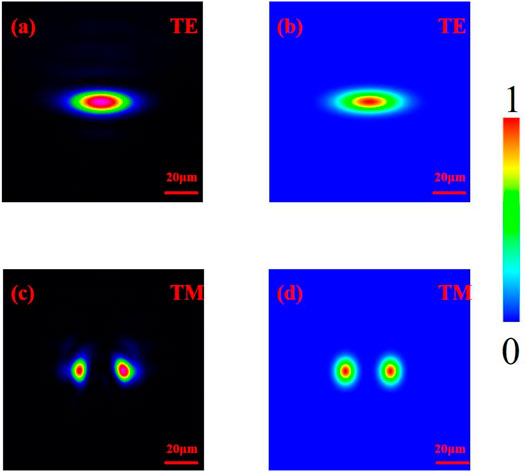
FIGURE 3. Measured near-field modal profiles (A) (C) and simulated modal profiles by using FD-BMP code (B) (D) of the ridge waveguide at 4 μm wavelength.
Figure 4 depicts the measured propagation losses of the ridge waveguide at 4 µm wavelength on TE and TM modes before and after each annealing treatment. As we can see, for TE mode, the propagation loss is 5.1 dB/cm before annealing. After 5 steps of annealing, the propagation loss decreases to 4.0 dB/cm (step 1, 210°C), 2.6 dB/cm (step 2, 240°C), 1.1 dB/cm (step 3, 270°C), 0.5 dB/cm (step 4, 300°C), and 0.5 dB/cm (step 5, 330°C). For TM mode, the propagation loss is 6.0 dB/cm before annealing. After 5 steps of annealing, the propagation loss decreases to 4.7 dB/cm (step 1, 210°C), 3.2 dB/cm (step 2, 240°C), 2.1 dB/cm (step 3, 270°C), 0.9 dB/cm (step 4, 300°C), and 0.9 dB/cm (step 5, 330°C). We can conclude that a series of annealing treatment (step 1–4, 210–330°C) can eliminate the color center and point defect of the waveguide region which can decrease the propagation loss of the waveguide. After step 5 annealing, the propagation loss of the waveguide remains unchanged and it shows the temperature range of 330–360°C is the thermal stability region of the waveguide. We can find that under the same annealing condition, the propagation loss of the waveguide at TE mode is lower than that at TM mode.
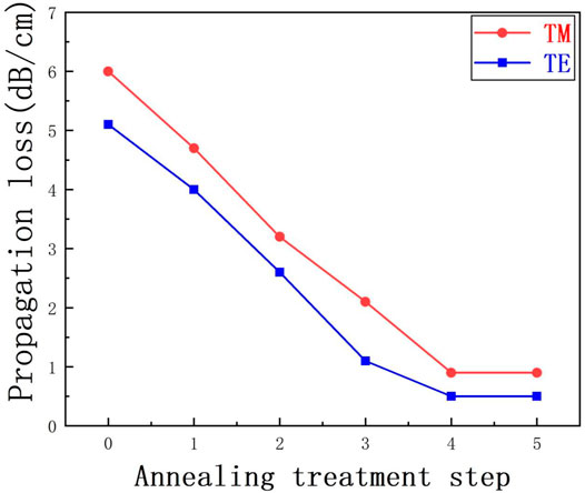
FIGURE 4. Propagation losses of BaF2 ridge waveguide at 4 μm wavelength on TE (blue line) and TM (red line) modes before and after each annealing step (1–5).
Figure 5 depicts the Raman spectrum of the waveguide and substrate of BaF2 crystal. As we can see, the Raman spectrum of the waveguide coincides with that of the substrate very well. It indicates that ion irradiation does not significantly damage the lattice of the crystal.
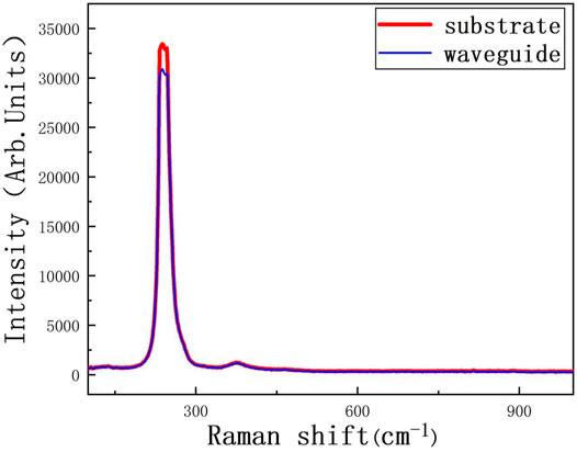
FIGURE 5. Raman spectra of 15 MeV C5+ ion irradiated BaF2 crystal in the waveguide region (blue line) and substrate region (red line).
We used technique of 15 MeV C5+ ions irradiation with femtosecond laser ablation to construct a ridge waveguide in BaF2 crystal and investigated the guiding properties at 4 µm wavelength. We simulated the energy deposition process of ion irradiation and reconstructed the refractive index profile of the waveguide. By using end-face coupling arrangement, we measured the near-field modal profile showing single-mode at TE and multi-mode at TM. After a series of annealing treatment, the propagation loss of the waveguide is reduced as low as 0.5 dB/cm on TE mode and 0.9 dB/cm on TM mode. The Raman spectrum shows that ion irradiation process does not damage the lattice of the crystal. Our work suggests an effective method to fabricate low-loss ridge waveguide structure in BaF2 crystal, which shows a prospective application in MIR integrated optical chips. In the further work, we consider to construct waveguides with more complex geometries.
The original contributions presented in the study are included in the article; further inquiries can be directed to the corresponding author.
YC proposed the original idea, wrote the paper, and supervised the project. XZ performed the experiments and measurements. HS supported the formal analysis. All authors contributed to the article.
The work was supported by the National Natural Science Foundation of China (NSFC) (No. 11805113), Natural Science Foundation of Guangdong Province (No. 2018A030313280), Project funded by China Postdoctoral Science Foundation (No. 2017M622192), Postdoctoral Innovation Special Foundation of Shandong Province (No. 201703008), Future Program for Young Scholars of Shandong University, and Fundamental Research Funds of Shandong University.
The authors declare that the research was conducted in the absence of any commercial or financial relationships that could be construed as a potential conflict of interest.
All claims expressed in this article are solely those of the authors and do not necessarily represent those of their affiliated organizations, or those of the publisher, the editors, and the reviewers. Any product that may be evaluated in this article, or claim that may be made by its manufacturer, is not guaranteed or endorsed by the publisher.
1. Wang N, Gu H. Diffusion Activation Energy of F Color Centers in Electrolytically Colored Barium Fluoride Crystals. J Synth Crystals (2014) 43(4):801–5.
2. Kelly-Gorham MRK, DeVetter BM, Brauer CS, Cannon BD, Burton SD, Bliss M, et al. Complex Refractive index Measurements for BaF2 and CaF2 via Single-Angle Infrared Reflectance Spectroscopy. Opt Mater (2017) 72:743–8. doi:10.1016/j.optmat.2017.06.052
3. Song X-Q, Du K, Li J, Lan X-K, Lu W-Z, Wang X-HX, et al. Low-Fired Fluoride Microwave Dielectric Ceramics with Low Dielectric Loss. Ceramics Int (2019) 45(1):279–86. doi:10.1016/j.ceramint.2018.09.164
4. Li XC, Wang CC, Zhao JM, Liu LH. Temperature-Dependent Optical Constants of Highly Transparent Solids Determined by the Combined Double Optical Pathlength Transmission-Ellipsometry Method. Appl Opt (2018) 57(5):1260–6. doi:10.1364/AO.57.001260
5. Wolf R, Jia Y, Bonaus S, Werner CS, Herr SJ, Breunig I, et al. Quasi-Phase-Matched Nonlinear Optical Frequency Conversion in On-Chip Whispering Galleries. Optica (2018) 5(7):872–5. doi:10.1364/OPTICA.5.000872
6. Jia Y, Wang S, Wang S, Chen F. Femtosecond Laser Direct Writing of Flexibly Configured Waveguide Geometries in Optical Crystals: Fabrication and Application. Opto-Electronic Adv (2020) 3(10):190042. doi:10.29026/oea.2020.190042
7. Chen F. Micro- and Submicrometric Waveguiding Structures in Optical Crystals Produced by Ion Beams for Photonic Applications. Laser Photon Rev (2012) 6(5):622–40. doi:10.1002/lpor.201100037
8. Chen F. Construction of Two-Dimensional Waveguides in Insulating Optical Materials by Means of Ion Beam Implantation for Photonic Applications: Fabrication Methods and Research Progress. Crit Rev Solid State Mater Sci (2008) 33(3-4):165–82. doi:10.1080/10408430802310868
9. Luan Q, Tan Y, Akhmadaliev S, Zhou S, Yu H, Zhang H, et al. Optical ridge Waveguides in Nd:CNGG Disorder Laser crystal Produced by Combination of Carbon Ion Irradiation and Precise diamond Blade Dicing. Opt Mater (2015) 39:247–50. doi:10.1016/j.optmat.2014.11.035
10. Jia Y, Wang L, Chen F. Ion-cut Lithium Niobate on Insulator Technology: Recent Advances and Perspectives. Appl Phys Rev (2021) 8(1):011307. doi:10.1063/5.0037771
11. Liu T, Yao Y-C, Liu F-R, Cheng L, Bao Y-F, Kong W-J, et al. Enhanced Raman Intensity in ZnS Planar and Channel Waveguide Structures via Carbon Ion Implantation. Opt Mater (2021) 112:110733. doi:10.1016/j.optmat.2020.110733
12. Tan Y, Luan Q, Liu F, Akhmadaliev S, Zhou S, Chen F. Swift Carbon Ion Irradiated Nd:YAG Ceramic Optical Waveguide Amplifier. Opt Express (2013) 21(12):13992–7. doi:10.1364/OE.21.013992
13. Tan Y, Chen F, Jaque D, Gao W-L, Zhang H-J, Solé JGJG, et al. Ion-Implanted Optical-Stripe Waveguides in Neodymium-Doped Calcium Barium Niobate Crystals. Opt Lett (2009) 34(9):1438–40. doi:10.1364/OL.34.001438
14. Tan Y, Jia Y, Chen F, Vázquez de Aldana JR, Jaque D. Simultaneous Dual-Wavelength Lasers at 1064 and 1342 Nm in Femtosecond-Laser-Written Nd:YVO_4 Channel Waveguides. J Opt Soc Am B (2011) 28(7):1607–10. doi:10.1364/JOSAB.28.001607
15. Yang Q, Liu H, Liu H, He S, Tian, Bin Xu Q, Wu P. Circular Cladding Waveguides in Pr:YAG Fabricated by Femtosecond Laser Inscription: Raman, Luminescence Properties and Guiding Performance. Opto-Electronic Adv (2021) 4(2):20000501–15. doi:10.29026/oea.2021.200005
16. Li R, Sun L, Cai Y, Ren Y, Liu H, Mackenzie MD, et al. Near-Infrared Lasing and Tunable Upconversion from Femtosecond Laser Inscribed Nd,Gd:CaF2 Waveguides. China Opt Lett (2021) 19(8):081301. doi:10.3788/COL202119.081301
17. Macdonald JR, Thomson RR, Beecher SJ, Psaila ND, Bookey HT, Kar AK. Ultrafast Laser Inscription of Near-Infrared Waveguides in Polycrystalline ZnSe. Opt Lett (2010) 35(23):4036–8. doi:10.1364/OL.35.004036
18. Chen C, Luan Q, He R, Cheng C, Akhmadaliev S, Zhou S, et al. Ridge Waveguides in Nd:ABC3O7 Disordered Crystals Produced by swift C5+ Ion Irradiation and Precise diamond Dicing: Broad Band Guidance and Spectroscopic Properties. Opt Laser Technol (2015) 68:84–8. doi:10.1016/j.optlastec.2014.11.017
19. Jia Y, Rüter CE, Akhmadaliev S, Zhou S, Chen F, Kip D. Ridge Waveguide Lasers in Nd:YAG Crystals Produced by Combining swift Heavy Ion Irradiation and Precise diamond Blade Dicing. Opt Mater Express (2013) 3(4):433–8. doi:10.1364/OME.3.000433
20. Jia Y, Dong N, Chen F, Vázquez de Aldana JR, Akhmadaliev S, Zhou S. Ridge Waveguide Lasers in Nd:GGG Crystals Produced by swift Carbon Ion Irradiation and Femtosecond Laser Ablation. Opt Express (2012) 20(9):9763–8. doi:10.1364/OE.20.009763
21. Ziegler JF. Computer Code. SRIM. Available at: http://www.srim.org.
22. Siebenmorgen J, Petermann K, Huber G, Rademaker K, Nolte S, Tünnermann A. Femtosecond Laser Written Stress-Induced Nd:Y3Al5O12 (Nd:YAG) Channel Waveguide Laser. Appl Phys B (2009) 97:251–5. doi:10.1007/s00340-009-3697-3
23.Rsoft Design Group. Computer Software BeamPROP Version 8.0. Available at: http://www.rsoftdesign.com.
Keywords: BaF2 crystal, mid-infrared, ridge waveguide, femtosecond laser ablation, ion irradiation
Citation: Cheng Y, Zhang X and Song H (2021) BaF2 Ridge Waveguide Operating at Mid-Infrared Wavelength. Front. Phys. 9:766905. doi: 10.3389/fphy.2021.766905
Received: 30 August 2021; Accepted: 13 September 2021;
Published: 14 October 2021.
Edited by:
Hongliang Liu, Nankai University, ChinaReviewed by:
Bingxi Xiang, Shenzhen Technology University, ChinaCopyright © 2021 Cheng, Zhang and Song. This is an open-access article distributed under the terms of the Creative Commons Attribution License (CC BY). The use, distribution or reproduction in other forums is permitted, provided the original author(s) and the copyright owner(s) are credited and that the original publication in this journal is cited, in accordance with accepted academic practice. No use, distribution or reproduction is permitted which does not comply with these terms.
*Correspondence: Yazhou Cheng, Y2hlbmd5YXpob3VAc2R1LmVkdS5jbg==
Disclaimer: All claims expressed in this article are solely those of the authors and do not necessarily represent those of their affiliated organizations, or those of the publisher, the editors and the reviewers. Any product that may be evaluated in this article or claim that may be made by its manufacturer is not guaranteed or endorsed by the publisher.
Research integrity at Frontiers
Learn more about the work of our research integrity team to safeguard the quality of each article we publish.