- 1School of Information Engineering, East China Jiaotong University, Nanchang, China
- 2State Key Laboratory of Millimeter Waves, Southeast University, Nanjing, China
- 3School of Electronics and Information Engineering, Jinggangshan University, Ji’an, China
In this paper, a novel dual-wideband balanced bandpass filter (BPF) based on branch-line structure is proposed. For analysis, the equivalent circuits of differential-mode (DM) and common-mode (CM) of the filter are built based on the even- and odd-mode method. With a proper synthesis design of DM bisection, dual passbands with a multi-order filtering response can be obtained. Additionally, three open-circuited stubs are centrally loaded on the CM bisection and six controllable transmission zeros are therefore generated. Thus, two stopbands are formed and then a favorable CM suppression within DM passbands is obtained. For demonstration, a third-order dual-wideband balanced BPF is designed with two passbands operating at 2.54 and 4.62 GHz. Good agreement between the simulated results and measured results is obtained, which verifies the validity of the proposed design method.
Introduction
Benefiting from the better anti-interference and robustness to unwanted and inevitable interference, such as electromagnetic noise, crosstalk, and the other different noise sources, e.g., coupled noise from adjacent circuitry and environmental noise, balanced microwave filters have been attracted much attention and widely used in modern high performance microwave transceivers in past few years [1].
Much efforts have been paid to the desired performances for these circuits of high selectivity and low insertion loss (IL) of differential-mode (DM) filtering function while high common-mode (CM) noise suppression [2]. However, these works are mainly focus on the single DM passband design with desired CM rejection level. The evolving of various modern communication systems providing multi-functional services, multi-band differential filters installed in versatile multimode RF architectures became new requisites [3].
In relation to the satisfied differential BPFs with multi-band characteristics, various technologies and topologies have been proposed, such as planar microstrip resonant structures [4–6], substrate integrated waveguide (SIW) technologies [7], slotline topologies [8], and 3-dimensional dielectric resonators [9]. In the meantime, considering for the circuit miniaturization, microstrip multimode resonant structures, such as the stepped impedance resonators [4], stub loaded resonators [5], and coupled-lines structures [6], are adopted to construct multiband differential BPFs. In addition, some more compact multimode resonators as well as the composite right/left transmission line structure are used for further reducing the circuit size [10]. However, the bandwidths of DM response in above works are narrow case with the relative bandwidths less than 10%, which can not meet the needs of broadband communicate scenarios. To our best knowledge, only one balanced filter with dual-wideband has been publicly reported [11]. However, the filter is constituted by slot-line structure, which needs the dual-layer microstrip process and increases the complexity in fabrication.
A newly dual-wideband balanced bandpass filter based on branch-line structure is proposed in this paper. Through the systematic design and optimization, two desirable wideband DM frequency responses with a good CM suppression within the DM passbands is achieved. The results of electromagnetic (EM) simulation verify the effectiveness of the design method.
Design Method of Dual-Band Bandpass Filter
Figure 1A portrays the basic topology of the cascaded nth-order dual-band BPF with J inverter, as demonstrated in [12]. Bn (i = 1, 2, 3…) indicates the shunt resonator. The adopted dual-band resonator is shown in Figure 1B, which constructed by shunting two open-circuited branch-lines and one shorted-circuited branch-line [13]. Y and θ indicate the corresponding characteristic admittance and electrical length. The below-line two open- and shorted-circuited branch-lines have same electric length θL. Two center frequencies of dual passbands are indicated as f1 and f2. Imposing the presented dual-band resonator into Figure 1A and replaces Bi, the circuit model of dual-band filter with series dual-band resonators is therefore obtained in Figure 2. All marked electric lengths are determined at f1. Note that the first and last admittance inverter can be removed by making J0 = 1/Z0, where Z0 is the terminal characteristic impedance.
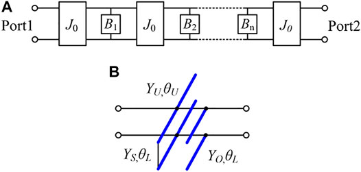
FIGURE 1. (A) Topology of the classical nth-order dual-band filter with dual-band J inverter (B) The adopted dual-band resonator.
For resonator 1 (R1) in Figure 2, five variables, YU1, θU1, YS1, YO 1, and θL1 are used to meet the requirements of the resonant frequencies and slope parameters at the two passbands. According to the classic filter synthesis method [14], it can be written as the following simultaneous equations:
where α is the ratio of f2 to f1, b1, b2 are the susceptance slope parameters at the resonance frequencies, gi (i = 0,1,2…) is the low-pass prototype value, and Δ1, Δ2 are the relative bandwidths of two passbands, respectively. In addition, the inverter is required to be the same at f1 and f2, so 1/sin2θL1 = 1/sin2αθL1 is obtained. The same synthesis method is also applied to design the other resonators in Figure 2.
By solving the Eqs 1–5, a very useful solution is found, i.e., when b2 = αb1, there is
At this time, all uncertain variables can be ascertained based on the desired specifications. Moreover, two parallel open- and short-circuited branch-lines can be equivalent to a short-circuited branch-line in the case of YS1 = YO 1, as the diagram shown in Figure 3A.
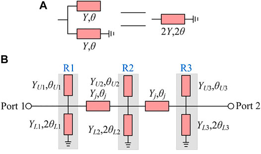
FIGURE 3. (A) Parallel equivalent diagram of open-circuited and short-circuited branch-lines (B) TLM of a third-order dual-band filter.
Based on the above analysis, a third-order transmission line model (TLM) of dual-band filter is obtained from transformed the Figure 2 and depicted in Figure 3B. Among them, the upper open-circuited branch-line and the below short-circuited branch-line constitute a new dual-band resonator. From the view of structure, it can be regarded as a stepped-impedance resonator. Thus, the overall circuit of Figure 3B is composed by three shunting resonators and two intermediate cascaded transmission lines (TLs). The intermediate cascaded TL is used to behave as the admittance inverter J0 in Figure 2 and equal to quarter-wavelength at fm, where fm is the average frequency of two passbands, i.e., (f1+f2)/2. The characteristic admittance Yj is equal to 0.02 S both for realization of J0 and a good impedance matching to signal ports.
Besides, αΔ2/Δ1 = 1 is obtained from the condition of b2 = αb1 and 5) and then, it is known that Δ2 is positively correlated with Δ1. Thus, two relative bandwidths of two passbands to be chosen in the later design need to meet this relationship. To further investigation, the variations of Δ1 versus the ZU1 (1/YU1) and ZL1 (1/YL1) at three different frequency ratios α are portrayed in Figure 4, based on Eqs 1–6. It is observed intuitively that Δ1 is increasing monotonically as either ZU1 or ZL1 is enlarged. However, the required ZU1 has a smaller value when frequency ratios α is larger in the case of realizing the same Δ1, as shown in Figure 4A, while ZL1 remains basically unchanged, as depicted in Figure 4B. Moreover, note that ZL1 will becomes a ultra small value when Δ1 is chosen to be a minor value, resulting in a very wide microstrip line and such that enlarge the circuit size. These imply that the proposed structure is more suitable and convenience in designing of larger frequency ratio and a wide bandwidth of dual-band balanced filter.
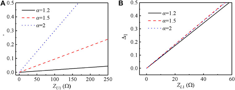
FIGURE 4. Calculated parameters of Figure 3B at different frequency ratios (A) The relationship between Δ1 and characteristic impedance ZU1(B) The relationship between Δ1 and characteristic impedance ZL1.
Implementation of Dual-Wideband Balanced Bandpass Filter
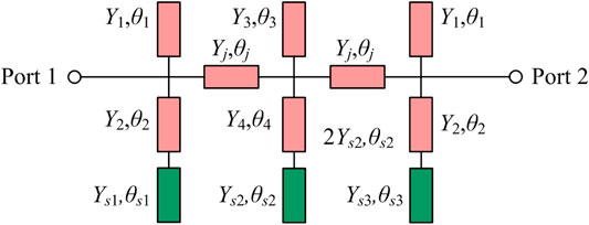
Based on the analysis in Design Method of Dual-Band Bandpass Filter Section, a third-order dual-wideband balanced BPF is proposed and its TLM is shown in Figure 5A. The desired two passbands are working at 2.52 and 4.65 GHz, respectively.
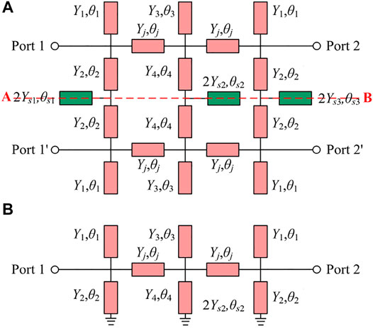
FIGURE 5. (A) TLM of the proposed third-order dual-wideband balanced BPF (B) Its DM equivalent circuit.
Differential-Mode Bisection
Since the filter is symmetrical about the red dashed line AB, even- and odd-mode analysis method can be used. With the excited by pair of DM (with respective to odd-mode) signals, the symmetry plane A-B behaves as an ideal electric wall, and then its DM equivalent circuit can be obtained, as depicted in Figure 5B. Observing the equivalent circuit of DM bisection, it is found that it has the same configuration with the TLM of Figure 3B. Therefore, the above presented method can be used to design the DM bisection.
Two DM passbands of the desired dual-wideband balanced BPF carrying Chebyshev filtering response with 0.01 dB ripple property are centered at 2.52 and 4.65 GHz with the corresponding relative bandwidth of 47.6 and 25.8%, respectively. Based on the analysis and design formulas in the previous section, the electric parameters are determined as: Y1 = 0.0048 S, Y2 = 0.019 S, Y3 = 0.0096 S, Y4 = 0.038 S, Yj = 0.02 S, θ1 = θ2 = θ3 = θ4 = 63.26° (@f1), and θ1 = 90° (@fm).
Simulated by ADS software, the obtained results of the DM bisection is portrayed as the red lines in Figure 6. It is seen that the center frequency and relative bandwidth of two passbands are 2.57 GHz (@ 47.5%) and 4.6 GHz (@ 27.0%), respectively, which agree with the design specifications.
Common-Mode Bisection
Similarly, when the even-mode signal is excited, the center line AB is virtually open-circuited and the symmetric plane acts as the magnetic wall, thus the CM equivalent circuit is obtained as shown in Figure 7. Three green TL stubs (Ys1&θs1, Ys2&θs2, Ys3&θs3) loaded at center portion are used to improve the CM suppression within the DM passbands. Because the CM and DM bisections are separated from the same TLM, so the branch lines in Figure 7 are quickly determined and maintain the same size as DM bisection except for the 3 TL stubs.
The simulated frequency response of CM bisection with removed the stubs as depicted the blue dashed line in Figure 6. It can be observed that the CM suppression within the DM passbands are not good and needs to be enhanced. The following is to discuss the effect of attached stubs. When only loading two stubs on the below branch lines of the first and the third resonator, the influence of the CM response is discussed and the corresponding results are shown in Figure 8. As illustrated in Figure 8A, two extra transmission zeros (TZs), fa1 and fb1, are produced when two stubs are identical and, they are respective located at two DM passband, compared with the case of without stubs. Moreover, the location of TZs can be adjusted by varying the characteristic admittance. Furthermore, two more TZs, fa2 and fb2, are created when the characteristic admittance of these two stubs are unequal, which widen the stopbands of CM response. Besides, the bandwidth of dual stopband can be tuned by changing the characteristic admittance.
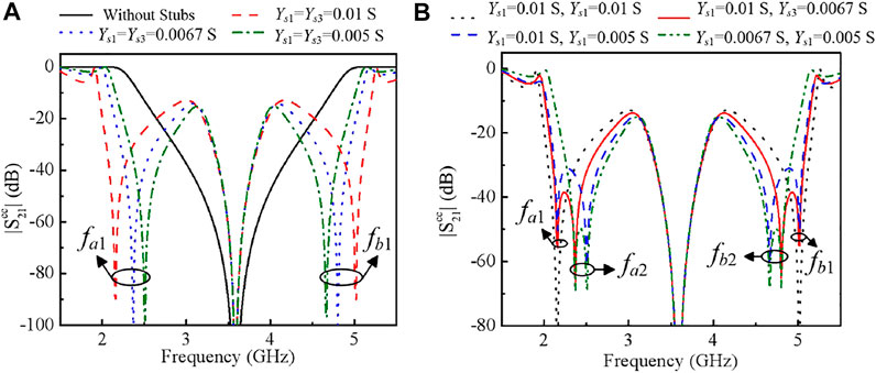
FIGURE 8. Simulated results of CM bisection with loading two stubs on the first and third resonator (A) Two identical stubs (B) Two different stubs.
Similarly, two additional TZs, fa3 and fb3, can be generated when the third stub is loading on the below branch line of the middle resonator, as portrayed in Figure 9A. Thus, six TZs in total can be provided for enhancing the CM suppression with the help of installing extra stubs on the proposed resonator. To investigate the generate mechanism of TZs, a circuit model is built as depicted in Figure 9B. Based on the basic TL theory, when Zin = 0, TZ is created. Thus, the frequency of six TZs can be expressed as.
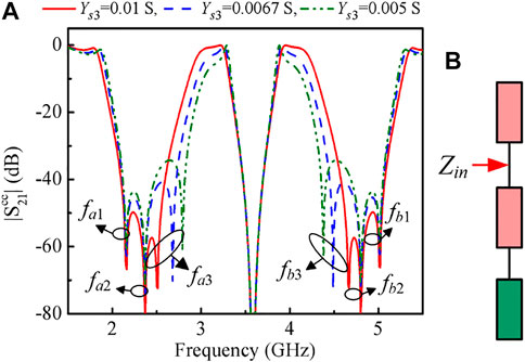
FIGURE 9. (A) The CM responses with varied Ys3 of the CM circuit when Ys1 = 0.01 S and Ys2 = 0.0067 S (B) The TLM of TZ generation.
It can be seen from Eqs 7–9 that when the DM bisection has been designed, the position of the TZs fa1, fb1 is only decided by Ys1 and, the position of fa2, fb2 is related to Ys2, and fa3, fb3 are determined by Ys3. Therefore, the position of the TZs can be independently controlled by adjusting the characteristic impedance of the loading stubs. As a result, the dual-stopband for CM suppression can be easily designed to satisfy the required specifications.
After well designed, the characteristic admittance of centrally loaded stubs are: Ys1 = 0.013 S, Ys2 = 0.0067 S, Ys3 = 0.005 S. Six TZs from the simulation of TLM located at 2.000, 2.370, 2.790, 4.380, 4.800, and 5.170 GHz, respectively, which agree well with the corresponding calculated results of 1.996, 2.367, 2.793, 4.378, 4.804, 5.175 GHz.
Conduction on Microstrip Configuration
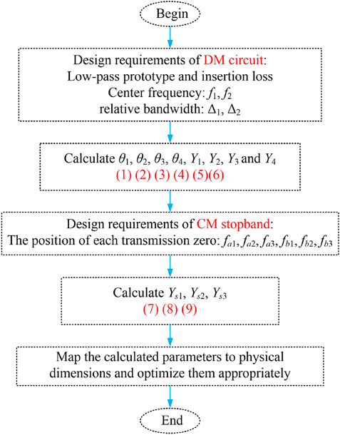
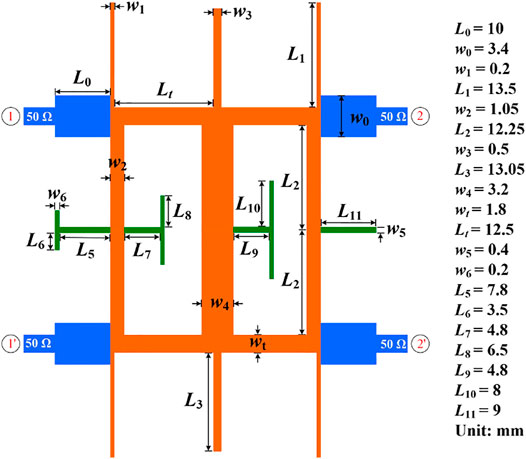
To clarify the overall design procedure, the crucial step of designing the proposed dual-wideband balanced bandpass filter is organized and given in Figure 10. Based on the discussion and determined electric parameters above, the microstrip model of the proposed dual-wideband balanced BPF is built and the layout is shown in Figure 11. The adopted substrate is Rogers 4003C with relative dielectric constant of 3.38, thickness of 0.813 mm, and loss tangent of 0.0027. The final dimensions are well optimized by em software and indicated in Figure 11. Note that the stepped-impedance feeding structure is employed to reduce the return loss of DM passband.
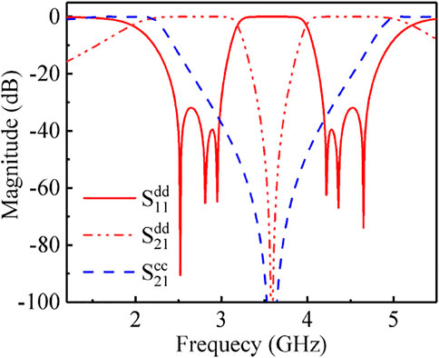
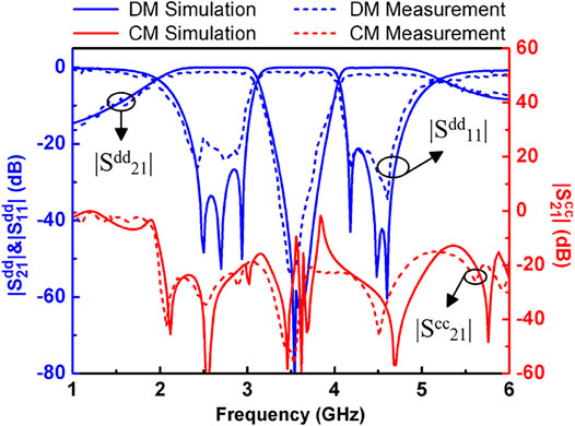
The EM simulated results is shown in Figure 12. As drawn by red solid lines, the center frequencies of two DM passbands are 2.54 and 4.6 GHz with the relative bandwidths of 45.2 and 26.6%, respectively. The return loss in the two passbands is better than 21 dB. The simulated CM response is indicated by blue solid line. It is observed that the CM stopbands can cover the corresponding DM passband completely, leading to the maximum and minimum CM suppression within the DM passband are 68 and 15.1 dB for the first passband and 56 and 15.4 dB for the second passband, respectively. Some deviations, both including the dimensions and results, are attributed to the parasitic effect of microstrip structure.
Measurement of the Fabricated Filter
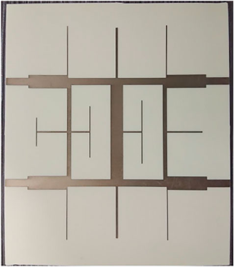
For verification, the designed dual-wideband balanced BPF is fabricated on the copper board with microstrip line process. The photograph is presented in Figure 13 and it occupies 45.9 × 55.1 mm2 with the feeding lines excluded.
The fabricated filter is measured by four-port network analyze of CETC 3671E. The measurements are portrayed as dashed-lines in Figure 12. As illustrated, the first DM passbands is measured at 2.54 GHz with covering 2.03–3.05 GHz and the second one is measured at 4.61 GHz with encompassing 4.1–5.12 GHz. The maximum IL within two passbands is 1.4 and 1.95 dB. Besides, the measured CM suppression within two DM passbands are better than 20 dB except at the edge of the passband and CM suppression has the minimum level of 15.3 dB.
In addition, Table 1 summarizes the comparison of the proposed filter with other dual-band balanced/differential filters that have been publicly reported. It reveals that the proposed filter is superior to other filters in terms of bandwidth of DM passband. However, the circuit size of the designed filter needs to be reduced compared with the ones of these reported works, and the insertion losses are relative large when compared with the ones demonstrated in [8, 9]. Besides, it is still observed from Figure 12 that the selectivity of the lower side-band of the first passband and the upper side-band of the second passband is not good. Some methods for TZ generation, such as adopting coupled-line structure and signal interference technique, can be further researched to improve the selectively. Meanwhile, the magnetic coupling or the microstrip-slotline conversion structure can be adopted to widen the scope of CM suppression in further studies.
Conclusion
A newly third-order dual-wideband balanced BPF is developed based on branch-line resonant structure in this work. The comprehensive design method of DM bisection with multi-order filtering response is presented. Besides, the attached stubs on the center plane of the CM bisection are well analyzed for dual-stopband property and such that enhancing the CM suppression. The proposed design method and filtering structure are validated well by the measured results.
Data Availability Statement
The original contributions presented in the study are included in the article/Supplementary Material, further inquiries can be directed to the corresponding authors.
Author Contributions
All authors listed have made a substantial, direct, and intellectual contribution to the work and approved it for publication.
Funding
This work was supported in part by the National Science Foundation of China (Nos 61761018, 61901170, 61861022), in part by the Science and Technology Plan Project of Jiangxi Province (Nos 20192BBE50063, 20202ACBL212002, 20204BCJ23007, 20192BAB217002), in part by the Project of Jiangxi Province Education Department (Nos GJJ190318, GJJ180313), in part by the Project of State Key Laboratory of Millimeter Wave (No. K202114), and in part by the Graduate Innovation Foundation of Jiangxi Province (No. YC 2020-S367).
Conflict of Interest
The authors declare that the research was conducted in the absence of any commercial or financial relationships that could be construed as a potential conflict of interest.
Publisher’s Note
All claims expressed in this article are solely those of the authors and do not necessarily represent those of their affiliated organizations, or those of the publisher, the editors and the reviewers. Any product that may be evaluated in this article, or claim that may be made by its manufacturer, is not guaranteed or endorsed by the publisher.
References
1. Feng W, Che W, Xue Q. The Proper Balance: Overview of Microstrip Wideband Balance Circuits with Wideband Common Mode Suppression. IEEE Microwave (2015) 16:55–68. doi:10.1109/mmm.2015.2408275
3. Gómez-García R, Loeches-Sánchez R, Psychogiou D, Peroulis D. Multi-stub-loaded Differential-Mode Planar Multiband Bandpass Filters. IEEE Trans Circuits Syst (2018) 65:271–5. doi:10.1109/tcsii.2017.2688336
4. Shi J, Xue Q. Dual-band and Wide-Stopband Single-Band Balanced Bandpass Filters with High Selectivity and Common-Mode Suppression. IEEE Trans Microwave Theor Techn (2010) 58:2204–12. doi:10.1109/tmtt.2010.2052959
5. Wu X, Wan F, Ge J. Stub-loaded Theory and its Application to Balanced Dual-Band Bandpass Filter Design. IEEE Microw Wireless Compon Lett (2016) 26:231–3. doi:10.1109/lmwc.2016.2537045
6. Yang L, Choi W-W, Tam K-W, Zhu L. Balanced Dual-Band Bandpass Filter with Multiple Transmission Zeros Using Doubly Short-Ended Resonator Coupled Line. IEEE Trans Microwave Theor Techn (2015) 63:2225–32. doi:10.1109/tmtt.2015.2431679
7. Shen Y, Wang H, Kang W, Wu W. Dual-band SIW Differential Bandpass Filter with Improved Common-Mode Suppression. IEEE Microw Wireless Compon Lett (2015) 25:100–2. doi:10.1109/lmwc.2014.2382683
8. Wei F, Qin P-Y, Guo YJ, Ding C, Shi XW. Compact Balanced Dual- and Tri-band BPFs Based on Coupled Complementary Split-Ring Resonators (C-CSRR). IEEE Microw Wireless Compon Lett (2016) 26:107–9. doi:10.1109/lmwc.2016.2517125
9. Chen J-X, Li J, Shi J. Miniaturized Dual-Band Differential Filter Using Dual-Mode Dielectric Resonator. IEEE Microw Wireless Compon Lett (2018) 28:657–9. doi:10.1109/lmwc.2018.2842681
10. Song Y, Liu HW, Zhao W, Wen P, Wang Z. Compact Balanced Dual-Band Bandpass Filter with High Common-Mode Suppression Using Planar Via-free CRLH Resonator. IEEE Microw Wireless Compon Lett (2018) 28:996–8. doi:10.1109/lmwc.2018.2873240
11. Guo X, Zhu L, Wu W. A Dual-Wideband Differential Filter on Strip-Loaded Slotline Resonators with Enhanced Coupling Scheme. IEEE Microw Wireless Compon Lett (2016) 26:882–4. doi:10.1109/lmwc.2016.2615023
12. Yim H -YA, Wong F-L, Cheng K -KM. “A New Synthesis Method for Dual-Band Microwave Filter Design with Controllable Bandwidth,” Proceeding of Asia-Pacific Microwave Conference. 11-14 Dec. 2007, Bangkok, Thailand, IEEE (2007).
Keywords: branch-line structure, balanced filter, common-mode suppression, dual-wideband, differential-mode
Citation: Ren B, Liu X, Guan X, Xu M and Zhang Z-C (2021) A Dual-Wideband Balanced Bandpass Filter Based on Branch-Line Structure With Controllable Common-Mode Suppression. Front. Phys. 9:764648. doi: 10.3389/fphy.2021.764648
Received: 25 August 2021; Accepted: 14 September 2021;
Published: 04 October 2021.
Edited by:
Gang Zhang, Nanjing Normal University, ChinaReviewed by:
Linping Feng, South China University of Technology, ChinaRui-Sen Chen, Foshan University, China
Copyright © 2021 Ren, Liu, Guan, Xu and Zhang. This is an open-access article distributed under the terms of the Creative Commons Attribution License (CC BY). The use, distribution or reproduction in other forums is permitted, provided the original author(s) and the copyright owner(s) are credited and that the original publication in this journal is cited, in accordance with accepted academic practice. No use, distribution or reproduction is permitted which does not comply with these terms.
*Correspondence: Xuehui Guan, eHVlaHVpZ3VhbkBnbWFpbC5jb20=; Zhi-Chong Zhang, ei56aGljaG9uZ0BqZ3N1LmVkdS5jbg==
 Baoping Ren
 Xinlei Liu1
 Zhi-Chong Zhang
