 Shunpeng Lu
 Yiping Zhang
 Ying Qiu2
 Dongxiang Luo
94% of researchers rate our articles as excellent or good
Learn more about the work of our research integrity team to safeguard the quality of each article we publish.
Find out more
ORIGINAL RESEARCH article
Front. Phys., 09 September 2021
Sec. Optics and Photonics
Volume 9 - 2021 | https://doi.org/10.3389/fphy.2021.752476
This article is part of the Research TopicPhysical Model and Applications of High-Efficiency Electro-Optical Conversion DevicesView all 24 articles
On the same micro-LED display panel, LED pixels are always operated with high and low biased voltages simultaneously to show different brightness and colors. Thus, it is vitally important to understand the effect of the heat transmission between LEDs under high and low biased voltages. In this work, we design two different LED groups: Group A is two LEDs bonded together for heat transmission and Group B is two LEDs separated from each other. Then, the two LEDs are operated at one fixed and one tuned biased voltage respectively in each group in a vacuum chamber and the efficiency of the two groups is studied both experimentally and numerically. Here, our experimental results demonstrate that Group A exhibits a maximum improvement of 15.36% in optical output power compared with Group B. The underlying reason is that the wall-plug efficiency of the LED with a voltage lower than photon voltage (V < ℏω/q) is surprisingly enhanced by elevated temperature owing to the heat transmission by the LED under a high biased voltage in Group A. Our further study shows that in such a low voltage region the improvement in the efficiency is attributed to the enhanced carrier concentrations with elevated temperature. On the other hand, the LED in Group A under a high biased voltage further raises the overall efficiency by alleviating the thermal droop due to reduced temperature. Device temperature measurement and numerical calculation of radiative recombination under different temperatures further support the superior performance of Group A LEDs. Our research results can act as the research prototype to design the high-efficient LED arrays for better energy recycling and thermal control.
Semiconductor optoelectronic materials and devices develop very fast recent decades [1–6]. InGaN/GaN based materials is one of the most promising materials for optoelectronic applications. As one of the most important devices, GaN-based light-emitting diodes (LEDs) are recognized as next-generation lighting sources and have become increasingly prevalent in the lighting, display, and optical communication industries owing to great advantages of high emission efficiency, long lifetime, robust reliability, multi-color properties, and low cost [7–10]. However, high self-heating and low heat dissipation are the critical issues needed to be addressed during the operation of LEDs. Therefore, extensive research and development efforts have been devoted to reducing the thermal heat generated in the InGaN/GaN-based LEDs to reduce the thermal droop, which rapidly drops the device efficiency under a high input electrical power especially in the high voltage regime
In this work, we propose a new approach on the device level to address thermal heat issues by connecting LEDs for thermal transmission and applying varied voltages to different LED devices. The proposed method is observed to achieve thermal harvesting in InGaN/GaN LEDs with improved optical output power, enhanced energy efficiency, and alleviated thermal droop. Device temperature measurement and numerical calculation of Energy recycling further support the superior edge of the proposed design. The findings in this work reveal the cooling potential of LEDs and can provide guidelines on thermal management in designing the high-efficient LED arrays, especially for the mini- and micro-LEDs applications, and support the possibility of removing the heat sink.
The blue InGaN/GaN MQW LED wafers used in this work were grown on (0001) c-plane pattern sapphire substrates using an AIXTRON close-coupled showerhead metal-organic chemical-vapor deposition (MOCVD) system. Initially, the epitaxial growth was grown on a 30-nm thick low-temperature GaN nucleation layer followed by a 4 µm unintentionally doped n-type GaN (u-GaN) layer. Then a 2 µm thick Si-doped n-GaN layer was grown with the Si doping concentration of 5 × 1018 cm−3. Subsequently, six pairs of InGaN/GaN MQWs were grown with a 3 nm thick quantum well (QW) and a 9 nm thick quantum barrier (QB). The indium composition of the InGaN layer was 18% and the emission peak wavelength of the grown samples was centered at ∼ 460 nm. After the MQWs, a 20 nm Al0.15Ga0.85N electron blocking layer (EBL) was grown, followed by a 150 nm thick Mg-doped p-GaN layer with the Mg doping concentration of 1 × 1018 cm−3. Finally, the in-situ 720°C thermal annealing treatment in N2 ambient was carried out to activate the Mg dopants. After epitaxial growth was completed, the LED wafers were fabricated into vertical structured LED chips with a dimension of 1 mm × 1 mm by standard fabrication and packing processes. To facilitate the experimental measurement of these LED devices within the varied temperature range, the InGaN/GaN LEDs used in this work are bare dies without encapsulation or packaging, which leads to slightly lower wall-plug efficiency values than commercial LED devices or ones with optimized light extraction architectures [35].
The optical output power of these LED devices used in this work was measured by Si-photodiode connected to the Thorlabs Dual Channel Optical Power and Energy Meter. And the surface temperature of these LED devices was measured by the TELOPS High-Speed IR Cameras, and meanwhile thermal couples were connected to these LED devices to double confirm the accuracy of the experimentally measured data. In order to reduce the devices’ thermal dissipation into the ambient, all the experimental measurements were carried out in a high vacuum ambient, which was achieved by allocating the LEDs into a chamber and then pumping down the chamber to a high vacuum with a vacuum pressure of 4.05 × 10⁻⁷ mBar. During all the measurements, all the data were collected after the LEDs had reached thermal equilibrium.
In order to precisely reveal the mechanism that how the temperature influences the LED performance, numerical calculations were conducted by the Advanced Physical Models of Semiconductor Devices (APSYS) simulator, which self-consistently solves the Schrödinger equation, continuity equation, and Poisson equation with proper boundary conditions. In the simulations, the Auger recombination coefficient was set to 1 × 1042 m6/s and 40% of the polarization charges were assumed such that 60% of the theoretical polarization charges were released because of the crystal strain relaxation by generating dislocations [42–44].
In the research community of InGaN/GaN-based LEDs, operating at elevated temperatures is considered always undesirable, as this causes thermal droop and therefore degrades the device efficiency. Due to this reason, various structures and external cooling designs have been deployed in III-nitride LEDs including modifying device architectures and providing external cooling designs to alleviate the thermal droop by reducing operating temperature. However, in contrast to the common knowledge and practice of operating GaN-based LEDs, the increased device temperature may not necessarily lead to the degradation of efficiency. According to the well-known ABC model [45], internal quantum efficiency (IQE) can be expressed as follows at a low current injection level:
where n is the carrier concentration, A is the Shockley-Read-Hall (SRH) nonradiative recombination rate, B is the radiative recombination rate, and C is the Auger nonradiative recombination rate. The SRH nonradiative recombination and Auger recombination has been reported to be increased with elevated temperature [46–48], however, the carrier concentration is significantly increased with the temperature, as shown in the equations below, which may improve the IQE in one certain voltage region [37, 49], especially in the low voltage region.
where ni is the intrinsic concentration, q is the elementary charge, V is the applied voltage, k is the Boltzmann constant, T is the temperature, Nc is the effective density of states at conduction band edge, Nv is the effective density of states at valence band edge, me* is the effective electron mass, mh* is the effective hole mass, me is the free electron mass, and Eg is the energy bandgap of the material. From the above Eqs 1–3, it can be understood that for a low voltage when the device temperature is increased, the carrier concentration is considerably increased, which leads to the improved radiative recombination and possibly causes the enhanced IQE even though the nonradiative recombination is simultaneously increased. In that case, the elevated temperature effect becomes beneficial.
More importantly, when it turns to the voltage region (qV < ℏω), the Peltier effect is changed from Peltier heat to Peltier cooling. The total heating power Qtotal (per unit area) generated in the LED device consisting of Peltier heat QPeltier (phonon emission or absorption), nonradiative recombination heat Qnonradiative, and Joule heat QJoule can be expressed as below:
where J is the injection current density, V is the applied voltage, and
where I is the injection current and Rs is the total series resistance of the LED device. As inferred from the above Eq. 5, the Peltier heat is changed to Peltier cooling when the applied voltage is lower than the photon voltage (ℏω/q). As InGaN/GaN LEDs are typically driven under high bias (qV > ℏω), the possible positive effect of the increased temperature is never taken into consideration in the LED designs, even less to utilize in the operation. Our hypothesis is that, when the operating voltage of InGaN/GaN LEDs falls into the bias region of V < ℏω/q, the elevated temperature should become beneficial and enhance the device efficiency due to the enhanced carrier concentrations. Normally, there are more than one LED device embedded in the common lighting lamps and they suffer from severe thermal droop due to the considerable thermal heat generated when the applied voltages are higher than ℏω/q. If the positive effect of the temperature can be utilized in the LED lamps or arrays, it will alleviate the thermal droop and boost energy efficiency.
Therefore, in this work, we propose a creative and simple approach to take advantage of the positive effect of temperature and achieve thermal harvesting by applying the varied voltages to different LED devices embedded in the LED arrays, which is in contrast to the common operation. In our design, these LED devices are biased at different voltages and the high voltage-biased LEDs are operated at the working voltage regime V > ℏω/q normally falling into the efficiency-droop, high-voltage region, in which the LEDs suffer from severe thermal droop and elevated temperature is undesirable. Thus, a large amount of thermal heat is generated in these LED devices while less heat is generated for the low voltage-biased ones whose voltages are within the high-efficiency, mid-voltage region (V < ℏω/q), in which Energy recycling occurs. All these LED devices are close to each other in physical distance, thus the thermal heat transition among these devices occurs if there is a temperature gradient among them. The superior edge of this proposed configuration lies in two aspects. Firstly, the thermal heat flow among these devices enables heating the low-biased LEDs so that the device temperature is elevated, and the device efficiency is improved owing to the enhanced Energy recycling and the increased carrier concentrations. Secondly, because much thermal heat is transferred out from the LEDs under high biased voltage, the alleviated thermal droop is obtained, which boosts the efficiency and improves the device lifetime. Thus, the total energy efficiency of the whole LED system is increased. Even more importantly, the thermal heat generated is recycled and utilized and the total device temperature is tuned, which allows more energy-saving and efficient operation.
In order to demonstrate the proposed configuration and investigate its performance and advantages, we simplify the proposed configuration into a two-combined-LEDs design (named Group A Combined-LEDs setup), in which two behavior-similar LEDs are attached to each other in the way of back-to-back for highly efficient thermal transmission as illustrated in Figure 1A. In this simplified design, two LEDs are directly attached to each other in order to minimize the heat loss during the transition and maximize the amount of thermal heat that the LED under low voltage can receive. In this way, the beneficial effect of thermal heat can be maximized. This simplified configuration can be regarded as the research prototype and basic component for the LED arrays and the findings in the simplified model can be multiplied and applied to the whole LED arrays. A control group (called Group B Separated-LEDs setup) is also introduced as shown in Figure 1A by separating two LEDs far away from each other to eliminate the heat flow or any interference between them.
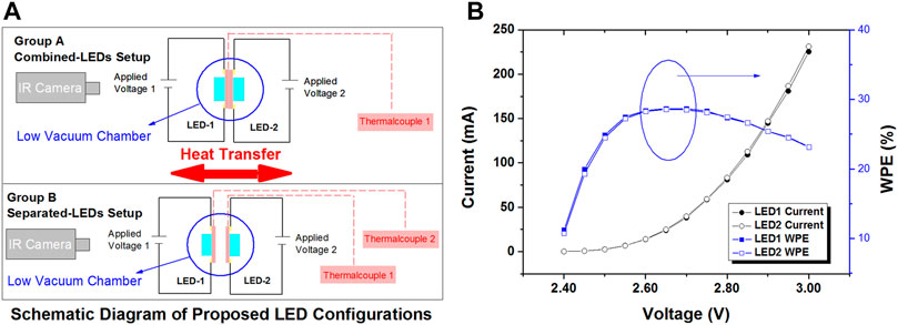
FIGURE 1. (A) Schematic diagram of the experimental measurements for proposed LEDs configuration (Group A) and the control group (Group B); (B) Experimental measured I-V curve and WPE versus applied voltages for two behavior-similar LEDs.
Figure 1B shows the experimental measured I-V curve and wall-plug efficiency (WPE) curve for two behavior-similar LEDs. It can be clearly seen from Figure 1B that both the electrical and optical behaviors of two LEDs used in the experiments are similar when the applied voltage is increased from 2.40 to 3.00 V. Due to the high similarity between these two LEDs, it is reasonable to believe that the influence of such minor variation in the performance of these two LEDs on the experimental results is limited. In order to investigate the overall performance of the proposed design and demonstrate its advantages, the experimental measurements are conducted in the way that the applied voltage for one of the LEDs (called LED-1) is changing (increased from 2.40 to 3.00 V), while the voltage of the other one (LED-2) is fixed at several values (2.40, 2.60, 2.80, and 3.00 V). The experimental measurements are carried out in a high vacuum chamber to reduce the heat dissipation into the ambient. Here, these two LEDs are regarded as one system, hence the coupled energy efficiency (CEE) of these two LEDs is calculated by:
Figures 2A–D show the experimental measured CEE of the system versus the applied voltage of LED-1, while LED-2 under a fixed voltage of 2.40, 2.60, 2.80, and 3.00 V for the Combined-LEDs and Separated-LEDs setups. When LED-2 is fixed at 2.4 V, as shown in Figure 2A, the proposed approach Group A Combined-LEDs has a higher CEE than the control group Group B separated LEDs at all voltages of LED-1. Such improvement is attributed to two aspects. On one hand, for LED-2 whose voltage is fixed at 2.40 V, Group A in the proposed configuration allows the thermal heat transition so that the thermal heat generated in the whole system can be easily absorbed by LED-2 before dissipating into the ambient and transfer the energy to the carriers through the Energy recycling. Thus, improve the efficiency of LED-2. On the other hand, for LED-1 whose voltage is increased from 2.40 to 3.00 V, when the voltage is lower than photon voltage (2.69 V in our case) the elevated temperature and enhanced Energy recycling because of a smaller heat dissipation area contribute to the improved efficiency. When the voltage is increased to a value higher than photon voltage, the effect of elevated temperature turns to negative for LED-1. However, in our designed LED group A, the LED-2 acts as the heat sink by absorbing part of the thermal heat generated by LED-1, which significantly reduces the device temperature of LED-1, thus leading to alleviated thermal droop and improved efficiency for LED-1. While it is worth noting that at the voltage of 2.40 V, Group A has a higher CEE than Group B. This is because the back-to-back bonded LEDs Group A has a smaller heat dissipation area than that of Group B. Based on our calculation, the heat dissipation area of group A is 3.76 mm2 and the heat dissipation area of group B is 5.76 mm2 for two LEDs. Hence, Group A holds more heat, which contributes to improved efficiency enhanced by Energy recycling and higher current density improved by the heat. The trend in Figure 2B is almost the same as that in Figure 2A, except for one small voltage region around 2.60 V, which will be analyzed in the following discussion. The proposed setup also outperforms the control group when the voltage of LED-1 is in the low voltage region even though the voltage of LED-2 is increased to 2.80 and 3.00 V, as shown in Figures 2C,D . However, when the voltage variation between LED-1 and LED-2 gets smaller even negative, the lower heat dissipation capability of the Combined-LEDs setup with back-to-back configuration causes more severe thermal droop than the Separated-LEDs setup, thus degrading the efficiency, as shown in the high voltage regions of Figures 2C,D. It is noteworthy that when the variation of these two LEDs becomes larger, the LED with lower voltage plays the role of heat sink even though the voltages of both two LEDs are higher than photon voltage, for example, VLED-1 = 2.80 V, VLED-2 = 3.00 V, and VLED-1 = 3.00 V, VLED-2 = 2.80 V. Further analysis of the experimental measured CEE curves versus the total electrical input of two LEDs for two setups presented in Figures 2E,F,G,H also show the same trend. The improvement in the CEE of the presently studied configuration becomes relatively more pronounced when the applied voltage of LED-2 increased to 3.00 V.
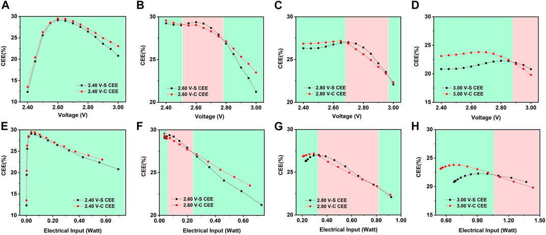
FIGURE 2. Experimental measured CEE for two LED groups versus applied voltage of LED-1, while LED-2 under a fixed voltage of (A) 2.40, (B) 2.60, (C) 2.80, and (D) 3.00 V; CEE versus total electrical power for two LED groups, while LED-2 under a fixed voltage of (E) 2.40, (F) 2.60, (G) 2.80, and (H) 3.00 V. Here, V-C is Group A combined LED setup and V-S is Group B Separated-LEDs setup.
Further analysis of the optical output power shown in Figure 3 gives a peak power improvement of 19.95 mWatt (15.65% in terms of percentage) for the proposed configuration Group A studied here compared to the control group. The results in Figure 3 suggest that under the same electrical input the proposed configuration with varied voltages has higher optical output power than the control group when the electrical input is smaller than 1.02 Watt. This improvement originates mainly from the beneficial effect of the increased temperature of the low-biased LED, as well as the alleviated thermal droop in the high-biased LED. Such improvement in the performance of the Combined-LEDs setup becomes relatively more pronounced under low electrical input. It is worth mentioning that the starting point of group A is smaller than that of group B, as indicated in Figure 3. The difference in the starting point of the electrical input between these two groups is due to the difference of the current for the whole system caused by the varied temperature. As LED-2 is under a voltage of 3.00 V for both groups and group A is two LEDs combined together for good heat transmission, LED-2 in group A has lower temperature and smaller current than that of group B, and LED-1 in group A has higher temperature and larger current than that of group B. We further calculate the current of LED-2 for two groups. The current of LED-2 for group A is 180 mA and that for group B is 230 mA. As the electrical input of LED-2 dominates the electrical input for two groups at the start point, the starting point of group A is smaller than that of group B.
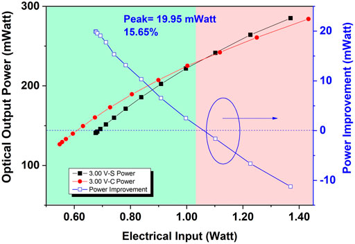
FIGURE 3. The total optical output power versus total electrical input for two setups and corresponding power improvement for group A compared to group B. Here, LED-2 is under a voltage of 3.00 V for both groups. V-C is Group A combined LED setup and V-S is Group B Separated-LEDs setup.
Figure 4A presents the device surface temperature of LEDs versus applied voltage of LED-1 for two setups with VLED-2 = 3.00 V, from which we can see that the device temperature of LED-2 in the proposed model is reduced compared to that in the control group at most of the voltages with a maximum reduction of 40 K at the voltage of 2.40 V. Such reduction becomes smaller with the increasing voltage and eventually changes to negative when the applied bias is higher than 2.85 V. In contrast to LED-2, the temperature of LED-1 in Group A is increased at all the voltages and the increase becomes smaller with the increasing applied biased voltage. It is worth noting that the temperature of Group A is a little higher than that of the control group (the average of the temperatures of LED-1 and LED-2) and the variation between them becomes more considerable with the increase of the applied bias. Such variation is caused by the difference in heat dissipation capability between two groups during the experimental measurement, which cannot be neglected when the input electrical power is high even though the measurement is carried out in the high vacuum chamber to reduce the thermal heat dissipation to the ambient.
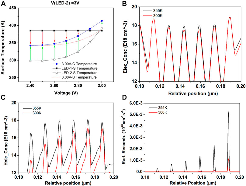
FIGURE 4. (A). The device temperature of LEDs versus applied voltage for Combined-LEDs and Separated-LEDs setups with the voltage of LED-2 fixed at 3.00 V. Numerical results of the (B) electron concentration, (C) hole concentration, and (D) radiative recombination rate in the InGaN/GaN LEDs with the device temperature of 300 and 355 K under the voltage of 2.6 V.
To further support the claim that the elevated temperature caused by the heat absorption contributes to a higher average kinetic energy of the carrier and higher carrier concentration in the quantum wells, numerical calculation of the electron and hole concentrations, and the radiative recombination rate in the LEDs is conducted. Figures 4B,C show the calculated electron and hole concentrations of the InGaN/GaN LEDs at temperatures of 300 K and 355 K under the voltage of 2.6 V, from which it can be seen that the electron and hole concentrations increase at a higher temperature, suggesting that the total energy absorbed by the carriers from the phonon field is increased when the carriers climb up the potential barriers. The carriers overcome the potential barrier under the force of the electrical field, while for those without sufficient energy, the remaining energy is drawn from the phonon field to overcome the potential barriers. From Figure 4D, we can also observe that the radiative recombination rate is enhanced as the electron and hole concentrations increased due to higher temperature. Therefore, the elevated temperature leads to an increased carrier concentration, thus the improved efficiency is obtained in the voltage region of V ≲ ℏω/q. The improved performance in the proposed configuration is mainly caused by the elevated temperature that leads to increased carrier concentration, and minor reduced energy bandgap under the small and moderate electrical input [50, 51]. However, when the applied voltage is increased to further higher, e.g., 3.00 V in our experiments where the LED suffers from serious thermal droop, the contribution of the elevated temperature effect turns negative. Thus the proposed setup shows inferior performance due to its smaller thermal dissipation area compared to the control group, as indicated in Figure 3.
In order to further support the advantages of applying varied biases in the proposed approach, the measurements are modified to bias two LEDs at the same voltage simultaneously. Figure 5 shows the measured CEE as a function of applied voltage and input electrical power, from which an enhanced CEE in the Combined-LEDs setup compared to the Separated-LEDs setup is observed when the applied voltage is smaller than 2.50 V and the corresponding electrical power of 12.77 mWatt is much lower than 19.95 mWatt shown in Figure 3. Furthermore, the maximum improvement in the CEE is also much lower than that observed in Figure 3, which further supports the superior edge of applying varied biases in the studied setup.
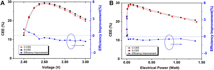
FIGURE 5. (A) Experimental CEE and corresponding efficiency improvement for modified Combined-LEDs and Separated-LEDs setups versus applied voltage and (B) electrical input power.
In order to further investigate the underlying mechanism of the enhanced performance in the proposed approach, the wall-plug efficiency and device temperature of LED-1 are also identified for the Combined-LEDs setup and Separated-LEDs setup, as shown in Figure 6. It can be clearly seen from Figure 6B that the device temperature of LED-1 in the case of VLED-2 = 3.00 V is always higher than that in the control group. Due to such increase, as shown in Figure 6A, the LED-1 is observed to have a pronounced enhancement in efficiency with a maximum improvement of 5.93% (27.91% in terms of percentage) in the proposed setup when the voltage is lower than 2.70 V. It can be clearly seen that the influence of temperature on efficiency varies in different operating regions separately by one inflection points: High-efficiency, Mid-voltage Region (2.15 V < V < 2.70 V); and Efficiency-droop, High-voltage Region (V ≥ 2.70 V). While the efficiency becomes worsen than that in the control group when the applied voltage of LED-1 is further increased to higher than 2.70 V (efficiency-droop, high-voltage region). The analysis of the device temperature and measured WPE for LED-1 in the Combined-LEDs setup and control group suggest that the increased temperature has a beneficial effect on device efficiency when the operating voltage falls in the high-efficiency, mid-voltage region due to the increased spontaneous radiative as well as the enhanced Energy recycling which allows the carriers to absorb the remaining energy from thermal heat as shown in Figure 4B . However, the effect of elevated temperature becomes negative when the applied voltage is increased to the efficiency-droop, high-voltage region, where the increased temperature leads to the more serious carrier overflow, reduced hole injection efficiency, and Auger recombination [52].
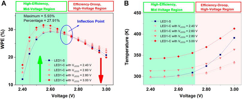
FIGURE 6. (A) The WPE and (B) device temperature of LED-1 as a function of applied voltage for the Separated-LEDs and Combined-LEDs setups under VLED-2 = 2.40, 2.60, 2.80, and 3.00 V.
As indicated in Figure 6A the voltage corresponding to the peak efficiency for LED-1 is around 2.60 V and is slightly shifted with the increasing temperature. However, the corresponding current density at which the efficiency reaches the maximum remains constant. According to Eq. 1, the peak efficiency of IQE is achieved when [45, 53]:
Hence, the carrier concentration corresponding to the maximum efficiency is obtained at
where J0 is the current density at n0, and e is the elementary electronic charge while v is the carrier drift velocity. Therefore, the peak-efficiency current density is almost constant with the increased temperature. Since the elevated temperature leads to the increased current, the peak-efficiency current density can be achieved under lower voltage. For both LED-1 and LED-2 without combined configuration, the peak-efficiency current is around 13.86 mA, corresponding to the voltage of 2.60 V. Thus, the elevated temperature in the proposed setup will drive the efficiency away from the peak efficiency when the voltages of the two LEDs are close to 2.60 V, as shown in the Figure 2B.
Even though the LEDs are always driven by constant current and have additional cooling architectures, the thermal issues remain a great challenge for GaN-based LEDs, and achieving thermal dissipation through external architecture needs more space thus increasing the design difficulty of the system. Furthermore, using a larger size LED device is a common approach to increase the total optical output power with the heating issues remaining. Thus, the method proposed in this work provides an alternative way to achieve the desired total output power simultaneously recycling the thermal heat and achieving thermal harvesting. More importantly, the proposed approach is more promising to address thermal issues in some specific situations, for example, Ribbon Filament LED, which has no additional space to add the external cooling architectures because all the LEDs are allocated along the filament.
To conclude, in this work, we propose and demonstrate a new design to address the challenge in thermal heat issues, as supported by experiments, by recycling the thermal heat. The elevated temperature is found to be beneficial due to enhanced carrier concentrations and Energy recycling when the applied voltage is lower than the photon voltage. We present experimental results emphasizing the superior edge of the proposed configuration, in which with the varied biases applied to two LEDs, the thermal heat is exchanged and absorbed by the carriers thus the improved efficiency of the whole system through Energy recycling and thermal harvesting is achieved. Furthermore, owing to heat transmission the high-biased LED succeeds in reducing the device temperature and alleviating the thermal droop. Such a superior edge of the studied approach may become pronounced when exploited to the ribbon LED lamp, in which the space for designing and allocating the chips is limited and the LEDs arrangement is critical in the point of thermal management. Due to the advantages of the proposed setup, this method can act as an extremely useful intermediate research prototype to design the high-efficient LED arrays and achieve better energy recycling and thermal control, especially for mini- and micro-LEDs. Lastly, these findings in this work further support the possibility to remove the heat sink.
The original contributions presented in the study are included in the article/Supplementary Material, further inquiries can be directed to the corresponding authors.
SL and YZ contribute to this work equally. All authors reviewed the paper.
This work is supported by the Guangdong Basic and Applied Basic Research Foundation (Grant No. 2020B1515020032, 2020B1515120022), the National Natural Science Foundation of China (Grant No. 62074060), the Guangdong Science and Technology Plan (Grant No. 2019B040403003) and the Pearl River S&T Nova Program of Guangzhou (Grant No. 201906010058).
The authors declare that the research was conducted in the absence of any commercial or financial relationships that could be construed as a potential conflict of interest.
All claims expressed in this article are solely those of the authors and do not necessarily represent those of their affiliated organizations, or those of the publisher, the editors, and the reviewers. Any product that may be evaluated in this article, or claim that may be made by its manufacturer, is not guaranteed or endorsed by the publisher.
1. Pimputkar S, Speck JS, DenBaars SP, Nakamura S. Prospects for LED Lighting. Nat Photon (2009) 3:180–2. doi:10.1038/nphoton.2009.32
2. Khan A, Balakrishnan K, Katona T. Ultraviolet Light-Emitting Diodes Based on Group Three Nitrides. Nat Photon (2008) 2:77–84. doi:10.1038/nphoton.2007.293
3. Tian S, Sui F, He K, Cheng G, Ge Y, Ning D, et al. Co-Axial Silicon/Perovskite Heterojunction Arrays for High-Performance Direct-Conversion Pixelated X-ray Detectors. Nano Energy (2020) 78:105335. doi:10.1016/j.nanoen.2020.105335
4. Chen M, Wang Z, Ge X, Wang Z, Fujisawa K, Xia J, et al. Controlled Fragmentation of Single-Atom-Thick Polycrystalline Graphene. Matter (2020) 2:666–79. doi:10.1016/j.matt.2019.11.004
5. Nakamura S, Mukai T, Senoh M. Candela‐Class High‐Brightness InGaN/AlGaN Double‐Heterostructure Blue‐Light‐Emitting Diodes. Appl Phys Lett (1994) 64:1687–9. doi:10.1063/1.111832
6. Zhang Y, Lu S, Qiu Y, Wu J, Zhang M, Luo D. Experimental and Modeling Investigations of Miniaturization in InGaN/GaN Light-Emitting Diodes and Performance Enhancement by Micro-Wall Architecture. Front Chem (2021) 8:8. doi:10.3389/fchem.2020.630050
7. Tanaka S, Zhao Y, Koslow I, Pan C-C, Chen H-T, Sonoda J, et al. Droop Improvement in High Current Range on PSS-LEDs. Electron Lett (2011) 47:335–6. doi:10.1049/el.2010.3306
8. Ponce FA, Bour DP. Nitride-Based Semiconductors for Blue and Green Light-Emitting Devices. Nature (1997) 386:351–9. doi:10.1038/386351a0
9. Kobayashi Y, Kumakura K, Akasaka T, Makimoto T. Layered Boron Nitride as a Release Layer for Mechanical Transfer of GaN-Based Devices. Nature (2012) 484:223–7. doi:10.1038/nature10970
10. Lu S, Zhang Y, Zhang Z-H, Tsai PC, Zhang X, Tan ST, et al. Strain-Reduced Micro-LEDs Grown Directly Using Partitioned Growth. Front Chem (2021) 9:9. doi:10.3389/fchem.2021.639023
11. Liu L, Yang J, Ling M, Zhong J, Teng D, Wang G. Aggravated Efficiency Droop in Vertical-Structured Gallium Nitride Light-Emitting Diodes Induced by High Temperature Aging. J Appl Phys (2013) 113:083105. doi:10.1063/1.4790594
12. Choi S, Kim HJ, Kim S-S, Liu J, Kim J, Ryou J-H, et al. Improvement of Peak Quantum Efficiency and Efficiency Droop in III-Nitride Visible Light-Emitting Diodes With an InAlN Electron-Blocking Layer. Appl Phys Lett (2010) 96:221105. doi:10.1063/1.3441373
13. David A, Gardner NF. Droop in III-Nitrides: Comparison of Bulk and Injection Contributions. Appl Phys Lett (2010) 97:193508. doi:10.1063/1.3515851
14. Ryu H-Y, Shin D-S, Shim J-I. Analysis of Efficiency Droop in Nitride Light-Emitting Diodes by the Reduced Effective Volume of InGaN Active Material. Appl Phys Lett (2012) 100:131109. doi:10.1063/1.3698113
15. Vaxenburg R, Lifshitz E, Efros AL. Suppression of Auger-Stimulated Efficiency Droop in Nitride-Based Light Emitting Diodes. Appl Phys Lett (2013) 102:031120. doi:10.1063/1.4789364
16. Jung E, Hwang G, Chung J, Kwon O, Han J, Moon Y-T, et al. Investigating the Origin of Efficiency Droop by Profiling the Temperature across the Multi-Quantum Well of an Operating Light-Emitting Diode. Appl Phys Lett (2015) 106:041114. doi:10.1063/1.4907177
17. Meneghini M, De Santi C, Tibaldi A, Vallone M, Bertazzi F, Meneghesso G, et al. Thermal Droop in III-Nitride Based Light-Emitting Diodes: Physical Origin and Perspectives. J Appl Phys (2020) 127:211102. doi:10.1063/5.0005874
18. Lu S, Liu W, Zhang Z-H, Tan ST, Ju Z, Ji Y, et al. Low Thermal-Mass LEDs: Size Effect and Limits. Opt Express (2014) 22:32200–7. doi:10.1364/oe.22.032200
19. Han N, Viet Cuong T, Han M, Deul Ryu B, Chandramohan S, Bae Park J, et al. Improved Heat Dissipation in Gallium Nitride Light-Emitting Diodes With Embedded Graphene Oxide Pattern. Nat Commun (2013) 4:1452. doi:10.1038/ncomms2448
20. Liou B-H, Chen C-M, Horng R-H, Chiang Y-C, Wuu D-S. Improvement of Thermal Management of High-Power GaN-Based Light-Emitting Diodes. Microelectronics Reliability (2012) 52:861–5. doi:10.1016/j.microrel.2011.04.002
21. Horng RH, Chiang CC, Hsiao HY, Zheng X, Wuu DS, Lin HI. Improved Thermal Management of GaN/Sapphire Light-Emitting Diodes Embedded in Reflective Heat Spreaders. Appl Phys Lett (2008) 93:111907. doi:10.1063/1.2983740
22. He W, Zhang G, Zhang X, Ji J, Li G, Zhao X. Recent Development and Application of Thermoelectric Generator and Cooler. Appl Energ (2015) 143:1–25. doi:10.1016/j.apenergy.2014.12.075
23. Lu S, Zhang Y, Zhang Z-H, Zhu B, Zheng H, Tan ST, et al. High-Performance Triangular Miniaturized-LEDs for High Current and Power Density Applications. ACS Photon (2021) 8:2304–10. doi:10.1021/acsphotonics.1c00430
24. Tang B, Miao J, Liu Y, Wan H, Li N, Zhou S, et al. Enhanced Light Extraction of Flip-Chip Mini-LEDs with Prism-Structured Sidewall. Nanomaterials (2019) 9:319. doi:10.3390/nano9030319
25. Son KR, Lee TH, Lee BR, Im HS, Kim TG. Nitride-Based Microlight-Emitting Diodes Using AlN Thin-Film Electrodes With Nanoscale Indium/Tin Conducting Filaments. Small (2018) 14:1801032. doi:10.1002/smll.201801032
26. Park S-I, Xiong Y, Kim R-H, Elvikis P, Meitl M, Kim D-H, et al. Printed Assemblies of Inorganic Light-Emitting Diodes for Deformable and Semitransparent Displays. Science (2009) 325:977–81. doi:10.1126/science.1175690
27. Zhang K, Liu Y, Kwok H-s., Liu Z. Investigation of Electrical Properties and Reliability of GaN-Based Micro-LEDs. Nanomaterials (2020) 10:689. doi:10.3390/nano10040689
28. Wu T, Sher C-W, Lin Y, Lee C-F, Liang S, Lu Y, et al. Mini-LED and Micro-LED: Promising Candidates for the Next Generation Display Technology. Appl Sci (2018) 8:1557. doi:10.3390/app8091557
29. Lin JY, Jiang HX. Development of MicroLED. Appl Phys Lett (2020) 116:100502. doi:10.1063/1.5145201
30. Kang C-M, Kong D-J, Shim J-P, Kim S, Choi S-B, Lee J-Y, et al. Fabrication of a Vertically-Stacked Passive-Matrix Micro-LED Array Structure for a Dual Color Display. Opt Express (2017) 25:2489–95. doi:10.1364/oe.25.002489
31. Huang Y, Hsiang E-L, Deng M-Y, Wu S-T. Mini-LED, Micro-LED and OLED Displays: Present Status and Future Perspectives. Light Sci Appl (2020) 9:105. doi:10.1038/s41377-020-0341-9
32. Dousmanis GC, Mueller CW, Nelson H, Petzinger KG. Evidence of Refrigerating Action by Means of Photon Emission in Semiconductor Diodes. Phys Rev (1964) 133:A316–A318. doi:10.1103/physrev.133.a316
33. Piprek J, Li Z-M. Electroluminescent Cooling Mechanism in InGaN/GaN Light-Emitting Diodes. Opt Quant Electron (2016) 48:472. doi:10.1007/s11082-016-0729-1
34. Hurni CA, David A, Cich MJ, Aldaz RI, Ellis B, Huang K, et al. Bulk GaN Flip-Chip Violet Light-Emitting Diodes With Optimized Efficiency for High-Power Operation. Appl Phys Lett (2015) 106:031101. doi:10.1063/1.4905873
35. Xue J, Zhao Y, Oh S-H, Herrington WF, Speck JS, DenBaars SP, et al. Thermally Enhanced Blue Light-Emitting Diode. Appl Phys Lett (2015) 107:121109. doi:10.1063/1.4931365
36. Sadi T, Radevici I, Oksanen J. Thermophotonic Cooling With Light-Emitting Diodes. Nat Photon (2020) 14:205–14. doi:10.1038/s41566-020-0600-6
37. Santhanam P, Gray DJ, Ram RJ. Thermoelectrically Pumped Light-Emitting Diodes Operating Above Unity Efficiency. Phys Rev Lett (2012) 108:097403. doi:10.1103/PhysRevLett.108.097403
38. Li N, Han K, Spratt W, Bedell S, Ott J, Hopstaken M, et al. Ultra-low-Power Sub-Photon-Voltage High-Efficiency Light-Emitting Diodes. Nat Photon (2019) 13:588–92. doi:10.1038/s41566-019-0463-x
39. Radevici I, Tiira J, Sadi T, Ranta S, Tukiainen A, Guina M, et al. Thermophotonic Cooling in GaAs Based Light Emitters. Appl Phys Lett (2019) 114:051101. doi:10.1063/1.5064786
40. Sadi T, Radevici I, Kivisaari P, Oksanen J. Electroluminescent Cooling in III-V Intracavity Diodes: Practical Requirements. IEEE Trans Electron Devices (2019) 66:963–8. doi:10.1109/TED.2018.2885267
41. Kuritzky LY, Weisbuch C, Speck JS. Prospects for 100% Wall-Plug Efficient III-Nitride LEDs. Opt Express (2018) 26:16600–8. doi:10.1364/OE.26.016600
42. Wang T, Nakagawa D, Wang J, Sugahara T, Sakai S. Photoluminescence Investigation of InGaN/GaN Single Quantum Well and Multiple Quantum wells. Appl Phys Lett (1998) 73:3571–3. doi:10.1063/1.122810
43. Zhang Z-H, Kyaw Z, Liu W, Ji Y, Wang L, Tan ST, et al. A Hole Modulator for InGaN/GaN Light-Emitting Diodes. Appl Phys Lett (2015) 106:063501. doi:10.1063/1.4908118
44. Ju ZG, Liu W, Zhang Z-H, Tan ST, Ji Y, Kyaw Z, et al. Advantages of the Blue InGaN/GaN Light-Emitting Diodes With an AlGaN/GaN/AlGaN Quantum Well Structured Electron Blocking Layer. ACS Photon (2014) 1:377–81. doi:10.1021/ph500001e
45. Zhang YP, Zhang Z-H, Liu W, Tan ST, Ju ZG, Zhang XL, et al. Nonradiative Recombination - Critical in Choosing Quantum Well Number for InGaN/GaN Light-Emitting Diodes. Opt Express (2015) 23:A34–A42. doi:10.1364/oe.23.000a34
46. Han D-P, Zheng D-G, Oh C-H, Kim H, Shim J-I, Shin D-S, et al. Nonradiative Recombination Mechanisms in InGaN/GaN-Based Light-Emitting Diodes Investigated by Temperature-Dependent Measurements. Appl Phys Lett (2014) 104:151108. doi:10.1063/1.4871870
47. Hossain MI, Itokazu Y, Kuwaba S, Kamata N, Hirayama H. Temperature Dependence of Nonradiative Recombination Processes in UV-B AlGaN Quantum Well Revealed by below-gap Excitation Light. Opt Mater (2020) 105:109878. doi:10.1016/j.optmat.2020.109878
48. De Santi C, Meneghini M, Monti D, Glaab J, Guttmann M, Rass J, et al. Recombination Mechanisms and thermal Droop in AlGaN-Based UV-B LEDs. Photon Res (2017) 5:A44–A51. doi:10.1364/prj.5.000a44
50. Cho Y-H, Gainer GH, Fischer AJ, Song JJ, Keller S, Mishra UK, et al. "S-Shaped" Temperature-Dependent Emission Shift and Carrier Dynamics in InGaN/GaN Multiple Quantum wells. Appl Phys Lett (1998) 73:1370–2. doi:10.1063/1.122164
51. Yan WS, Zhang R, Xiu XQ, Xie ZL, Han P, Jiang RL, et al. Temperature Dependence of the Pyroelectric Coefficient and the Spontaneous Polarization of AlN. Appl Phys Lett (2007) 90:212102. doi:10.1063/1.2741600
52. Meyaard DS, Shan Q, Cho J, Fred Schubert E, Han S-H, Kim M-H, et al. Temperature Dependent Efficiency Droop in GaInN Light-Emitting Diodes With Different Current Densities. Appl Phys Lett (2012) 100:081106. doi:10.1063/1.3688041
Keywords: thermal heat, light emitting diode (LED), ingan/ GaN, thermal harvesting, micro-LED display
Citation: Lu S, Zhang Y, Qiu Y, Liu X, Zhang M and Luo D (2021) Efficiency Boosting by Thermal Harvesting in InGaN/GaN Light-Emitting Diodes. Front. Phys. 9:752476. doi: 10.3389/fphy.2021.752476
Received: 03 August 2021; Accepted: 30 August 2021;
Published: 09 September 2021.
Edited by:
Feng Chi, University of Electronic Science and Technology of China, Zhongshan Institute, ChinaReviewed by:
Ming Chen, Shenzhen Institutes of Advanced Technology CAS, ChinaCopyright © 2021 Lu, Zhang, Qiu, Liu, Zhang and Luo. This is an open-access article distributed under the terms of the Creative Commons Attribution License (CC BY). The use, distribution or reproduction in other forums is permitted, provided the original author(s) and the copyright owner(s) are credited and that the original publication in this journal is cited, in accordance with accepted academic practice. No use, distribution or reproduction is permitted which does not comply with these terms.
*Correspondence: Shunpeng Lu, bHVzaDAwMDdAZS5udHUuZWR1LnNn; Dongxiang Luo, bHVvZHhAZ2R1dC5lZHUuY24=
†These authors have contributed equally to this work
Disclaimer: All claims expressed in this article are solely those of the authors and do not necessarily represent those of their affiliated organizations, or those of the publisher, the editors and the reviewers. Any product that may be evaluated in this article or claim that may be made by its manufacturer is not guaranteed or endorsed by the publisher.
Research integrity at Frontiers
Learn more about the work of our research integrity team to safeguard the quality of each article we publish.