 Xinbin Zhang
 Yazhou Cheng
 Yongcheng Zhang
94% of researchers rate our articles as excellent or good
Learn more about the work of our research integrity team to safeguard the quality of each article we publish.
Find out more
ORIGINAL RESEARCH article
Front. Phys., 30 July 2021
Sec. Optics and Photonics
Volume 9 - 2021 | https://doi.org/10.3389/fphy.2021.731571
This article is part of the Research TopicFemtosecond Laser Inscribed Passive and Active Guiding Structures in Transparent MaterialsView all 8 articles
We have experimentally studied the fabrication of ridge waveguides in zinc sulfide (ZnS) crystal by femtosecond laser ablation combined with Kr8+ ion irradiation. At the wavelength of 4 μm, the waveguide at TE mode shows better guiding properties than TM mode. The transmission performance of the waveguide is improved by using thermal annealing technology to reduce the color centers and point defects in the waveguide. The waveguide propagation loss at TE mode at 4 μm wavelength is reduced to as low as 0.6 dB/cm after annealing. Raman spectroscopy shows that Kr8+ ion irradiation does not cause large lattice damage to ZnS crystal.
Infrared band can be divided into three bands: near-infrared (780–2,560 nm), mid-infrared (2,560–25,000 nm) and far-infrared (25,000–1,000,000 nm) [1, 2]. Infrared spectroscopy can simultaneously analyze the content of multiple components in substances, which has the advantages of non-damage, non-pollution, online monitoring and large amount of information on the spectrum. It can be used for the detection of gas, liquid, solid and various complex mixtures [3–5]. ZnS crystal is a kind of Ⅱ-Ⅵ semiconductor compound material with a large band gap (3.7 eV) [6–9]. ZnS has excellent optical, electrical and thermal properties in the infrared band [10, 11]. ZnS is hard and cheap enough to be used in missile domes and aircraft windows. In addition, ZnS is inert and can be used in wet and dry environments. It has excellent transmittance and high refractive index (2.2527 at wavelength of 4 μm), and can be used in photonic crystal devices working in mid-infrared band. Because of these excellent properties, ZnS crystals has been widely used in infrared windows, lasers, electroluminescence, light-emitting diodes, optical antireflection films and biodevices [12–16].
Optical waveguide device is the basic component of integrated optical system. It is a micro structure which restricts the beam transmission within the material interface by total reflection. According to the different spatial structure, optical waveguides are divided into one-dimensional optical waveguides (light is restricted in one dimension) and two-dimensional optical waveguides (light is restricted in two dimensions). According to the position of the waveguide layer on the substrate, the two-dimensional waveguides can be divided into buried layer waveguides, surface waveguides and ridge waveguides [17, 18]. The excellent performance of optical waveguides directly affects the quality of integrated optical systems, so the preparation of optical waveguides with good transmission characteristics and low loss is always an important research topic in the field of integrated optics. The ridge waveguides have a stronger limiting effect on the optical field than the one-dimensional waveguides, and it can reduce the propagation loss, so it has great application prospect in the optical communication field. At present, the main methods used to fabricate optical waveguides include ion-beam irradiation/implantation, proton/ion exchange, metal-ion indiffusion, femtosecond laser direct micromachining/writing and so on [19–24]. Up to now, people have successfully fabricated waveguides with above methods in ZnS crystals [25–28]. However, ZnS ridge waveguide by ion irradiation and femtosecond laser ablation at mid-infrared wavelength has not been reported up to now. Ion irradiation technology changes the physical properties of the target material by the interaction between ions with atoms in the material, which has been widely used in the fabrication of optical waveguides of various materials. Femtosecond laser ablation combined with ion irradiation is a convenient and effective method for fabricating ridge waveguides. Therefore, in this paper, we innovatively use ion irradiation combined with femtosecond laser ablation to fabricate ridge waveguides on ZnS crystals, and study the transmission characteristics of ridge waveguides at mid-infrared 4 μm wavelength.
First, as shown in Figure 1A, we prepared a zinc sulfide crystal with size of 10 × 10 × 2 mm3 and polished each face of the crystal. We then used the Heavy Ion Research Facility in Lanzhou (HIRFL) at Institute of Modern Physics, Chinese Academy of Sciences, to irradiate Kr8+ ions with an energy of 1.2 GeV and a dose of 2 × 10¹¹ ion/cm2 on the largest surface of the sample (10 × 10 mm2). The angle between the incident ion beam and the normal line of the sample is kept at 7° and the ion beam density is controlled at 10–30 nA/cm2 to reduce the channel and charge effect. Irradiated ions enter the material, lose their energy, and stay in the material, causing the refractive index change of the substrate, to form the optical waveguide. Finally, a planar optical waveguide with a depth of about 100 μm was fabricated by ion irradiation technique.
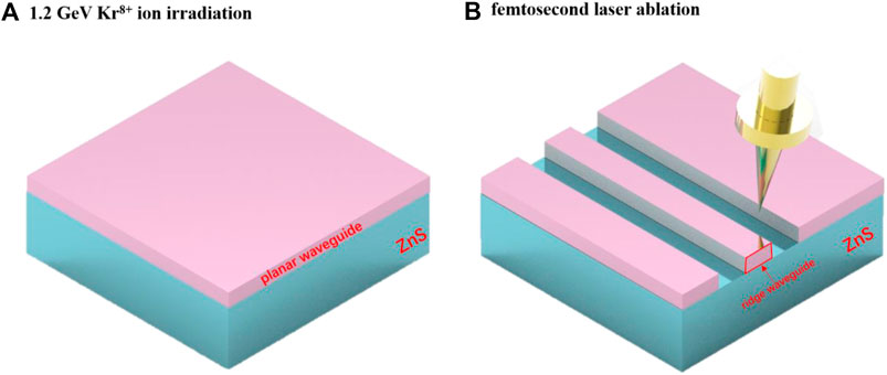
FIGURE 1. Preparation of ZnS ridge waveguides. (A) 1.2 GeV Kr8+ ion irradiation (B) femtosecond laser ablation.
Then, as shown in Figure 1B, we used a Titanium sapphire femtosecond laser system (FemtoYL™−25) at Shandong University to ablate two air grooves on the surface of the planar waveguide in ZnS crystal. The width of the waveguide is determined by the separation of the two adjacent air grooves. The minimal width of ridge waveguide can be provided with femtosecond laser ablation method is 20 µm. The femtosecond laser system produces a pulsed laser with a central wavelength of 1,031 nm, pulse width of 400 fs, a repetition frequency of 25,000 Hz, and maximum pulse energy of 7 mJ. The pulse laser energy is controlled at 15 μJ using a half-wave plate linear polarizer and a neutral density filter. The sample is placed on a three-dimensional motor stage, and the laser beam is focused on the sample surface through the objective lens (50 ×, N.A. = 0.67). The laser scanning speed is set at 0.1 mm/s, and two parallel grooves with depth of 115 μm are ablated to obtain a 40 µm wide ridge waveguide.
The cross-section of the ridge ZnS crystal waveguide was photographed with a metallographic microscope. The end face coupling system is arranged as shown in Figure 2. We used a laser source of a tunable laser system MIR™ 8025 to generate a mid-infrared incident light with a wavelength of 4 μm. The light beam is emitted from the light source, and after passing through a polarizer, it is focused into the ridge waveguide by the MIR objective lens Obj1. The light beam transmitted through the waveguide is converged by another MIR objective lens Obj2 and was observed by an MIR detector. We use MIR CCD to record the transmission mode of ZnS ridge waveguide, and use MIR optical power meter to measure the input power and output power of the ridge waveguide to calculate the propagation loss of the waveguide [29]. A cubic ZnSe glass placed between the polarizer and the objective lens Obj1 is used to adjust the incident angle of the beam, measure the maximum deflection angle of the waveguide, and calculate the maximum refractive index variation of the waveguide.
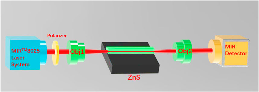
FIGURE 2. Schematic diagram of end face coupling system of ZnS crystal ridge optical waveguides.
In order to further reduce the propagation loss of the ridge waveguide, thermal annealing is performed on the ridge waveguide. We carried out four steps of annealing treatments, and the annealing temperatures were set as 180°C, 240°C, 300°C, 360°C successively, and the duration of each annealing was set 1 h. After each thermal annealing the ridge ZnS optical waveguide was placed in the end-face coupling system to measure input power and output power and calculate the propagation loss. Finally, in order to verify whether ion irradiation technology causes lattice damage of ZnS crystal, we measured Raman spectroscopy of the waveguide layer and substrate of ZnS crystal.
In order to study the ion deposition process in the ion irradiated region of the sample, we simulated the energy deposition process of 1.2 GeV Kr8+ ion irradiated ZnS by SRIM-2013. It can be seen from Figure 3A that in the range of 0–80 μm, the electronic stopping ability gradually increases from 10 keV/nm to 15 keV/nm, while the nuclear stopping ability is always zero. The nuclear stopping ability gradually increases from a depth of 80 μm and reaches a maximum of 1.5 keV/nm at 100 μm. We can conclude from the data that the electronic stopping ability plays a major role in the formation of waveguide.
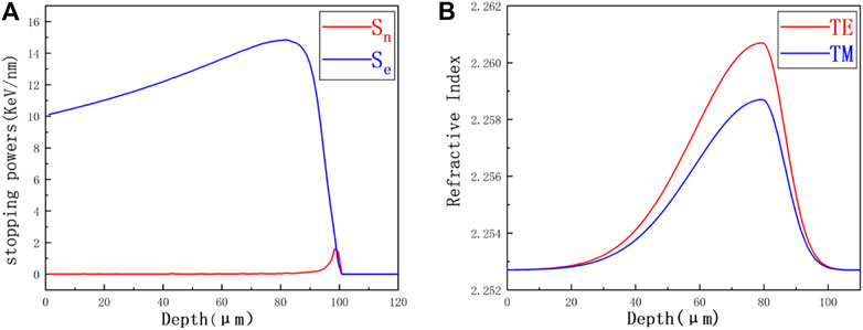
FIGURE 3. (A) Electron (blue line, Se) and nucleus (red line, Sn) stopping ability changes with the radiation depth of Kr8+ ions; (B) Refractive index curves of ZnS ridge waveguide at 4 μm wavelength in TM (blue line) and TE (red line) modes.
Due to the invisibility of the middle infrared light and the deep buried layer of the waveguide, it is impossible to measure the refractive index distribution by dark mode spectroscopy. In order to calculate the maximum refractive index change of the waveguide. Using the formula [30]:
Based on the end-face coupling system, the maximum light receiving angle θmTM = 9.9° in TM mode is measured. The maximum receiving angle of the waveguide in TE mode is θmTE = 10.9°. n = 2.2527 is the refractive index of ZnS crystal at the wavelength of 4 μm. We use Eq. 1 to calculate the maximum refractive index change in the waveguide region as ΔnTE = 0.008, ΔnTM = 0.006. An error of 30% is estimated due to uncertainty of the measured maximum incident angular deflection. Based on Δn and the curve of electron stopping ability, we reconstructed the refractive index distribution in the ZnS crystal waveguide region, as shown in Figure 3B. The maximum refractive index variation of TE mode is greater than that of TM mode, which indicates that the guiding properties at TE mode is better than TM mode.
As shown in Figure 4A, the photograph of cross section of the ridge ZnS crystal optical waveguide was taken by microscope, and the thickness of the waveguide layer is about 100 μm. Figures 4B,D show the experimental near-field mode distributions of TE and TM modes in the ZnS ridge optical waveguide at the wavelength of 4 μm obtained by the end-face coupling system. As we can see, both the near-field modal profiles of the waveguides at TE and TM modes exhibit multi-mode behaviors. On the basis of the reconstructed refractive index distribution, the finite-difference beam propagation method (FD-BPM) by RSoft software was used to simulate the near-field modal distribution of TE and TM modes in the ZnS ridge optical waveguide at the wavelength of 4 μm, as shown in Figures 4C,E. By comparing Figures 4B–E, we can see that the experimental and simulated modal profiles are consistent, which proves that the refraction index distribution reconstructed and simulation by Rsoft are correct. Thermal annealing treatment can eliminate the color centers and point defects of the waveguide, and reduce the degree of lattice damage, so as to reduce the propagation loss of the waveguide. As shown in Figure 5, the initial propagation loss of the ridge waveguide at TM mode was 2.9 dB/cm, and the propagation losses after annealing at 180°C, 240°C, 300°C, 360°C were reduced to 2.5 dB/cm, 1.9 dB/cm, 1.3 dB/cm, 0.8 dB/cm in turn, respectively. The initial propagation loss was 2.6 dB/cm at TE mode, and the propagation losses were reduced to 2.2 dB/cm 1.6 dB/cm 1.1 dB/cm 0.6 dB/cm after annealing at 180°C, 240°C, 300°C, 360°C, respectively. It can be seen that the propagation loss of ZnS ridge waveguide decreases with a series of annealing treatments, and the propagation loss of TE mode is lower than the TM mode with the same annealing treatment. This is because the maximum refractive index change of TE mode is larger than the TM mode, which has a stronger ability to constrain the transmission beam of waveguide and help to reduce the propagation loss of waveguide. After annealing, the propagation loss of the waveguide is further reduced, which indicates that thermal annealing is an effective method to further improve the guiding performance of the waveguides. Compared with previous reported ZnS waveguides by femtosecond laser ablation, the waveguide in our work has lower propagation loss [26].
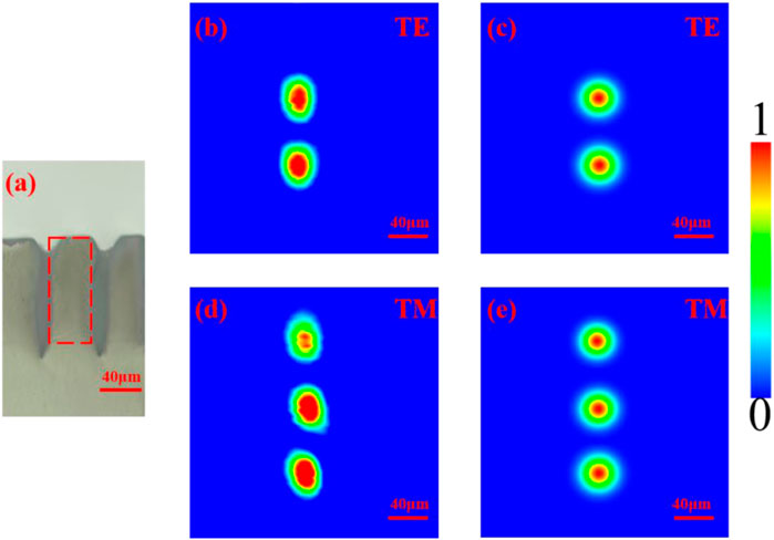
FIGURE 4. Microscopic images of ridge waveguides of ZnS crystals (A), experimental (B) and simulation (C) of near-field mode distribution of TE mode at 4 μm wavelength, experimental (D) and simulation (E) of near-field distribution in TM mode at 4 μm wavelength.
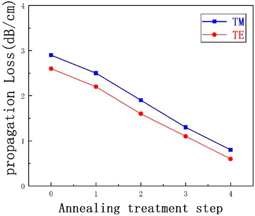
FIGURE 5. propagation loss of ZnS ridge waveguide in TM (blue line) and TE (red line) modes before and after annealing at 4 μm wavelength.
Figure 6 shows the Raman spectra of the ridge optical waveguide and the substrate in ZnS crystal. We can see that the Raman spectrum in the waveguide region is basically consistent with the substrate material, which proves that the ion irradiation does not cause large lattice damage to the material.
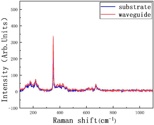
FIGURE 6. Raman spectra of 1.2 GeV Kr8+ ion irradiated ZnS crystal in waveguide region (blue line) and substrate region (red line).
We use ion irradiation combined with femtosecond laser ablation to fabricate ridge waveguide of ZnS crystal. The energy deposition process of ZnS crystal induced by ion irradiation is simulated by software. It is proved that the electron stopping ability plays an important role in the formation of waveguides. Based on the reconstructed refractive index distribution, the near-field light intensity distribution is in good agreement with the experimental results. The propagation losses of ridge waveguide in TE and TM modes are studied, and the thermal annealing technique is used to further optimize the ridge waveguide. The propagation loss at TE mode in the ridge waveguide of ZnS crystal is reduced to as low as 0.6 dB/cm at 4 μm wavelength after annealing. Raman spectroscopy shows that the ion irradiation does not cause large lattice damage to the crystal. Our experiment shows that the ZnS ridge waveguide manufactured by ion irradiation combined with femtosecond laser ablation method has a wide range of application prospects in mid-infrared integrated optics.
The raw data supporting the conclusion of this article will be made available by the authors, without undue reservation.
YC and XZ proposed the original idea and supervised the project. XZ performed the experiments and measurements and was responsible for writing the paper. YZ supported the formal analysis. All authors contributed to the article and approved the submitted version.
The work is supported by National Natural Science Foundation of China (NSFC) (No. 11805113), Natural Science Foundation of Guangdong Province (No. 2018A030313280), Project funded by China Postdoctoral Science Foundation (No. 2017M622192), Future Program for Young Scholars of Shandong University and Fundamental Research Funds of Shandong University.
The authors declare that the research was conducted in the absence of any commercial or financial relationships that could be construed as a potential conflict of interest.
All claims expressed in this article are solely those of the authors and do not necessarily represent those of their affiliated organizations, or those of the publisher, the editors and the reviewers. Any product that may be evaluated in this article, or claim that may be made by its manufacturer, is not guaranteed or endorsed by the publisher.
1. Zhu J, Zhu H, Xu H, Weng Z, Wu H. Ge-based Mid-infrared Blocked-Impurity-Band Photodetectors. Infrared Phys Technol (2018) 92:13–7. doi:10.1016/j.infrared.2018.04.015
2. Fuji T, Suzuki T. Generation of Sub-two-cycle Mid-infrared Pulses by Four-Wave Mixing through Filamentation in Air. Opt Lett (2007) 32(22):3330–2. doi:10.1364/OL.32.003330
3. Wu T, Kong W, Wang M, Wu Q, Chen W, Ye C, et al. Compact Hollow Waveguide Mid-infrared Gas Sensor for Simultaneous Measurements of Ambient CO2 and Water Vapor. J Lightwave Technol (2020) 38(16):4580–7. doi:10.1109/JLT.2020.2990977
4. Kasahara R, Kino S, Soyama S, Matsuura Y. Noninvasive Glucose Monitoring Using Mid-infrared Absorption Spectroscopy Based on a Few Wavenumbers. Biomed Opt Express (2018) 9(1):289–302. doi:10.1364/BOE.9.000289
5. Sales KC, Rosa F, Sampaio PN, Fonseca LP, Lopes MB, Calado CRC. In Situ Near-Infrared (NIR) versus High-Throughput Mid-infrared (MIR) Spectroscopy to Monitor Biopharmaceutical Production. Appl Spectrosc (2015) 69(6):760–72. doi:10.1366/14-07588
6. Hwang D, Ahn J, Hui K, Hui K, Son Y. Structural and Optical Properties of ZnS Thin Films Deposited by RF Magnetron Sputtering. Nanoscale Res Lett (2012) 7:26. doi:10.1186/1556-276X-7-26
7. Goudarzi A, Aval GM, Sahraei R, Ahmadpoor H. Ammonia-free Chemical bath Deposition of Nanocrystalline ZnS Thin Film Buffer Layer for Solar Cells. Thin Solid Films (2008) 516(15):4953–7. doi:10.1016/j.tsf.2007.09.051
8. Subbaiah YPV, Prathap P, Reddy KTR. Structural, Electrical and Optical Properties of ZnS Films Deposited by Close-Spaced Evaporation. Appl Surf Sci (2006) 253(5):2409–15. doi:10.1016/j.apsusc.2006.04.063
9. Shao L-X, Chang K-H, Hwang H-L. Zinc Sulfide Thin Films Deposited by RF Reactive Sputtering for Photovoltaic Applications. Appl Surf Sci (2003) 212-213(15):305–10. doi:10.1016/S0169-4332(03)00085-0
10. Zhang Z, Wang K, Zheng K, Deng S, Xu N, Chen J. Electron Bombardment Induced Photoconductivity and High Gain in a Flat Panel Photodetector Based on a ZnS Photoconductor and ZnO Nanowire Field Emitters. ACS Photon (2018) 5(10):4147–55. doi:10.1021/acsphotonics.8b00949
11. Wang X, Huang H, Liang B, Liu Z, Chen D, Shen G. ZnS Nanostructures: Synthesis, Properties, and Applications. Crit Rev Solid State Mater Sci (2013) 38(1):57–90. doi:10.1080/10408436.2012.736887
12. Wang K, Xub X, Ma L, Wang A, Wang R, Luo J, et al. Studies on Triboluminescence Emission Characteristics of Various Kinds of Bulk ZnS Crystals. J Lumin (2017) 186:307–11. doi:10.1016/j.jlumin.2017.02.006
13. Göde F, Gümüş C, Zor M. Investigations on the Physical Properties of the Polycrystalline ZnS Thin Films Deposited by the Chemical bath Deposition Method. J Cryst Growth (2007) 299(1):136–41. doi:10.1016/j.jcrysgro.2006.10.266
14. Carney DJ, Magnusson R. Ge-ZnS Mid-IR Wideband Resonant Reflectors. Proceedings of Frontiers in Optics 2017, OSA Technical Digest (online) (Optical Society of America, 2017 (2017) 62. doi:10.1364/FIO.2017.JW3A.62
15. Patel PC, Srivastava N, Srivastava PC. Synthesis of Wurtzite ZnS Nanocrystals at Low Temperature. J Mater Sci Mater Electron (2013) 24:4098–104. doi:10.1007/s10854-013-1367-z
16. Park W, King JS, Neff CW, Liddell C, Summers CJ. ZnS-Based Photonic Crystals. Phys Stat Sol (B) (2002) 229(2):949–60. doi:10.1002/1521-3951(200201)229:2<949::aid-pssb949>3.0.co;2-k
17. Chen C, Luan Q, He R, Cheng C, Akhmadaliev S, Zhou S, et al. Ridge Waveguides in Nd:ABC3O7 Disordered Crystals Produced by swift C5+ Ion Irradiation and Precise diamond Dicing: Broad Band Guidance and Spectroscopic Properties. Opt Laser Technol (2015) 68:84–8. doi:10.1016/j.optlastec.2014.11.017
18. Jia Y, Rüter CE, Akhmadaliev S, Zhou S, Chen F, Kip D. Ridge Waveguide Lasers in Nd:YAG Crystals Produced by Combining swift Heavy Ion Irradiation and Precise diamond Blade Dicing. Opt Mater Express (2013) 3(4):433–8. doi:10.1364/OME.3.000433
19. Grivas C. Optically Pumped Planar Waveguide Lasers, Part I: Fundamentals and Fabrication Techniques. Prog Quan Electron (2011) 35(6):159–239. doi:10.1016/j.pquantelec.2011.05.002
20. Yang Q, Liu H, Liu H, He S, Tian, Bin Xu Q, Wu P. Circular Cladding Waveguides in Pr:YAG Fabricated by Femtosecond Laser Inscription: Raman, Luminescence Properties and Guiding Performance. Opto-Electronic Adv (2021) 4(2):20000501–15. doi:10.29026/oea.2021.200005
21. Jia Y, Wang S, Wang S, Chen F. Femtosecond Laser Direct Writing of Flexibly Configured Waveguide Geometries in Optical Crystals: Fabrication and Application. Opto-Electronic Adv (2020) 3(10):190042. doi:10.29026/oea.2020.190042
22. Chen F. Micro- and Submicrometric Waveguiding Structures in Optical Crystals Produced by Ion Beams for Photonic Applications. Laser Photon Rev (2012) 6(5):622–40. doi:10.1002/lpor.201100037
23. Dong N, Yao Y, Chen F. Optical Waveguides in Nd:GdVO4 Crystals Fabricated by swift N3+ Ion Irradiation. Opt Mater (2012) 35(2):310–3. doi:10.1016/j.optmat.2012.09.024
24. Jia C-L, Wang X-L, Wang K-M, Ma H-J, Nie R. Characterization of Optical Waveguide in Nd: GdVO4 by Triple-Energy Oxygen Ion Implantation. Appl Surf Sci (2007) 253(24):9311–4. doi:10.1016/j.apsusc.2007.05.064
25. Salleh S, Dalimin MN, Rutt HN. The Propagation Losses of Cold Deposited Zinc Sulfide Waveguides. Amr (2011) 216:332–6. doi:10.4028/www.scientific.net/amr.216.332
26. An Q, Ren Y, Jia Y, Vázquez de Aldana JR, Chen F. Mid-infrared Waveguides in Zinc Sulfide crystal. Opt Mater Express (2013) 3(4):466–71. doi:10.1364/OME.3.000466
27. Liu T, Kong W-J, Qiao M, Cheng Y. Maintain Raman Property in ZnS Single crystal Waveguide Formed by Multi-Energy He Ion Implantation at 633 nm. Results Phys (2018) 11:822–5. doi:10.1016/j.rinp.2018.10.031
28. Liu T, Yao Y-C, Liu F-R, Cheng L, Bao Y-F, Kong W-J, et al. Enhanced Raman Intensity in ZnS Planar and Channel Waveguide Structures via Carbon Ion Implantation. Opt Mater (2021) 112:110733. doi:10.1016/j.optmat.2020.110733
29. Wang L, Chen F, Wang X-L, Wang K-M, Jiao Y, Wang L-L, et al. Low-loss Planar and Stripe Waveguides in Nd3+-Doped Silicate Glass Produced by Oxygen-Ion Implantation. J Appl Phys (2007) 101(5):053112. doi:10.1063/1.2710293
Keywords: optical waveguide, femtosecond laser ablation, ZnS crystal, ion irradiation, mid-infrared
Citation: Zhang X, Cheng Y and Zhang Y (2021) Mid-Infrared ZnS Ridge Waveguide Fabricated by Femtosecond Laser Ablation Combined With Ion Irradiation. Front. Phys. 9:731571. doi: 10.3389/fphy.2021.731571
Received: 27 June 2021; Accepted: 14 July 2021;
Published: 30 July 2021.
Edited by:
Hongliang Liu, Nankai University, ChinaReviewed by:
Jinhua Zhao, Shandong Jianzhu University, ChinaCopyright © 2021 Zhang, Cheng and Zhang. This is an open-access article distributed under the terms of the Creative Commons Attribution License (CC BY). The use, distribution or reproduction in other forums is permitted, provided the original author(s) and the copyright owner(s) are credited and that the original publication in this journal is cited, in accordance with accepted academic practice. No use, distribution or reproduction is permitted which does not comply with these terms.
*Correspondence: Yazhou Cheng, Y2hlbmd5YXpob3VAc2R1LmVkdS5jbg==; Yongcheng Zhang, cWR6aHljQHFkdS5lZHUuY24=
Disclaimer: All claims expressed in this article are solely those of the authors and do not necessarily represent those of their affiliated organizations, or those of the publisher, the editors and the reviewers. Any product that may be evaluated in this article or claim that may be made by its manufacturer is not guaranteed or endorsed by the publisher.
Research integrity at Frontiers
Learn more about the work of our research integrity team to safeguard the quality of each article we publish.