 Daijing Xu
 Shubin Yan
 Xiaoyu Yang1,2
94% of researchers rate our articles as excellent or good
Learn more about the work of our research integrity team to safeguard the quality of each article we publish.
Find out more
ORIGINAL RESEARCH article
Front. Phys. , 18 August 2021
Sec. Optics and Photonics
Volume 9 - 2021 | https://doi.org/10.3389/fphy.2021.702193
Optical devices play an important role in different fields, such as refractive index detection in food processing and the biochemical industry. In our work, a novel nanoscale optical structure, composed of a metal-insulator-metal waveguide with a stub and a horizontal number eight-shape cavity (HNEC), is presented. The transmission properties of this structure are investigated in detail by using finite element method The effects of geometric parameters on sensing performance are studied in detail. Moreover, the influences of an asymmetric resonator caused by shifting central rectangular cavity of HNEC on transmission spectrum are discussed. The changing parameters of HNEC resonator have different effects on different resonance dips. Then, when the parameters of this presented structure are fixed as a of 540 nm, b of 340 nm, S of 0, l of 70 nm and g of 10 nm, this intriguing structure can serve as a refractive index sensor, whose maximum sensitivity can reach 1,500 nm/refractive index unit with a figure of merit of 75. Therefore, this structure will contribute to the development of miniaturization of optical devices.
Surface plasmon polaritons (SPPs) are electromagnetic waves that can be considered as the energy and optical signal carrier in next-generation ultrahigh-density integrated photonic circuits because they can overcome the traditional diffraction limit [1–3]. Furthermore, SPPs also show a promising pathway for realization of the high-sensitivity nano-sensor because of their strong field confinement and the surface field enhancement at the interface of the metal and dielectric [4–6]. In recent years, numerous SPP guiding structures have been systematically discussed, such as metal-insulator-metal (MIM) waveguides, nano-slits, hybrid Bragg waveguides, metal nanoparticle waveguides, and plasmonic nanoclusters. Among these, the MIM waveguides are considered as the preferable structure as a result of its strong deep-subwavelength confinement, easy integration, and low bend loss. Therefore, many kinds of optical devices based on the MIM waveguide coupled with resonator are investigated, including nanosensors [7–13], demultiplexers [14], optical switch [15, 16], filters [17–19], logic gate [20], and so on. These devices can be applied in future optical on-chip nanodevices.
An intriguing physical feature based on Fano resonance has been found. Fano resonance has great potential in sensing fields owing to their comparatively high sensitivity and figure of merit (FOM) [21]. This phenomenon arises from the coherent interference between bright mode and dark mode. Its transmission spectrum shows a sharp and asymmetric profile [7, 22]. In the last few years, many works about the structure of the MIM waveguide coupled with a resonator which can generate Fano resonance have been produced. A nano-sensor was designed by Zhang et al. [7] consisting of MIM waveguide and double rectangular cavity, which achieved 596 nm/RIU. Zhang et al. [8] designed a refractive index sensor with a sensitivity of 1,160 nm/RIU (refractive index unit), which was comprised of MIM waveguide and dual side-coupled ring resonators. Li et al. [9] proposed a nanostructure with multiple rectangular cavities based on MIM waveguide system which can reach 1,011 nm/RIU with FOM of 47.91. Zhu and Li [10] presented a structure of MIM waveguide coupled with a semicircular resonator and a key-shape resonator, which can reach 1,261.67 nm/RIU. Rakhshani [23] designed a structure with circular arrays of nanorods and nanotubes for detecting cancerous cells, whose maximum FOM and sensitivity are 19.5 and 1,055 nm/RIU, respectively. Rakhshani [24] also proposed a structure using nanorods array for imaging, which can reach 1,200 nm/RIU. However, the problem of sensing performance hinders the development of integrated optical circuits. Thus, how to improve the value of FOM or sensitivity is a key task for future research works.
In our work, a nanostructure composed of MIM waveguide with a stub and a Horizontal Number Eight-Shape cavity (HNEC) is designed. Furthermore, the model of proposed structure is numerically analyzed by the finite element method. Here, the formation reason of Fano resonance in our proposed structure is investigated according to the transmission spectra and the magnetic field distribution. Meanwhile, the effects of geometric parameters of this structure on sensing performance are analyzed in detail. Additionally, the influences of asymmetric resonator caused by shifting central rectangular cavity of HNEC on transmission spectrum are studied. Finally, the application of the designed structure is discussed, which has a sensitivity of 1,500 nm/RIU and an FOM of 75. It has great potential for use in refractive index nano-sensors. The sensing performance of the proposed structure is better than those mentioned above. In addition, compared with other MIM-based structures with high sensing performance not listed, this structure has a smaller size in the case of small performance gap. It can also be integrated easily. This proposed structure makes it easier for fabrication in the future. Hence, it will play an important role in the high-density integrated optical circuit in the future.
Figure 1 displays 2D and 3D schematics of the proposed structure, comprising a MIM waveguide with a stub and a HNEC resonator. As shown in Figure 1B, this structure is built on the SiO2 substrate. The blue part and white part in Figure 1 represent Ag and air, respectively. Silver is selected as the metal material for MIM waveguide because of the lower power-consumption. Compared with gold (Au), Ag has merit due to its lower absorption and lower ohmic loss to guarantee a stronger field intensity, which promotes the propagation properties. The length of the HNEC is a and the width of the HNEC is b.g denotes the coupling distance between the HNEC resonator and the stub resonator, and l denotes the height of the stub resonator. Meanwhile, to ensure that only the transverse magnetic mode (TM) is propagated in this designed structure, the width of the HNEC resonator, stub, and bus waveguide are w = 50 nm. S represents horizontal shift distance of central rectangular cavity. When S = 0 nm, the structure is in symmetry with the reference line. In our work, the model of this structure is simulated by using COMSOL Multiphysics 5.4a. The incident light enters this structure from input port Pi and excites SPPs, which propagate through the bus waveguide and couple into the stub resonator and HNEC resonator. Finally, it will output from the port Po. The transmittance of this system can be described as T = |Po|2/|Pi|2.
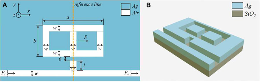
FIGURE 1. (A) 2D schematic of the proposed structure. (B) 3D schematic diagram of the designed structure.
The complex relative permittivity ε(w) of silver is described by the well-known Drude dispersion model [25]:
where ε∞= 3.7, γ = 0.018 ev, and ωp = 9.1ev. It agrees well with the experiment value [26] in the range of 800∼2000 nm.
The TM mode equation of MIM waveguides is expressed as [27, 28]:
where w denotes the width of waveguide and k is wave vector in the waveguide. αc = [k02 (εin - εm) + k]1/2, p = εin/εm. The k0 = 2π/λ0 is the wave vector in free space. The εm and εin are permittivity of metal and dielectric, respectively. According to (Eqs. 1, 2), the real part of refractive index Re (neff) can be obtained by Re (neff) = [ εm+ (k/k0)2]1/2. k can be calculated by equation (Equ. 2) using iterative method.
Resonance would occur in this structure when the phase-match condition is satisfied. According to the standing wave theory, the resonance wavelength (λr) can be described as [8, 29, 30]:
where k can be solved by Equation 1 and mode order is m, which can be calculated by m = 2L/λspp.L is the effective length of resonator. λspp is the wavelength of SPPs and it can be expressed as λspp = λ0/Re(neff). Re (neff) is the real part of effective refractive-index and φref is the phase shift of SPP reflection at the cavity metal wall.
To evaluate the sensing performance of the designed structure, two important evaluation indices should be considered, including the sensitivity (Sr) and FOM. They can be described as [31]:
where ∆λ and ∆n are the variation of resonance wavelength and change of refractive indices, respectively. FWHM is full width at half maximum of resonant peak/dip.
To understand the transmission properties of the presented structure and the formation process of Fano resonance, the transmission spectra of waveguide with the HNEC resonator, waveguide with the stub resonator, and prototype structure are investigated respectively. The initial geometric values of the prototype structure are fixed as g = 10 nm, l = 70 nm, a = 540 nm, b = 320 nm, and S = 0 nm. The transmission spectrum of the prototype structure exhibits two fano resonances at 1,177 nm (R2) and 1,469 nm (R1) as shown in Figure 2, and it shows an asymmetric and sharp outline. This phenomenon can be explained by the interaction of bright mode (broad continuous state) and dark mode (sharp discrete state). For the black curve, the broad continuous outline, transmittance changes slowly in the range of 0.7–1.0. Additionally, the stub resonator is directly excited by the SPPs generated from the input port. Therefore, the transmittance will remain at a relatively high value, which can be called the bright mode. For the blue curve, the transmission spectrum of the waveguide with the HNEC resonator displays some dips, which are next to R1 and R2, with extremely low transmittance. Further, the HNEC resonator is directly excited by the stub resonator instead of the bus waveguide. Thus, the HNEC resonator acts as a dark resonator (dark mode).
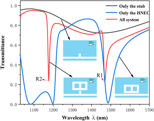
FIGURE 2. Transmission spectra of the waveguide with the HNEC resonator (blue line), waveguide with stub resonator (black line), and prototype structure (red line).
Successively, to further explore the transmission characteristics of the prototype structure, the magnetic field Hz distributions of this structure are investigated. As depicted in Figure 3, when incident wavelengths are at R1 and R2, most of the magnetic field is concentrated in HNEC resonator. When the incident wavelength λ = 1,469 nm, the effective length L = 2 (a-w) + 3 (b-w) = 1790 nm, according to Eqs 1–3, the effective index neff≈ 1.377–0.003i, and the propagation length of SPPs Lspp≈ 1/(2kspp) = 1/{2k0 [εm× εin/(εm+εin)]1/2} ≈ 32 μm. This total length of this designed structure, at about 3 μm, is much smaller than the propagation length of SPPs. Hence, the Ohmic loss in the metal can be neglected. The effective SPPs wavelength λspp can be calculated by λspp= λ/Re (neff) ≈ 1,067 nm. Hence, the mode order can be calculated by m = 2L/λspp≈ 3.36 = 3. In a similar way, when the incident wavelength λ = 1,177 nm, λspp= λ/Re (neff) = 841 nm, and the mode order can be calculated by m = 2L/λspp≈ 4.26 = 4. It is consistent with the simulation results in Figure 3. On the contrary, when we know the value of mode order, the resonant wavelength can be calculated. It indicates that the HNEC resonator has strong ability to trap the SPPs, resulting in a lower transmittance in the spectrum. However, there are some different characteristics in resonance R1 and R2. First, when the incident wavelength is at R2, as plotted in Figure 3A, there are four nodes in the HNEC resonator. The Hz field is divided into three parts, two of which are concentrated on the ends of the HNEC resonator. However, when wavelength is at R1, there are three nodes in the HNEC resonator, as shown in Figure 3B. The Hz field is divided into two parts, which are concentrated on the upper parts and lower parts of the HNEC resonator. Second, as shown in Figure 2, it can be seen that the FWHM of R2 is narrower than that of R1. Third, after calculating the sensitivity of the two dips in prototype structure (this will be calculated in the discussion below), the sensitivity of R1 is 1,423 nm/RIU and that of R2 is 1,162 nm/RIU. These phenomena show that the resonance caused by different incident wavelengths have different sensing performances. According to Eqs 3–6, the change of resonance wavelength will make the dip in the different resonance mode, which has a great relationship with the sensing performance of the presented structure.
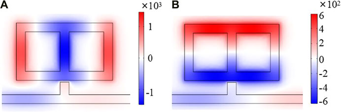
FIGURE 3. The Hz field distribution at (A)λ = 1,177 nm (R2), (B)λ = 1,469 nm (R1).
Subsequently, the influences of geometric parameters of this prototype structure on sensing performance are studied. The impact of the length a of HNEC resonator is examined. The value of a changes from 520 to 560 nm at intervals of 10 nm and other parameters of this structure remain the same. The resonance R1 and R2 have evident redshift with increasing a as plotted in Figure 4A. According to equation (3), the resonance wavelength will red shift with the increase of the effective length of the HNEC resonator by increasing a. Additionally, the transmittance of R2 increases with the increase of a but that of R1 has no obvious change. It can be inferred that the R2 is more susceptible to the changes of geometric parameters. Figures 4B,C show the fitting curve of sensitivity at different resonance dips. For the R2, the maximum and minimum sensitivity are 1,174 nm/RIU and 1,137 nm/RIU, respectively. For the R1, the maximum and minimum sensitivity are 1,477 nm/RIU and 1,386 nm/RIU, respectively. Moreover, the change of sensitivity at R1 when increasing the a is more obvious than that of R2. Therefore, the dip R1 is more suitable to act as a nanosensor than dip R2.
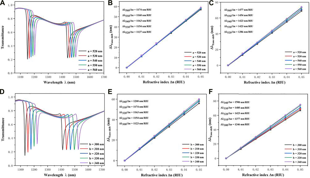
FIGURE 4. (A) transmission spectra for different a of HNEC; fitting curve of sensitivity (B) at R2; (C) at R1; (D) transmission spectra for different b of HNEC; fitting curve of sensitivity (E) at R2; (F) at R1.
Similarly, the effects of the width b of HNEC resonator are then investigated. The parameter b increases from 300 to 340 nm at intervals of 10 nm and other parameters of this structure stay the same. The resonance dips have obvious red shift with the increase of parameter b in Figure 4D. The reason for this phenomenon is the same as the explanation of parameter a mentioned above. When increasing b, the transmittance of dip R2 increases remarkably and that of dip R1 still has no obvious change. The sensitivity of dip R1 and R2 increase remarkably with the increase of parameter b in Figures 4E,F. It is indicated that the transmission properties are mainly determined by the parameter b. In other words, b is a key parameter in the presented structure, which can be applied in tuning the sensing performance of this structure to meet individual requirements.
The remaining geometrical parameters of HNEC are investigated, including parameter l and parameter g. Transmission spectra for different l is shown in Figure 5A, which increases from 50 to 90 nm at intervals of 10 nm. Meanwhile, other parameters remain unchanged. When l increases, the resonance wavelength and the transmittance of R1 and R2 stay the same. It is indicated that transmission properties are almost unaffected by the height of the stub resonator. Moreover, after calculating FWHM and the sensitivity, two evaluation indices also lack obvious changes when increasing l. It can be seen that l is not an important parameter for this structure. However, for coupling distance g, the transmission spectra have changed dramatically, as shown in Figure 5B. It is seen from Figure 5B that the transmittance of R1 and R2 increases sharply with the increase of coupling distance. It can be explained by the theory that the ability of coupling SPPs into HNEC resonator becomes weaker with increasing g. Furthermore, Figure 5C shows that the FWHM of R1 and R2 decreases with the increase of g. When the coupling distance is equal to 10 nm, the values of transmittance and FWHM are in good condition. Therefore, the coupling distance g = 10 nm is more suitable for the presented structure.
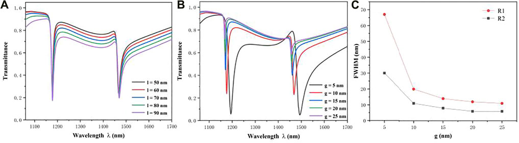
FIGURE 5. (A) Transmission spectra for changing l of HNEC resonator; (B) transmission spectra for changing g of HNEC resonator; (C) the value of FWHM for the increase of g.
In this paper, the influences of asymmetry of the HNEC resonator on the transmission properties are also investigated. Six derived structures obtained by shifting the central rectangular cavity of HNEC resonator are discussed. The displacement distances S of the derived structures are set as −50, −100, −150, 50, 100, and 150 nm, respectively. The other parameters are still fixed as a of 540 nm, b of 320 nm, l of 70 nm, and g of 10 nm. In order to describe this easily, the derived structures are divided into three groups. Group 1 is composed of the structure with S = 150 nm and structure with S = −150 nm. Group 2 is composed of the structure with S = 100 nm and structure with S = −100 nm. Group 3 is composed of the structure with S = 50 nm and structure with S = −50 nm. As shown in Figure 6A, structures in the same group have similar transmission spectrums. It can be inferred that two structures that are in symmetry with the reference line have similar transmission properties. Therefore, the structures with S = 0 nm, S = 50 nm, S = 100 nm, and S = 150 nm are then investigated. There are two intriguing phenomena in Figure 6A. First, when S gradually increases, R1 has red shifts, while R2 has blue shifts. To easily explain this phenomenon, as shown in Figure 6B, we assumed that the larger rectangle right above the stub resonator is the Rect 1 and another smaller one is Rect 2. It can be seen from the above discussion that movement of resonance dip is related to the effective length of the resonator. Therefore, it can be inferred that R1 is mainly affected by Rect 1 and R2 is mainly affected by Rect 2. As a result, the R1 has red shifts and the R2 has blue shifts when S gradually increases. Second, for R2, the transmittance of resonance dip obviously decreases with the increase of S. However, for R1, the transmittance of resonance dip has no obvious variation trend. It is indicated that the ability of trapping SPPs for R2 is enhanced with the change of S. To further explain the reason of this phenomenon, the Hz field distributions of the structure with S = 0 nm, S = 50 nm, S = 100 nm, and S = 150 nm at R2 are studied. As shown in Figures 7A–D, when S = 0 nm, the magnetic field distribution at both ends of the HNEC resonator are similar, and the magnetic field mainly concentrates on the central rectangle cavity. Meanwhile, the Hz field is in symmetry with the reference line. However, when increasing S, the Hz field intensity of the leftmost rectangle becomes gradually weaker and stronger in the rightmost rectangle cavity. The distribution of magnetic field becomes asymmetric due to the asymmetric structure. Moreover, the power flow at ends of the HNEC resonator is difficult to leak into the bus waveguide. Therefore, the transmittance of R2 gradually decreases with the increase of S. However, for R1, as shown in Figures 7E–G, the Hz field is always distributed in the upper and lower part of the HNEC resonator. The power flow leakage leads to similar transmittance of resonance dip. Meanwhile, due to the influence of the Hz field, the corresponding electric field distributions are shown in Figure 8.
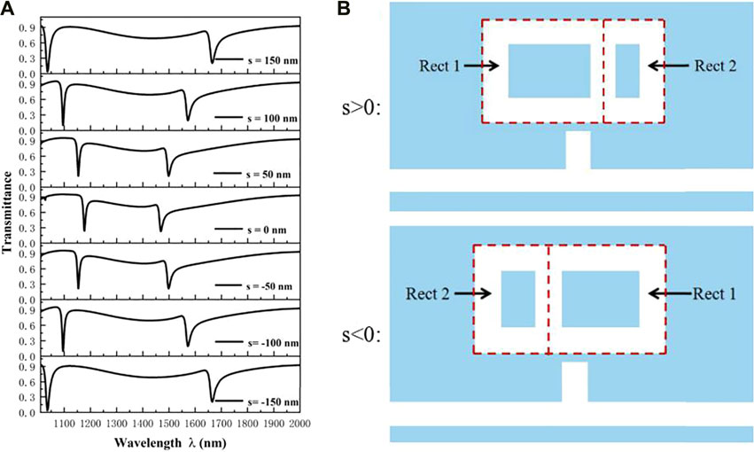
FIGURE 6. (A) Transmission spectra for changing displacement distance. (B) schematic of defining Rect one and Rect two.
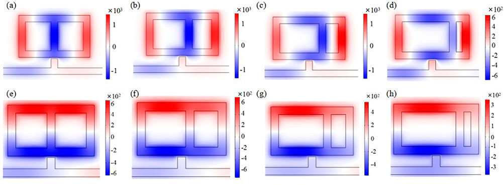
FIGURE 7. The Hz field distribution of structure with (A)S = 0 nm; (B)S = 50 nm; (C)S = 100 nm; (D)S = 150 nm at R2. the Hz field distribution of structure with (E)S = 0 nm; (F)S = 50 nm; (G)S = 100 nm; (H)S = 150 nm at R1.
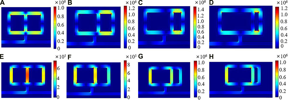
FIGURE 8. The electric field distribution of structure with (A)S = 0 nm; (B)S = 50 nm; (C)S = 100 nm; (D)S = 150 nm at R2. the Hz field distribution of structure with (E)S = 0 nm; (F)S = 50 nm; (G)S = 100 nm; (H)S = 150 nm at R1.
The structure, whose parameters are fixed as a = 540 nm, b = 340 nm, g = 10 nm, l = 70 nm, and S = 0 nm, served as the refractive index sensor in the following discussion according to the influence of structure parameters on sensing performance. From the conclusion of the above paragraphs, the sensing performance of R1 is better than that of R2. Therefore, R1 is considered as the appropriate resonance dip for the detection. Based on this structure’s parameters just mentioned, R1 of the presented structure can obtain its best performance whose sensitivity is 1,500 nm/RIU with a FOM of 75. Table 1 shows comparisons of results with some reported research [32–34] on structure type, sensing performance, and wavelength range in recent years. As shown in Figure 9, the dips exhibit linear redshift. That is to say, the refractive index can be obtained by the value of R1 when this structure serves as the refractive-index sensor. The fabrication of this structure can be realized by the focused iron beam on a 100 nm thick Ag film that is sputtered on a quartz substrate [35, 36]. Additionally, another way to fabricate the proposed structure is to deposit a thin layer of Ag on a quartz substrate and then etch the silver film. Specifically, the Ag film is deposited on a quartz substrate followed by a spin coating of an electron-sensitive film (resist). The custom shapes on a resist can be fabricated by using E-beam lithography. Then, to obtain the desirable pattern, wet etching can be used to remove the undesirable Ag. Finally, the resist is removed [37]. The nanofiber is connected to input port as an incident channel for light source. Meanwhile, the output signal will be detected by JY Confocal Raman Microscopy that is connected to output port [38].

TABLE 1. comparisons of some reported research.
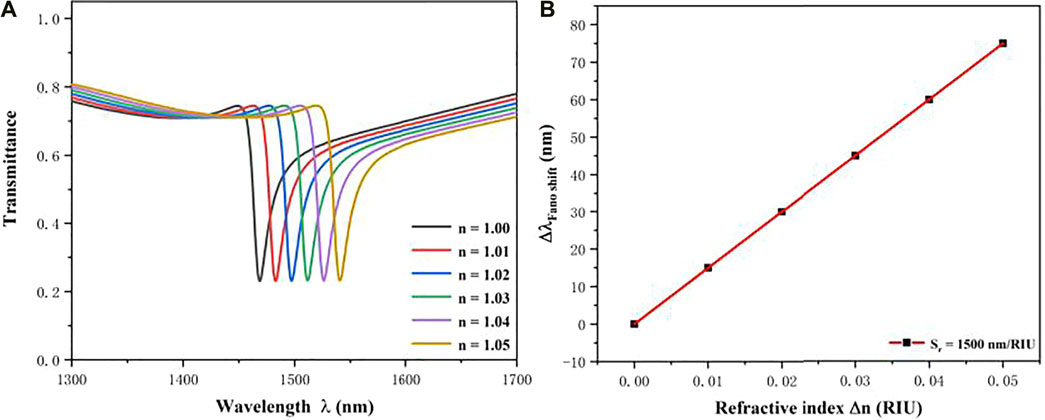
FIGURE 9. (A) transmission spectra for variable n; (B) fit curve of sensitivity at R1.
Additionally, physical quantities linearly related to the refractive index can also be measured. For example, it can be used as biochemical sensors in glucose concentration detection. Changes in concentration of the glucose solution have influence on the refractive index of the solution. So, when we get the value of refractive index by detecting the resonance dip, the corresponding concentration of glucose solution can be calculated. The glucose solution can be loaded into this structure by capillary attraction [39]. The relationship between refractive index and glucose concentration is described in detail in Refs. [10, 40]:
where C is the glucose concentration (g/L) and n is the refractive index. According to the Equation 6, the corresponding concentration value can be calculated when the refractive index is measured.
In summary, a novel nanostructrue is proposed in this paper, which consists of waveguide with a stub and a horizontal number eight-shape cavity. It has great advantages in the application of a refractive index nanosensor and other biochemical nanosensors. When the parameters of this presented structure are fixed as a of 540 nm, b of 340 nm, S of 0, l of 70 nm, and g of 10 nm, the maximum sensitivity of 1,500 nm/RIU and FOM of 75 can be obtained. There are two research results in this paper. On the one hand, the sensing performance can be adjusted by changing the structure parameters. The parameter b plays a vital role in adjusting sensitivity of this proposed structure. Moreover, the parameter g is a key parameter in changing the transmittance and FWHM. Compared with b and g, the parameter a and parameter l have little influence on the sensing performance of this structure. On the other hand, the asymmetric resonator caused by the shifting central rectangular cavity of HNEC resonator has different effects on different resonance dips. The transmission properties of R1 are mainly affected by Rect 1 and that of R2 are mainly affected by Rect 2. Therefore, our work is significant for the development of optical on-chip nanodevices. Meanwhile, this study also has reference significance for other researchers in the design of high-performance optical nanostructures.
The original contributions presented in the study are included in the article/Supplementary Material, further inquiries can be directed to the corresponding authors.
DX wrote the manuscript and carried out the simulation. SY conceived and designed the simulation. XY, JW, and XW designed the pictures and performed the simulation. EH revised the manuscript.
This work was supported by the National Natural Science Foundation of China (Grant number 61675185, 61875250, 61975189), The Zhejiang Provincial Natural Science Foundation of China (Grant number LD21F050001), the Key Research and Development Project of Zhejiang Province (Grant number 2021C03019), and Shanxi 1,331 Project Key Subject Construction.
The authors declare that the research was conducted in the absence of any commercial or financial relationships that could be construed as a potential conflict of interest.
All claims expressed in this article are solely those of the authors and do not necessarily represent those of their affiliated organizations, or those of the publisher, the editors and the reviewers. Any product that may be evaluated in this article, or claim that may be made by its manufacturer, is not guaranteed or endorsed by the publisher.
The authors are thankful to other colleagues in their laboratory for their understanding and help.
1. Barnes WL, Dereux A, Ebbesen TW. Surface Plasmon Subwavelength Optics. Nature (2003) 424:824–30. doi:10.1038/nature01937
2. Gramotnev DK, Bozhevolnyi SI. Plasmonics Beyond the Diffraction Limit. Nat Photon (2010) 4:83–91. doi:10.1038/nphoton.2009.282
3. Yin Y, Qiu T, Li J, Chu PK. Plasmonic Nano-Lasers. Nano Energy (2012) 1:25–41. doi:10.1016/j.nanoen.2011.09.002
5. Han Z, Bozhevolnyi SI. Radiation Guiding With Surface Plasmon Polaritons. Rep Prog Phys (2013) 76:016402. doi:10.1088/0034-4885/76/1/016402
6. Zayats AV, Smolyaninov II, Maradudin AA. Nano-Optics of Surface Plasmon Polaritons. Phys Rep (2005) 408:131–314. doi:10.1016/j.physrep.2004.11.001
7. Zhang Z, Luo L, Xue C, Zhang W, Yan S. Fano Resonance Based on Metal-Insulator-Metal Waveguide-Coupled Double Rectangular Cavities for Plasmonic Nanosensors. Sensors (2016) 16:642. doi:10.3390/s16050642
8. Zhang X, Qi Y, Zhou P, Gong H, Hu B, Yan C. Refractive Index Sensor Based on Fano Resonances in Plasmonic Waveguide With Dual Side-Coupled Ring Resonators. Photonic Sens (2018) 8:367–74. doi:10.1007/s13320-018-0509-6
9. Li Z, Wen K, Chen L, Lei L, Zhou J, Zhou D. Control of Multiple Fano Resonances Based on a Subwavelength MIM Coupled Cavities System. IEEE Access (2019) 7:59369–75. doi:10.1109/ACCESS.2019.2914466
10. Zhu J, Li N. MIM Waveguide Structure Consisting of a Semicircular Resonant Cavity Coupled With a Key-Shaped Resonant Cavity. Opt Express (2020) 28:19978–87. doi:10.1364/OE.395696
11. Rakhshani MR, Mansouri-Birjandi MA. Engineering Hexagonal Array of Nanoholes for High Sensitivity Biosensor and Application for Human Blood Group Detection. IEEE Trans Nanotechnology (2018) 17:475–81. doi:10.1109/TNANO.2018.2811800
12. Rakhshani MR, Mansouri-Birjandi MA. Utilizing the Metallic Nano-Rods in Hexagonal Configuration to Enhance Sensitivity of the Plasmonic Racetrack Resonator in Sensing Application. Plasmonics (2016) 12:999–1006. doi:10.1007/s11468-016-0351-x
13. Rakhshani MR, Mansouri-Birjandi MA. High-Sensitivity Plasmonic Sensor Based on Metal-Insulator-Metal Waveguide and Hexagonal-Ring Cavity. IEEE Sensors J (2016) 16:3041–6. doi:10.1109/JSEN.2016.2522560
14. Hu F, Yi H, Zhou Z. Wavelength Demultiplexing Structure Based on Arrayed Plasmonic Slot Cavities. Opt Lett (2011) 36:1500. doi:10.1364/OL.36.001500
15. Tao J, Wang QJ, Huang XG. All-Optical Plasmonic Switches Based on Coupled Nano-Disk Cavity Structures Containing Nonlinear Material. Plasmonics (2011) 6:753–9. doi:10.1007/s11468-011-9260-1
16. Bazgir M, Jalalpour M, Zarrabi FB, Arezoomand AS. Design of an Optical Switch and Sensor Based on a MIM Coupled Waveguide Using a DNA Composite. J Elec Materi (2020) 49:2173–8. doi:10.1007/s11664-019-07902-3
17. Chen L, Lu P, Tian M, Liu D, Zhang J. A Subwavelength MIM Waveguide Filter With Single-Cavity and Multi-Cavity Structures. Optik - Int J Light Electron Opt (2013) 124:3701–4. doi:10.1016/j.ijleo.2012.11.025
18. Zheng G, Su W, Chen Y, Zhang C, Lai M, Liu Y. Band-Stop Filters Based on a Coupled Circular Ring Metal-Insulator-Metal Resonator Containing Nonlinear Material. J Opt (2012) 14:055001–6. doi:10.1088/2040-8978/14/5/055001
19. Hocini A, Ben salah H, Khedrouche D, Melouki N. A High-Sensitive Sensor and Band-Stop Filter Based on Intersected Double Ring Resonators in Metal-Insulator-Metal Structure. Opt Quant Electron (2020) 52:52. doi:10.1007/s11082-020-02446-x
20. Akhlaghi M, Kaboli M. Investigating the Optical XNOR Gate Using Plasmonic Nano-Rods. Photon Nanostructures - Fundamentals Appl (2016) 19:24–30. doi:10.1016/j.photonics.2016.02.001
21. Miroshnichenko AE, Flach S, Kivshar YS. Fano Resonances in Nanoscale Structures. Rev Mod Phys (2010) 82:2257–98. doi:10.1103/RevModPhys.82.2257
22. Pang S, Huo Y, Xie Y, Hao L. Fano Resonance in MIM Waveguide Structure With Oblique Rectangular Cavity and its Application in Sensor. Opt Commun (2016) 381:409–13. doi:10.1016/j.optcom.2016.07.052
23. Rakhshani MR. Tunable and Sensitive Refractive Index Sensors by Plasmonic Absorbers With Circular Arrays of Nanorods and Nanotubes for Detecting Cancerous Cells. Plasmonics (2020) 15:2071–80. doi:10.1007/s11468-020-01237-0
24. Rakhshani MR. Three-Dimensional Polarization-Insensitive Perfect Absorber Using Nanorods Array for Sensing and Imaging. IEEE Sensors J (2020) 20:14166–72. doi:10.1109/JSEN.2020.3008489
25. Lu H, Liu X, Mao D, Gong Y, Wang G. Induced Transparency in Nanoscale Plasmonic Resonator Systems. Opt Lett (2011) 36:3233–5. doi:10.1364/OL.36.003233
26. Johnson PB, Christy RW. Optical Constants of the noble Metals. Phys Rev B (1972) 6:4370–9. doi:10.1103/physrevb.6.4370
27. Dionne JA, Sweatlock LA, Atwater HA, Polman A. Plasmon Slot Waveguides: Towards Chip-Scale Propagation With Subwavelength-Scale Localization. Phys Rev B (2006) 73:035407. doi:10.1103/PhysRevB.73.035407
28. Kekatpure RD, Hryciw AC, Barnard ES, Brongersma ML. Solving Dielectric and Plasmonic Waveguide Dispersion Relations on a Pocket Calculator. Opt Express (2009) 17:24112–29. doi:10.1364/OE.17.024112
29. Chen L, Liu Y, Yu Z, Wu D, Ma R, Zhang Y. Numerical Analysis of a Near-Infrared Plasmonic Refractive Index Sensor With High Figure of Merit Based on a Fillet Cavity. Opt Express (2016) 24:9975–83. doi:10.1364/OE.24.009975
30. Zhu JH, Wang QJ, Shum P, Huang XG. A Simple Nanometeric Plasmonic Narrow-Band Filter Structure Based on Metal-Insulator-Metal Waveguide. IEEE Trans Nanotechnology (2011) 10:1371–6. doi:10.1109/TNANO.2011.2147330
31. Mayer KM, Hafner JH. Localized Surface Plasmon Resonance Sensors. Chem Rev (2011) 111:3828–57. doi:10.1021/cr100313v
32. Rakhshani MR, Mansouri-Birjandi MA. A High-Sensitivity Sensor Based on Three-Dimensional Metal-Insulator-Metal Racetrack Resonator and Application for Hemoglobin Detection. Photon Nanostructures - Fundamentals Appl (2018) 32:28–34. doi:10.1016/j.photonics.2018.08.002
33. Rakhshani MR. Refractive index Sensor Based on Concentric Triple Racetrack Resonators Side-Coupled to Metal-Insulator-Metal Waveguide for Glucose Sensing. J Opt Soc Am B (2019) 36:2834–42. doi:10.1364/JOSAB.36.002834
34. Rakhshani MR. Optical Refractive Index Sensor With Two Plasmonic Double-Square Resonators for Simultaneous Sensing of Human Blood Groups. Photon Nanostructures - Fundamentals Appl (2020) 39:100768. doi:10.1016/j.photonics.2020.100768
35. van Beijnum F, van Veldhoven PJ, Geluk EJ, de Dood MJA, ’t Hooft GW, van Exter MP. Surface Plasmon Lasing Observed in Metal Hole Arrays. Phys Rev Lett (2013) 110:206802. doi:10.1103/PhysRevLett.110.206802
36. Wu T, Liu Y, Yu Z, Ye H, Peng Y, Shu C. A Nanometeric Temperature Sensor Based on Plasmonic Waveguide With an Ethanol-Sealed Rectangular Cavity. Opt Commun (2015) 339:1–6. doi:10.1016/j.optcom.2014.11.064
37. Kazanskiy NL, Butt MA, Khonina SN. Nanodots Decorated MIM Semi-Ring Resonator Cavity for Biochemical Sensing Applications. Photon Nanostructures - Fundamentals Appl (2020) 42:100836. doi:10.1016/j.photonics.2020.100836
38. Wu T, Liu Y, Yu Z, Peng Y, Shu C, Ye H. The Sensing Characteristics of Plasmonic Waveguide With a Ring Resonator. Opt Express (2014) 22:7669–48. doi:10.1364/OE.22.007669
39. Chou Chau Y-F, Chou Chao C-T, Huang HJ, Kumara NTRN, Lim CM, Chiang H-P. Ultra-High Refractive Index Sensing Structure Based on a Metal-Insulator-Metal Waveguide-Coupled T-Shape Cavity with Metal Nanorod Defects. Nanomaterials (2019) 9:1433. doi:10.3390/nano9101433
Keywords: metal-insulator-metal, surface plasmon polaritons, refractive index sensor, fano resonance, resonator
Citation: Xu D, Yan S, Yang X, Wang J, Wu X and Hua E (2021) Tunable Nanosensor With a Horizontal Number Eight-Shape Cavity in a MIM Waveguide System. Front. Phys. 9:702193. doi: 10.3389/fphy.2021.702193
Received: 29 April 2021; Accepted: 24 June 2021;
Published: 18 August 2021.
Edited by:
Peng Chen, Nanjing University, ChinaReviewed by:
Mohammad Reza Rakhshani, Zabol University, IranCopyright © 2021 Xu, Yan, Yang, Wang, Wu and Hua. This is an open-access article distributed under the terms of the Creative Commons Attribution License (CC BY). The use, distribution or reproduction in other forums is permitted, provided the original author(s) and the copyright owner(s) are credited and that the original publication in this journal is cited, in accordance with accepted academic practice. No use, distribution or reproduction is permitted which does not comply with these terms.
*Correspondence: Daijing Xu, eGRqMDY4NUAxNjMuY29t; Shubin Yan, eWFuc2hiQHpqd2V1LmVkdS5jbg==
Disclaimer: All claims expressed in this article are solely those of the authors and do not necessarily represent those of their affiliated organizations, or those of the publisher, the editors and the reviewers. Any product that may be evaluated in this article or claim that may be made by its manufacturer is not guaranteed or endorsed by the publisher.
Research integrity at Frontiers
Learn more about the work of our research integrity team to safeguard the quality of each article we publish.