 Yifeng Zhang
 Zhiwen Wang2,3*
94% of researchers rate our articles as excellent or good
Learn more about the work of our research integrity team to safeguard the quality of each article we publish.
Find out more
ORIGINAL RESEARCH article
Front. Phys. , 16 August 2021
Sec. Optics and Photonics
Volume 9 - 2021 | https://doi.org/10.3389/fphy.2021.701462
The silicon panel is the core component of photovoltaic power generation, whose surface quality is related to its service life and power generation efficiency. However, microcracks, fragments, incomplete welding, broken grids, and other defects often occur in industrial production. The edge detection algorithm is usually used to detect defects in silicon panels, but the common edge detection algorithm has an impact on defect detection because of the grid shadow of the panel. The current mainstream defect detection algorithm based on convolutional neural network requires a large number of positive and negative samples of image data sets for pretraining the model, which consumes a lot of time and GPU computing power, and the steps are cumbersome. To solve the problem, a defect detection method based on Prewitt and Canny operators is proposed in this article. In this method, Prewitt and Canny operators are combined to eliminate the effect of grids on the detection. The microcrack defects and their specific positions can be detected efficiently and intuitively, therefore improving the detection accuracy. The experimental results indicate that the purity and integrity of the defect profile of the image processed by the algorithm are greatly improved. The foreground edge is clear, and the defect recognition accuracy is higher, which effectively prevent the impact of grid shadow on weld testing.
Amid traditional energy declining, the development of renewable energy has become one of the hottest issues of global concern. The new energy technology represented by solar utilization technology is one of the main ways to solve the energy crisis of the world. With the wider application of silicon panels, their demand is also increasing. Also, the industry and national standards are generating the requirements for solar panels’ quality and service life in an even higher direction. Even minor defects on silicon panels will affect their working efficiency and service life, so it is very important to detect solar cells accurately, sensitively, quickly, and efficiently in large-scale production. Solar panels, as the core photovoltaic module, are mainly used to convert solar energy directly into electric energy. At present, silicon-based solar cells have been widely used in photovoltaic systems. With thin panels, thickness generally ranging between 180 and 200 μm, they are easily prone to cracking. Once the panel cracks, it will seriously have a strong impact on the conversion efficiency of solar cells and greatly shorten the service life. Therefore, in the production process of solar cells, if silicon panels with microcracks are not detected, the resources and production costs will be wasted, and the quality of the product will be reduced, harming the production efficiency of enterprises.
In this article, in order to solve the microcrack problem of the silicon panel, the edge detection technology is applied to detect defects. So far, there have been many different edge detection methods, such as Roberts, Laplace, Prewitt, Sobel, and Canny edge detection operators. These edge detection operators are relatively simple in the implementation process, and each edge detection operator has its own advantages and disadvantages and will not achieve better edge detection effect for all images. However, through the combination of Prewitt and Canny operators applied in this article, the relatively ideal effect can be obtained. The accuracy of defect detection can be improved through the method, guaranteeing the quality stability of qualified products.
The article mainly focuses on the surface defect detection in silicon panels [1]. At present, the common methods in the field of defect detection are manual visual inspection, infrared inspection, machine vision inspection, etc. [2–4]. There are many studies on defect detection in silicon panels in China and abroad, which have greatly improved the production and quality inspection.
There are many methods for detecting surface defects in silicon panels, such as the ray method [1], acoustic method [2], mechanical method, artificial vision method, and machine vision method [3]. Manual detection is greatly affected by experience and subjective factors. Mechanical detection is generally contact detection. The object needs to be adjusted constantly during the detection which may damage the silicon panel. Although ray detection can implement high resolution, its structure is complex and the hardware cost is high. The detection method based on machine vision has obvious advantages in detection accuracy, immediacy, intelligence, and so on. In the context of large-scale industrial production, this method has gradually become the mainstream. However, there are primary and secondary grid lines on the surfaces of monocrystalline silicon and polysilicon cells. Moreover, most of the defects are not obvious to human vision, such as microscratches and microcracks. In the field of machine vision, algorithms have become the key factor to identify the surface defects in panels. Mechanical image detection includes electroluminescence (EL) detection, photoluminescence (PL) detection, infrared imaging detection, electroluminescence (EL) image detection by a CCD (Charge Coupled Device) camera, the clustering method, and so on.
Belyaev et al. [5] mainly used image features for detection. First, the electroluminescence (EL) density image of the battery cell is obtained. Since the nondamaged portion matches the higher density portion and the damaged portion matches the lower density portion, the defect portion information can be obtained. Finally, the defect is detected by filtering technology and segmentation technology. Andrew et al. [6] proposed that defect detection can be carried out by electroluminescence images. They proposed a crack detection system to feed back the crack defect elements in a template, which can realize fast and nondestructive crack detection. Tsai Du-Ming et al. [7] proposed to detect microcrack in solar panels by means of machine vision, mainly for polysilicon surface defects. They used the anisotropic diffusion model for microcrack defects for low gray values and high and low diffusion and then used morphological operations and binarization processing to segment and detect the microcracks. Dong et al. [8] adopted near infrared technology to determine the sudden change of internal resistance by comparing the uniform brightness of the battery, so as to realize the detection of common faults such as fragments, microcracks, and broken grids. BT Imaging Company in Australia uses photoluminescence (PL) for detection. Its equipment enables the detection of misalignment, edge fuzzy defects of polycrystalline cells. Cognex Company of the United States, Panasonic Group of Japan, and Dalsa Company of Canada have successively introduced equipment for solar panel detection. So F. et al. [9] used image processing algorithms to detect battery edge or internal texture defects. Image cracks are detected and classified by analyzing the difference of gray values between pixels in the region and neighborhood. This detection method mainly carries out grayscale transformation and Gaussian Laplace transform on the image, then closes the image and merges the isolated points, and finally completes the crack detection by extracting the potential contour of the defect. Zhang et al. [10] obtained the defect characteristics of solar cells through calculation and realized the detection of solar cell defects by analyzing binary images of defects. The algorithm mainly uses the combination of bimodal method and maximum variance segmentation to process the original image and obtains the binary features of the defect area.
Fuyuki proposed a method to detect the surface defects in solar panels by photographic surveying of electroluminescence (EL) under forward bias [11]. The method can detect various factors that affect the carrier density, such as the recombination velocity at surface and interface, minority carrier diffusion length, wafer breakage, and electrode breakdown. Demant uses photoluminescence (PL) imaging and machine learning framework to detect the surface cracks of polysilicon panels [12]. Changmin Yang used electroluminescence (EL) imaging to detect defects on the surface of silicon panels, and the effectiveness of the method was proved by current and voltage experiments [13]. Hao Zhang analyzed the electroluminescence (EL) image of the silicon panel surface with MATLAB, completing the silicon panel detection [14]. Different from the methods above, Rosch proposed the problem of defect detection on the surface of polymer silicon panels and proposed dark lock-in thermography (DLIT), electroluminescence (EL) imaging, and photoluminescence/reflection imaging (PLI/RI) complemented by optical imaging (OI) [15]. And in order to detect texture defect in silicon solar cells, Wujie Zhang proposed a texture defect detection method combining the steerable filters, which is more effective for detecting texture defects than wavelet filter methods [1].
Compared with other defect detection methods, the application of CCD image sensor to obtain the surface information of solar panels has obvious advantages in terms of equipment volume, cost, and environmental requirements, especially in terms of noncontact between humans and products, protection requirement, shock resistance, and high precision. The overall process of the solar panel detection method based on machine vision is shown in Figure 1. As shown in the figure, the image of the silicon panel is gathered by a CCD camera and then extracted by the LBP (Local Binary Pattern) algorithm, through transformation, normalized frequency domain filtering, etc.; thereby the detection result can be exported [16].
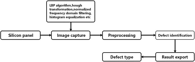
FIGURE 1. Silicon panel detection process.
Clustering [9] method completes the detection mainly by extracting the corresponding data between the area of defects and the normal background and then classifying the data according to a certain algorithm. Finally, by setting the threshold or using other segmentation algorithms, the images with only background or defects are obtained. For silicon panel defect detection, a defect detection scheme based on clustering with uniformity measures is proposed by Tsai et al. [7]. The scheme process is shown in Figure 2.
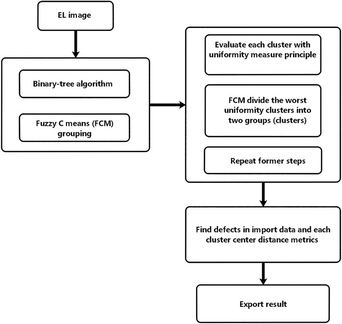
FIGURE 2. Clustering method process for silicon panel detection.
The characteristic of the clustering algorithm is that only defect-free images are used as training samples, and then a binary-tree clustering method is proposed to partition defect-free samples that involve tens of groups in the training procedure [18]. Then a uniformity measure based on principal component analysis is evaluated for each cluster as shown in Eqs 1, 2, and the current cluster with the worst uniformity of intersample distances is separated into two new clusters using the fuzzy C-means [19]. In the sample test, the distance from the collected sample data to each individual cluster center obtained by the above process is measured to determine whether the sample contains defects [20].
For j’th cluster set, the sum of square function J of the distance from each sample point in the cluster set to the center of the cluster is minimized. Sj represents the j’th cluster set, and the clustering center is Zj, and Nj represents the number of samples contained in the j’th cluster Sj [17].
The experimental results indicate that the clustering algorithm mainly focuses on the detection of linear defects and grid lines defects, including broken grids, microcracks, and grid breakage, which are also common in the producing process of solar cells. And the algorithm is not suitable for other types of defects. Moreover, the algorithm needs to determine the number of clusters C and the control constant of distance threshold [17].
Based on the analysis above, there are many detection methods for silicon panels in China and abroad, but the algorithms generally have high time complexity or incomplete functions, and some of them can not meet the needs of actual production. For the purpose of cost saving, the functions that could only be achieved by microcomputers are now done by small devices like Raspberry Pi. A new algorithm design is used for defect detection in silicon panels to achieve real-time and intuitive detection, meeting the actual needs of production. Machine vision technology can be used to help enterprises improve the accuracy of product defect detection, improve the quality of inspection, and improve the existing problems of manual quality inspection [20].
The Prewitt operator is a first-order differential operator and an average filter, which can suppress noise well. The principle of noise suppression is realized by averaging pixels, and the average process of pixels is equivalent to low-pass filtering of images [21]. The Prewitt_x edge detection operator can reflect the vertical edge of the image after convolution, and Prewitt_y convolution can reflect the horizontal edge of the image, as shown in Figure 3.
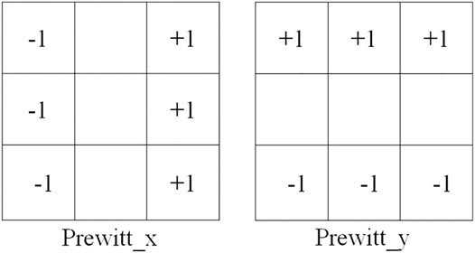
FIGURE 3. Convolution kernel of the Prewitt operator.
The Prewitt operator uses the values of nine pixels in the 3 × 3 region shown in Figure 4 to calculate the horizontal and vertical gradient values as shown in Eq. 3. By using the Prewitt operator to detect the defects of solar panels, the horizontal and vertical margin lines in solar panels can be clearly detected [22]. Through the two convolution kernels in Figure 3, it can be seen that the Prewitt_x operator is actually the nonnormalized median smoothing of the image in the vertical direction, and then the difference in the horizontal direction is calculated, while the Prewitt_y operator is actually the nonnormalized median smoothing in the horizontal direction. It is precisely for the reason of image smoothing processing that the microcrack is difficult to detect when using the Prewitt operator, but the transverse texture of the panel cell can be detected well, which lays the foundation for the subsequent elimination [23, 24].

FIGURE 4. The 3 × 3 area of an image (z represents the grayscale value).
The Canny edge detection operator represents a multilevel detection algorithm; the implementation process of this algorithm is as follows:
1) The selected image is converted to a grayscale image.
2) The image performs Gaussian filtering, and the two-dimensional Gaussian distribution matrix is generated, which can be calculated by
Then Eq. 5 is used to implement convolution filtering for grayscale image.
3) For unary function, the gradient value and direction can be calculated by derivation, and for binary function, they can be calculated by partial derivation. In image processing, the first-order finite difference of Eq. 6 is used to approximate the gradient value (change rate) of grayscale value.
where f[i, j] represents the grayscale value of the image, P[i, j] represents the gradient magnitude in the X direction, Q[i, j] represents the gradient magnitude in the Y direction, M[i, j] represents the magnitude of the point, and θ[i, j] represents the gradient direction, that is, the angle.
4) The nonmaximum suppression (NMS) is looking for the local maximum value of the pixel. Along the gradient direction, compare the gradient values at the front and back of it. If the gradient magnitude of the area is the largest in the direction of the gradient, it will be retained; otherwise, it will be suppressed.
5) The experimental results only using Prewitt operator is very sensitive to the transverse grid rather than defect characteristics at the details. So the main reason for the low accuracy lays in undetected number.
There are three criteria for Canny edge detection:
1. Low error rate edge detection: the algorithm should accurately find as many edges as possible in the image and reduce missed detection and false detection as much as possible.
2. Optimal location: the detected edge point should be accurately located at the center of the edge.
3. Any edge in the image should be marked only once, and image noise should not produce false edges.
The advantage of the Canny operator is that two different thresholds are used to detect the strong edges and the weak edges, respectively, and when they are connected, the weak edge is included in the output image.
In this article, based on the analysis of the advantages and disadvantages of solar panel detection using Prewitt and Canny operators, a solar panel defect detection algorithm combining Prewitt and Canny operators is proposed. Inheriting the advantages of Prewitt and Canny operators, the algorithm improves the accuracy of solar panel detection.
In this article, the edge extraction for all details will be better because the edge of solar panels obtained by the Canny operator is delicate, but the defect position edge obtained also contains the image edge features. Through many observations, it is found that most of the edge features in each patch of the panel extracted by the Canny operator are mainly transverse grid textures. In order to better obtain the edge characteristics of the solar panel defects, this article proposes to use Prewitt and Canny operators which are sensitive to transverse and vertical margin lines to implement image edge extract, respectively. Through the combination of the two algorithms used in this article, the defect edge characteristics of solar panels can be obtained clearly.
In this article, the specific steps of the algorithm are shown in Figure 5. The algorithm combination process is shown in Figure 5.
Step 1: The entire panel is divided by a background foreground. The background is black in the outer circle, the foreground is patches, the whole image is binarized, the threshold is set to 0; 35, and the basic contour can be roughly obtained thereby. The closing operation is used to eliminate grooves and microholes and find out the maximum communication domain, and finally a complete foreground image can be obtained.
Step 2: Locate the silicon panel patches. Since it is evenly distributed at the same size, complete small patches can be geometrically obtained.
Step 3: The image of each patch is processed separately. Since there are horizontal lines in each small block, which do not belong to defect, horizontal convolution kernel (such as the Prewitt operator) can be used to detect horizontal grid lines first. Then attention should be paid to threshold selection, and then the Canny operator can be used to detect all texture boundaries.
Step 4: Eliminate the interference of the grid lines and the boundary line around the patch and retain the defect texture. Here the grid lines detected by the Prewitt operator are inflated to obtain the mask of the nonhorizontal area and then intersect with the mask of Canny to obtain the defect location.
Step 5: Marking defect: after acquiring the identification position, then a three-channel image is reconstructed, marking the gray value of pixels at the defect location in red.
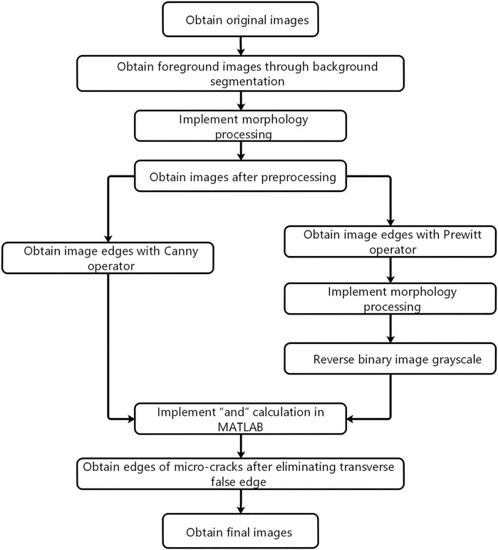
FIGURE 5. Flowchart of the algorithm proposed in the article.
The visualization of the relevant steps in the algorithm fusion process is shown in Figure 6.
1) After the original silicon panel image is preprocessed, a binary edge profile image detected by the Canny operator is obtained, as shown in Figure 6E. It can be witnessed that the defect profile in the block diagram is detected together with the edge profile of the image. The edge details are very delicate, and the image edge and the transverse grid cause a lot of false edges in the nondefective position.
2) In order to eliminate extra lines caused by the edge profile and transverse grid mentioned in (1), after preprocessing the image in procedure (1), then the edge characteristics of the solar panel are extracted by the Prewitt operator, obtaining the effect diagram as shown in Figure 6A. According to the characteristics of the Prewitt operator, it performs well when dealing with transverse and vertical edges.
3) After morphology processing, the border and the grid edge are removed as shown in Figure 6B.
4) The value of each pixel in Figure 6B is 0 or 255. The grayscale of the image is reversed by using Eq. 7 for each pixel value. In Eq. 7, r and s represent the pixel values before and after processing, L−1 represents the range of [0, L−1] of the grayscale, and the range of binary images is [0, 255]. So a binary graph is obtained as shown in Figure 6C.
5) By implementing “and” calculating each pixel point in Figures 6C,E (corresponding value 0 or 1), respectively, the transverse grid and border part of the two images can be eliminated, leaving behind the defect edge image of the silicon panel.
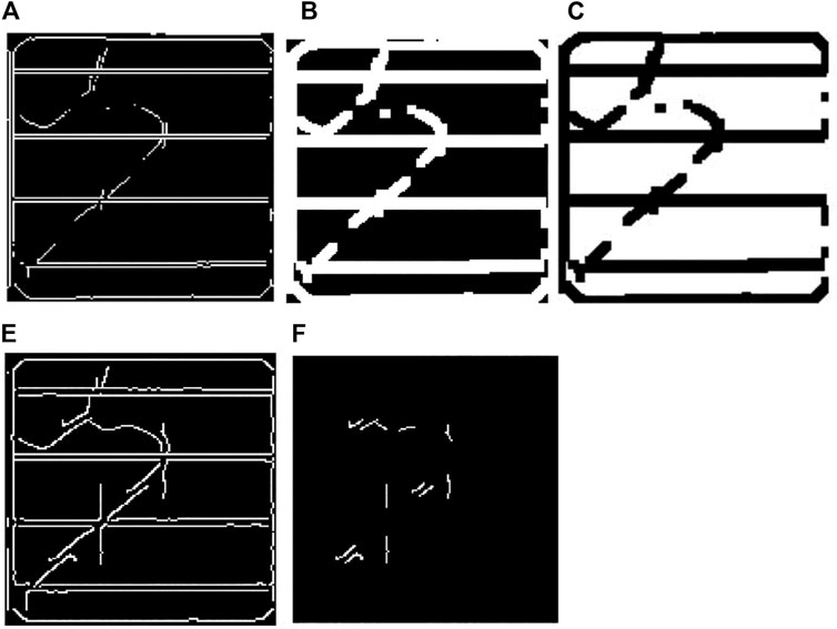
FIGURE 6. Detection effect diagram of the algorithm in this article.
In order to verify the effectiveness of the algorithm proposed in this paper, the solar panels which contain only micro-cracks are selected for comparison. And some of the defects are shown in Figure 7. Here the prewitt operator, the canny operator and algorithm in this article are used to detect whether there are defects in solar panels and find the corresponding positions of these defects.
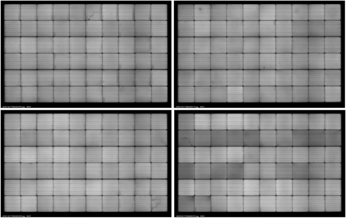
FIGURE 7. Original image of solar panel.
Through the comparison of the above three sets of detection results, it can be witnessed that there are Prewitt_x and Prewitt_y operators in the Prewitt algorithm. And the former operator is sensitive to vertical edge information which enjoys good detection, while the Prewitt_y operator is nonnormalized median smoothing of the image in the vertical direction. So it can be seen from Figure 8 that the information detected lays on more elimination of transverse false edge. When using the Prewitt operator alone and under the intervention of elimination of transverse false edge, it can be witnessed that the defect includes more edge lines during the detection procedure, which makes the false result. From the perspective of the Canny operator and combined with the result of Figure 9, the Canny operator finds out the shape of microcracks but also detects the elimination of transverse false edge. So, the detection effect of using the Prewitt operator alone and the Canny operator alone is not enough. And from Figure 10, it can be found that the microcrack position is marked in red lines and without misdetection of transverse false edges which has a great leap compared with using one single operator.
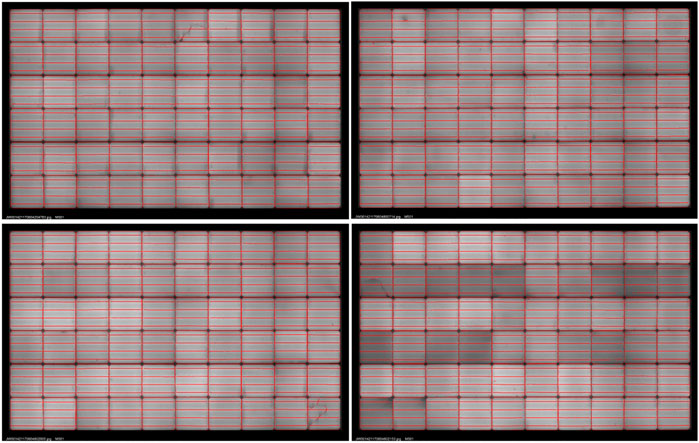
FIGURE 8. The effect diagram obtained by using the Prewitt operator alone.
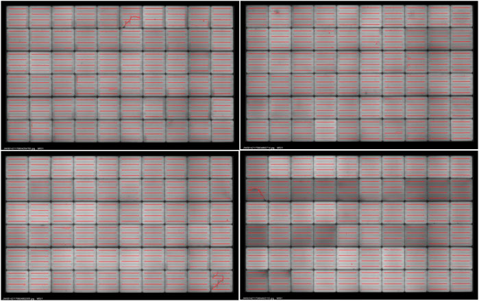
FIGURE 9. The effect diagram obtained by using the Canny operator alone.
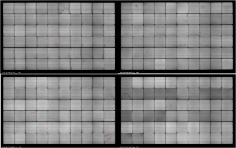
FIGURE 10. The effect of the algorithm proposed in this article.
From the analyses above, there are several different operators and each has its advantages and limitations. If the advantages of each operator can be combined, it can be ensured that the detection result will be better. Based on the idea of that, a method combined with Canny and Prewitt operators is proposed, improving the accuracy of defect detection. The combination, to a certain extent, overcomes the disadvantages of the single operator and the advantages of different operators are combined. Therefore, the method proposed in the article can detect defects in silicon panels such as microcracks effectively, and the method can get rid of the intervention of the grid edge of silicon panels.
The experimental results of the algorithm are shown in Table 1. The total number of samples is M. The number of samples with microcracks is G. The number of undetected panel is W1. The number of missed detection panel is W2. The accuracy is L1. The mistake rate is L2. And the undetected rate is L3. The relevant accuracy, mistake rate, and undetected rate are shown in Eqs 8–10.
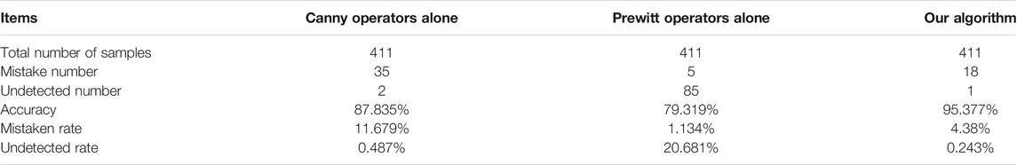
TABLE 1. Microcracks detection result.
In the table, it can be seen that the Canny operator is more delicate, but there is a problem that false edges are misdetected and undetected at the same time. According to Table 1, the reason for the low accuracy of the Canny operator is mainly due to the high mistake number. The experimental results only using Prewitt operator is very sensitive to the transverse grid, Prewitt operator is not sensitive enough when detecting irregularly shaped defects. So the main reason for the low accuracy lays in undetected number. But the algorithm proposed in this article combines the advantages of Canny and Prewitt operators, and the accuracy of the algorithm is the highest compared with the first two items.
In this experiment, the algorithm needs to preprocess the images caused by small noise, such as salt-pepper noise, but it can not smooth the features with microcracks, because this processing will reduce the sensitivity of the algorithm to the features of microcracks. So the next step is to reduce the mistake rate of the algorithm.
Focusing on silicon panel defect detection, the article proposed a detection method on the basis of the complementary advantages of Prewitt and Canny operators. This method has achieved good results in defect detection of solar panels. It has solved the problem that the mainstream convolution neural network requires a lot of training data and high hardware requirements. By using the method proposed in the article, one can intuitively detect the presence of defects in silicon panels, and it is not limited to certain fixed features of defects and the size of the anchor. Comparably speaking, the method is more generalized and robust. It can directly detect defects in silicon panels such as microcracks, improving the accuracy of detection. But as for the algorithm proposed in the article, there are limitations, especially the misdetection for the special microcracks (cracks that are completely coincidental or completely parallel with transverse grid lines). On the other hand, for the different defects of panels, the algorithm in this article cannot implement pattern recognition. Therefore, the classified recognition for various defects should be the focus of the research in the future. This method can be used by the production company for quality assurance in the silicon panel production procedure and can better detect a variety of defects in real time.
The original contributions presented in the study are included in the article/Supplementary Material; further inquiries can be directed to the corresponding author.
YZ is responsible for the overall direction of the experiment and the newly proposed points, including the writing of the paper ZW grasps the overall direction of the article, and provides more guidance for experiments and paper writing YW is responsible for the processing of related image data sets for experiments CZ is responsible for experimental records and experimental data analysis BZ is responsible for the English paper translation and article polishing.
This research was funded by the National Natural Science Foundation of China, grant number 6192007, 61462008, 61751213, 61866004; the Key projects of Guangxi Natural Science Foundation, grant number 2018GXNSFDA294001,2018GXNSFDA281009; the Natural Science Foundation of Guangxi, grant number 2018GXNSFAA294050, 2017GXNSFAA198365; 2015 Innovation Team Project of Guangxi University of Science and Technology, grant number gxkjdx201504; Research Fund of Guangxi Key Lab of Multi-source Information Mining and Security, grant number MIMS19-04; Guangxi Postgraduate Education Innovation Project, grant number GKYC202106, GKYC202104, YCSW2021320; College Students' innovation and Entrepreneurship Project 202110594133, 202110594134.
The authors declare that the research was conducted in the absence of any commercial or financial relationships that could be construed as a potential conflict of interest.
All claims expressed in this article are solely those of the authors and do not necessarily represent those of their affiliated organizations, or those of the publisher, the editors and the reviewers. Any product that may be evaluated in this article, or claim that may be made by its manufacturer, is not guaranteed or endorsed by the publisher.
1. Zhang W-j., Li D, Ye F. Texture Defect Inspection for Silicon Solar Cell. J Comput Appl (2010) 30(10):2702–4. doi:10.3724/sp.j.1087.2010.02702
2. Zhou T, Jing X. Surface-Based Detection and 6-DoF Pose Estimation of 3-D Objects in Cluttered Scenes[J]. IEEE Trans Robotics (2016) 6, 1–15.
3. Noguchi T. Fourier Transform Infrared Difference and Time-Resolved Infrared Detection of the Electron and Proton Transfer Dynamics in Photosynthetic Water Oxidation. Biochim Biophys Acta (Bba)–Bioenerg (2015) 1847(1):35–45. doi:10.1016/j.bbabio.2014.06.009
4. Nguyen TP, Debled-Rennesson I. “Circularity Measuring in Linear Time,” 2010 20th International Conference on Pattern Recognition (2010) 2098–101. doi:10.1109/ICPR.2010.1157
5. Belyaev A, Polupan O, Ostapenko S, Hess D, Kalejs JP. Resonance Ultrasonic Vibration Diagnostics of Elastic Stress in Full-Size Silicon Wafers. Semicond Sci Technol (2006) 21(3), 254–60. doi:10.1088/0268-1242/21/3/007
6. Gabor AM, Ralli M, Montminy S, Luis S, Bordanaro C, Woods J, et al. “Soldering Induced Damage to Thin Si Solar Cells and Detection of Cracked Cells in modules[C],” in 21st European Photovoltaic Solar Energy Conference, (2006) p. 2042–7.
7. Tsai D-M, Chang C-C, Chao S-M. Micro-crack Inspection in Heterogeneously Textured Solar Wafers Using Anisotropic Diffusion. Image Vis Comput (2010) 28(3):491–501. doi:10.1016/j.imavis.2009.08.001
8. Dong D, Chen G. Silicon Solar Cell Fault Detection Method Based on Near-Infrared Image[J]. J Terahertz Sci Electron Inf (2010) 08(5):539–43. doi:10.3969/j.issn.1672-2892.2010.05.009
10. Zhang H, Fu Z, Bei N, Zhang Z, Zhang R. Application of the Combination of Bimodal Method and Otsu Method in Defects Detection in Solar Cells[J]. Comput Syst Appl (2012) 21(1):115–7. doi:10.3969/j.issn.1003-3254.2012.01.027
11. Fuyuki T, Kitiyanan A. Photographic Diagnosis of Crystalline Silicon Solar Cells Utilizing Electroluminescence. Appl Phys A (2009) 96:189–96. doi:10.1007/s00339-008-4986-0
12. Demant M, Rein S, Krisch J, Schoenfelder S, Klute C, Bartsch S, et al. Detection and Analysis of Micro-cracks in Multi-Crystalline Silicon Wafers during Solar Cell Production [C]. In: 37th IEEE Photovoltaic Specialists Conference, Seattle, WA, June 19–24, 2011, (2011) 001641–6. doi:10.1109/pvsc.2011.6186271
13. Yang C, Zhang H, Huang G. The Application of Electroluminescence Imaging in the Quality Inspection of Crystalline Silicon Cells and Modules[J]. Sunshine Energy (2009)(6) 42∼43+45.
14. Liu X, Xu L, Xiao C, Cao J, Xiao J. Image Processing Technology Based on Matlab to Identify Defects in Silicon Solar Cells[J]. J Shanghai Jiaotong Univ (2010) 44(07):926–30.
15. Rösch R, Krebs FC, Tanenbaum DM, Hoppe H. Quality Control of Roll-To-Roll Processed Polymer Solar Modules by Complementary Imaging Methods. Solar Energ Mater Solar Cell (2012) 97:176–80. doi:10.19519/j.cnki.1672-3392.2020.03.014
16. Fan C. Research on High-Efficiency Detection System for Surface Defects of Solar cells[D]. Anhui University (2019).
17. Qin L. Feature Dimensionality Reduction and Clustering Methods for Photovoltaic System Fault Diagnosis Problems [D]. Hangzhou Dianzi University (2020).
18. Di Sante R, Cavaliere P, Rossi GL, Squillace A. Thermoelastic Analysis of Crack Propagation in AA6082 Friction Stir Welded Joints. Msf (2007) 561-565:2221–4. doi:10.4028/www.scientific.net/msf.561-565.2221
19. Treshansky A, Robert M. McGraw. Overview of Clustering Algorithms[J]. Proc Spie Int Soc Opt Eng (2001) 4367:41–51.
20. Tsai D-M, Li G-N, Li W-C, Chiu W-Y. Defect Detection in Multi-crystal Solar Cells Using Clustering with Uniformity Measures. Adv Eng Inform (2015) 29(3):419–30. doi:10.1016/j.aei.2015.01.014
21. Li M. Color Classification and Defect Detection of Solar Panels Based on Machine Learning [D]. Hebei University of Technology (2019).
22. Cui D. Research on Crack Detection Algorithm for Polycrystalline Solar Cells [D]. Dalian Maritime University (2019).
23. Zhang Y, Cheng X, Cui H, Cheng S, Zhang X, Zhang F. Recognition of Hole Defects in Composite Radiographic Images Based on Convolutional Neural Network[J]. Optics Optoelectron. Technol (2020) 18(03):75–80.
24. Huan C. On-line Detection Method for Woven Bag Defects Based on Machine vision[J/OL]. Prog Laser Optoelectronics 1-13. Available at: http://kns.cnki.net/kcms/detail/ 31.1690.TN.20200610.1454.060.html. (Accessed 2020-06-15).
Keywords: silicon panel, edge detection, defect detection, prewitt operator, canny operator
Citation: Zhang Y, Wang Z, Wang Y, Zhang C and Zhao B (2021) Research on Image Defect Detection of Silicon Panel Based on Prewitt and Canny Operator. Front. Phys. 9:701462. doi: 10.3389/fphy.2021.701462
Received: 07 May 2021; Accepted: 09 July 2021;
Published: 16 August 2021.
Edited by:
Olivier J. F. Martin, École Polytechnique Fédérale de Lausanne, SwitzerlandReviewed by:
Mohammad Abu Yousuf, Jahangirnagar University, BangladeshCopyright © 2021 Zhang, Wang, Wang, Zhang and Zhao. This is an open-access article distributed under the terms of the Creative Commons Attribution License (CC BY). The use, distribution or reproduction in other forums is permitted, provided the original author(s) and the copyright owner(s) are credited and that the original publication in this journal is cited, in accordance with accepted academic practice. No use, distribution or reproduction is permitted which does not comply with these terms.
*Correspondence: Zhiwen Wang, d3p3NjlAMTI2LmNvbQ==
Disclaimer: All claims expressed in this article are solely those of the authors and do not necessarily represent those of their affiliated organizations, or those of the publisher, the editors and the reviewers. Any product that may be evaluated in this article or claim that may be made by its manufacturer is not guaranteed or endorsed by the publisher.
Research integrity at Frontiers
Learn more about the work of our research integrity team to safeguard the quality of each article we publish.