 Yingzhi Zhao
 Lingyun Xie1
 Xingyu Wang
 Guofu Zhou
94% of researchers rate our articles as excellent or good
Learn more about the work of our research integrity team to safeguard the quality of each article we publish.
Find out more
ORIGINAL RESEARCH article
Front. Phys., 04 May 2021
Sec. Optics and Photonics
Volume 9 - 2021 | https://doi.org/10.3389/fphy.2021.684283
This article is part of the Research TopicPhysical Model and Applications of High-Efficiency Electro-Optical Conversion DevicesView all 24 articles
The heterostructuring and doping concepts have proved to obtain a novel n-InGaN/p-Cu2O nanowire (NW) photoanode by strong enhancement of the photocurrent compared to a bare InGaN NW photoanode in solar water splitting. The large photocurrent is due to the maximized photocarrier separation and hole transfer to the surface in the depletion zone of the p–n heterojunction established by the p-Cu2O layer, forming a thin, uniform shell-layer around the n-InGaN NW core by electrodeposition. For sufficiently thin Cu2O layers, the upward energy band bending in the depletion zone extends up to the surface for optimized hole transport and surface reaction. Thick Cu2O layers on top of the InGaN NWs act as common photocathodes. The functional InGaN/Cu2O heterostructure core-shell NW photoanode is chemically self-stabilized at positive applied voltage by a thin CuO surface layer. Final deposition of the earth-abundant NiOOH co-catalyst boosts the photocurrent of the InGaN/Cu2O/NiOOH complete NW photoanode into the competitive mA/cm2 range.
The key strategies to boost the performance of photoelectrodes are nanostructuring, surface catalyst coupling, light management, heterostructuring, and doping to optimize the crucial processes of light absorption, photocarrier separation and transfer, and surface reaction [1, 2]. To begin with the right material, InGaN is one of the best choices due to the wide tunability of the direct optical bandgap over the whole visible range by varying the In content, the high absorption coefficient, high carrier mobility, and chemical and mechanical resilience [3–5]. In addition, for one of the most important reactions, the photoelectrochemical splitting of water into hydrogen and oxygen [6–8], InGaN possesses the required straddling alignment of the conduction band and valence band with the water H+/H2 reduction potential and O2/H2O oxidation potential for up to ~50% of the In content and shows the best bandgap energy for solar light absorption for 30–40% In [9]. Solar hydrogen produced by this method of photoelectrochemical water splitting is the ideal green fuel to replace fossil fuels in a sustainable hydrogen energy economy1.
Nanostructured n-type InGaN nanowires (NWs) and InGaN layers, activated with InN quantum dots (QDs), employed as photoanodes, showed high efficiencies in the oxygen evolution reaction (OER) in solar water splitting [10–16]. The underlying difference between these two approaches is the type of surface states for the m-plane InGaN NW sidewalls and the c-plane surface of the InGaN layers and InN QDs. m-Planes exhibit negatively charged surface states within the energy bandgap, causing near-surface upward energy band bending, which is most commonly encountered in the n-type semiconductors. The c-plane of In-rich InGaN layers exhibits positively charged surface states located within the conduction band [17–21]. These positively charged surface states catalyze the OER by attraction of electrons, which is strongly enhanced by the zero-dimensional electronic properties of InN QDs. For m-planes, in contrast, a low catalytic activity for the OER results from the negatively charged surface states. Therefore, to benefit from the largely increased surface area of NWs, additional measures need to be taken to obtain competitive water splitting efficiencies, such as the decoration of the NW sidewalls with co-catalysts. InGaN NWs have also demonstrated their successful light management and absorption enhancement, acting as efficient anti-reflection structures when grown on pyramid-patterned Si substrates [22].
In this study, we demonstrate the heterostructuring and doping routes for an InGaN/Cu2O core-shell NW photoanode to boost solar water splitting by enhancing the separation and transport of photogenerated carriers. The underlying concept is as follows: A heterostructure with the right staggered band alignment, such that no energy barriers for the transport of electrons and holes are present, can improve the photogenerated carrier separation and transport. However, it is only effective together with the right band bending given by the doping. Based on an n-type photoanode with near-surface upward energy band bending, a p-type layer on top is optimum to increase the upward energy band bending at the p–n junction. Together with a positive band offset, this pushes the holes toward the surface more effectively for the OER and also enhances the electrons to travel toward the cathode for the hydrogen evolution reaction (HER). A p-type layer, however, exhibits the wrong near-surface downward energy band bending, opposing the hole transport toward the surface. Therefore, the p-type layer has to be sufficiently thin, such that it is fully depleted and the upward energy band bending proceeds all the way to the surface. This turns a p-type layer, usually acting as photocathode into an active surface layer, by boosting the efficiency of an n-type photoanode. For the optimized bandgap energy for solar light absorption of the n-type photoanode, the p-type layer on top ideally has a similar, medium bandgap energy to contribute to the absorption. Regarding the OER, however, the surface of the p-type layer is not necessarily reactive, still requiring the deposition of co-catalysts.
Considering the band alignment, doping, and bandgap energy, p-type Cu2O fulfills all the requirements when combined with n-type In-rich InGaN as a heterostructure photoanode. Photogenerated carrier separation and transfer are strongly enhanced in the depletion zone of the p–n heterojunction formed at the n-InGaN/p-Cu2O heterointerface with positive band offset. This is based on a previous study where we showed that Cu2O, a deeply studied p-type metal-oxide, acts as an efficient hole injection and a collection layer on In-rich InGaN NWs, solving the p-type conductivity problem [23]. High-quality p-type InGaN with a high In content is hardly realized. The bandgap energy of Cu2O of 2.1 eV is sufficiently small and the conduction band and valence band of Cu2O are well-aligned with those of the In-rich InGaN with the right band offsets.
Cu2O is electrodeposited on the InGaN NWs. Scanning electron microscopy (SEM), transmission electron microscopy (TEM), and energy dispersive X-ray spectroscopy (EDS) reveal that Cu2O forms a uniform shell-layer on the m-plane InGaN NW sidewalls while nucleating as isolated Cu2O nanocrystals on the c-plane NW tops. p-Type Cu2O is well-known as a photocathode for the HER [24, 25]. This is reproduced for thick Cu2O layers grown on top of the InGaN NWs. Similar to InGaN, Cu2O also exhibits a straddling energy band alignment with the water redox potentials [25–28], making the energy band alignment with InGaN most obvious. For thin Cu2O layer deposition, the Cu2O shell-layers on the InGaN NWs are fully depleted for thicknesses of ~10 nm with upward energy band bending up to the surface. The efficient photocarrier separation and hole transport to the surface strongly enhance the OER reaction for positive applied voltage, as shown by linear sweep voltammetry (LSV) measurements and current density vs. time (I–t) measurements under chopped illumination. For optimized Cu2O deposition amount, an almost 7-fold enhancement of the photocurrent is observed. Electrochemical impedance spectroscopy (EIS), however, shows that the Cu2O surface is catalytically not very active for the OER, such as the m-plane InGaN NW sidewalls, leading to an overall insufficient photocurrent. Therefore, to achieve competitive photocurrents, NiOOH co-catalyst is electrodeposited to complete the photoanode preparation process. NiOOH is chosen because it contains only earth-abundant elements. Functioning as InGaN/Cu2O core-shell NW photoanode at positive applied voltage, the Cu2O layer is chemically self-stabilized by the formation of a thin CuO surface layer due to the self-limiting oxidation of Cu2O, as evidenced by the LSV measurements, cyclic voltammetry (CV) measurements, and X-ray photoelectron spectroscopy (XPS). Although imposing a small energy barrier for the hole transport, the thin CuO surface layer does not significantly influence the photocurrent. In contrast to Cu2O employed as photocathode at negative applied voltage, no other surface passivation is needed. The InGaN/Cu2O heterostructure core-shell NW photoanode, self-passivated with the thin CuO surface layer, shows no degradation for many hours of operation.
The InGaN NWs on planar p-type Si (111) substrates were fabricated by plasma-assisted molecular beam epitaxy (PA-MBE). The In and Ga metal fluxes were provided by standard Knudson effusion cells, and the active nitrogen species were generated with a radio frequency (RF) plasma source. Before loading into the MBE chamber, the Si substrates were etched in 10 wt% HF aqueous solution for 1 min to remove the native surface oxide layer. Then, the cleaned Si substrates were loaded into the MBE buffer chamber and degassed in the MBE middle chamber for 1 h at 300°C. The Si substrates were then transferred to the MBE growth chamber, outgassed for 10 min at 900°C (thermocouple reading) to remove any residual native surface oxide, and exposed to active N flux for 5 min to form a thin SiNx layer. The RF power for the Si surface nitridation was 350 W, and the molecular N2 flow rate was 1.7 standard cubic centimeters per minute (sccm). The SiNx layer improves the InGaN crystal quality by enhancing strain relaxation and reducing the dislocation density. For not too extended nitridation, the SiNx interlayer does not alter the electronic properties/near-ohmic behavior of the Si/InGaN interface [29]. For InGaN growth, the substrate temperature was ramped down to 610°C (thermocouple reading) and InGaN growth under N-rich conditions was performed by opening the In and Ga cell shutters for 1 h. The In and Ga beam equivalent pressure was 7.60 × 10⁻⁸ and 1.32 × 10⁻⁷ Torr, respectively, and the active N source parameters were 350 W and 1.7 sccm molecular N2 flux.
The samples were coated with In–Ga eutectic on the back side of the substrate to form an ohmic contact, glued on Cu-conductive adhesive tape, and fixed on a supporting glass plate. The surface was covered with non-transparent silicone rubber, leaving an opening for contact with the electrolyte.
The Cu2O layers were fabricated on the InGaN NWs by electrodeposition in a three-electrode electrochemical cell using an electrochemical work station. The InGaN NWs, a Pt mesh, and a saturated calomel electrode (SCE) were used as working, counter, and reference electrodes, respectively. The aqueous electrolyte comprised 0.4 M CuSO4, 3 M lactic acid, and C3H6O3. The pH was adjusted to 12 by adding 5 M NaOH. The deposition voltage was kept at −0.4 V vs. SCE. During deposition with magnetic stirring at 180 rpm, the temperature was set to 27°C by a hot plate with a temperature sensor in the solution.
The InGaN/Cu2O/NiOOH structures were prepared by electrodeposition in a three-electrode electrochemical cell with the InGaN/Cu2O working electrode, a Pt mesh counter electrode, and a saturated KCl Ag/AgCl reference electrode, connected to an electrochemical workstation. The electrolyte was 100 mL of 5 mM Ni(NO3)2·6H2O aqueous solution. The potential was kept at −1.0 V vs. Ag/AgCl. The optimized electrodeposition time was 330 s.
Structural analysis of the InGaN NWs and Cu2O layer was performed using X-ray diffraction (XRD) (PANalytical X'Pert PRO). Field-emission SEM (ZEISS Gemini 500), TEM (JEM-2100HR), and atomic force microscopy (AFM, Bruker MultiMode 8) were used to characterize the surface morphology and cross-section of the structures. EDS element mappings were carried out with energy disperse spectrometers (Aztec X-Max 80) attached to the SEM and TEM. XPS was conducted with XPS spectrometers (EscaLab 250Xi) attached to the SEM and TEM. The XPS spectra were calibrated with respect to the C 1s peak. Raman spectroscopy was performed with the 532 nm line of a Nd-YAG solid-state laser. The diameter of the laser spot was ~1 μm. Photoluminescence (PL) spectra were taken at room temperature with the 100 mW, 532 nm line of a Nd-YAG solid-state laser as excitation source, and a silicon charged coupled device (CCD) attached to a single monochromator for detection.
The electrochemical measurements were performed in a three-electrode electrochemical cell with the InGaN, InGaN/Cu2O, and InGaN/Cu2O/NiOOH working electrodes; a Pt mesh counter electrode; and a saturated KCl Ag/AgCl reference electrode connected to an electrochemical workstation. A scheme of the experimental setup and sample structure is shown in Supplementary Figure 1. The electrolyte was 0.5 M Na2SO4 (pH = 7) aqueous solution. LSV current vs. voltage (I–V) measurements from +1 V to 0 V vs. Ag/AgCl [+1.6 V to +0.6 V vs. the reversible hydrogen electrode (RHE)] with 10 mV s−1 scan rate and I-t measurements at 0.6 V vs. Ag/AgCl (1.2 V vs. RHE) were performed under chopped 5 s on and 5 s off simulated sun light (1-sun, AM 1.5, 100 mW cm−2, GLORIA-X500A). EIS measurements were conducted in the frequency range of 10 Hz to 1,000 kHz in the dark and light. CV measurements were performed in the voltage windows of −1 V to +1 V and 0 V to +1 V vs. Ag/AgCl with a 100 mV s−1 scan rate.
Figures 1a,b shows the SEM top-view and cross-sectional images of the as-grown, bare InGaN NWs on a Si (111) substrate. The NWs have an average diameter of 40 nm, 600 nm length, and a flat top. After 40 s of Cu2O electrodeposition, which turns out to be the optimum Cu2O electrodeposition time, sparse, isolated Cu2O nanocrystals are visible in the top-view SEM image in Figure 1b. AFM images are shown in Supplementary Figure 2. The nanocrystals are positioned on the NWs and also in-between NWs with arbitrary orientations. The shape of the nanocrystals reflects the cubic crystal symmetry of Cu2O. The more connected appearance of the NWs in the cross-sectional image in Figure 1c indicates the deposition of Cu2O on the InGaN NW sidewalls. Formation of the pure Cu2O phase for the present electrodeposition condition is confirmed by the omega-two-theta XRD spectrum shown in Supplementary Figure 3A and by the Raman spectrum in Supplementary Figure 3B [23]. Only peaks from cubic Cu2O, InGaN, and Si, as labeled, are observed. From the XRD spectrum, the In content of the InGaN NWs of 28% is deduced [30]. However, XPS measurements (Figure 1e) that were taken some days after fabrication of the Cu2O layer revealed the presence of CuO. As XRD and Raman spectroscopy rather probe the bulk material, XPS is highly surface sensitive, indicating the self-limiting oxidation of Cu2O to CuO in air to form a thin surface layer of CuO [31]. This is further discussed in the section Stability on the stability of the InGaN/Cu2O heterostructure operated as photoanode.
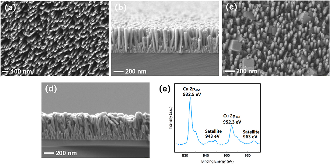
Figure 1. Top-view- and cross-sectional SEM images of the (a,b) bare InGaN nanowires (NWs) and (c,d) InGaN NWs after 40 s Cu2O electrodeposition. (e) X-ray photoelectron spectroscopy taken several days after Cu2O electrodeposition.
The element distributions are imaged by EDS mappings shown in Figure 2. The mappings are taken from the NW cross-sectional part shown in the SEM image in Figure 2a. Figure 2b displays the total EDS intensity. The individual mappings of In, Ga, N, Cu, O, and Si are shown in Figures 2c–h, respectively. The mappings of In, Ga, N, and Si show the uniform element distribution in the InGaN NWs on the Si substrate. The Cu and O element distributions reveal the deposition of Cu2O on the NW sidewalls, penetrating from the top to the bottom with decreasing EDS intensities.
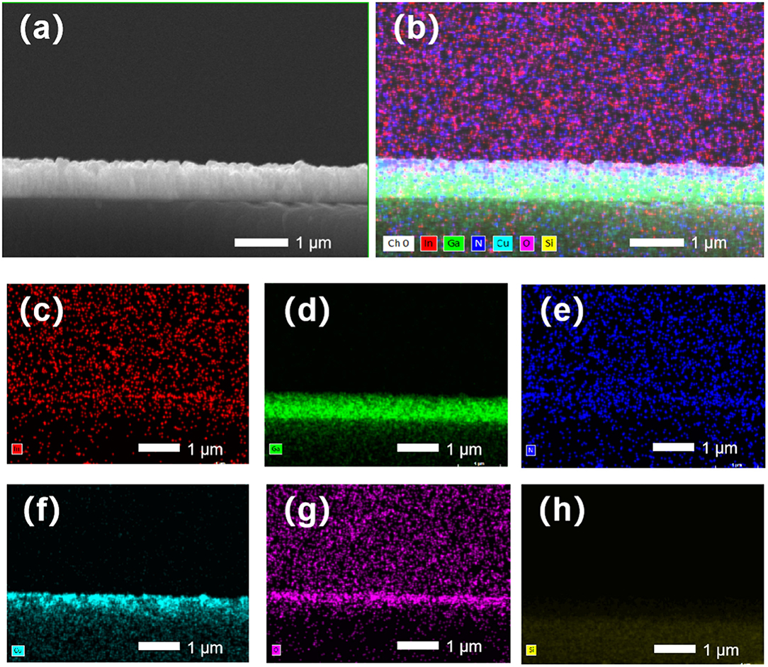
Figure 2. (a) Cross-sectional SEM image and (b–h) energy dispersive X-ray spectroscopy (EDS) element mappings. (b) Total EDS intensity and (c–h) In, Ga, N, Cu, O, and Si element mappings.
The deposition of Cu2O on the InGaN NW sidewalls is directly resolved in the TEM image in Figure 3a, and the corresponding EDS element mappings of In, Ga, N, and Cu are shown in Figures 3b–f. Figure 3b gives the total EDS intensity and Figures 3c–f depict the individual In, Ga, N, and Cu element mappings. The element contrast for O, which is not shown, is very weak. Cu2O forms a rather uniform shell on the InGaN NW sidewalls. The Cu2O shell is composed of ultra-small nanocrystals, of ~5 nm in diameter, with random orientation, seen in the high-resolution TEM image in the inset of Figure 3a. The spaces between the NWs are not completely filled. The element distributions of In, Ga, and N follow the straight geometry of the InGaN NWs. The element distribution of Cu is more blurred and smeared out, as expected for the InGaN/Cu2O core-shell structure. The different Cu2O electrodeposition behavior on the InGaN NW sidewalls and NW tops is addressed in the following section.
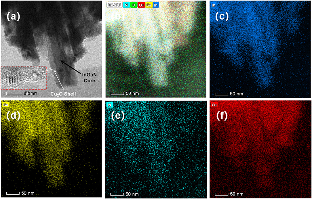
Figure 3. (a) Cross-sectional TEM image and (b–f) EDS element mappings. (b) Total EDS intensity and (c–f) In, Ga, N, and Cu element mappings. The inset in (a) is a high-resolution TEM image of the Cu2O shell-layer.
Figure 4A depicts the LSV curves for the InGaN/Cu2O core-shell NWs and for the bare InGaN NWs under chopped 1-sun (AM 1.5, 100 mW/cm2) illumination. The Cu2O electrodeposition time is 40 s. The LSV scan is taken from +1 V to 0 V vs. Ag/AgCl (1.6 V to 0.6 V vs. RHE) with a scan rate of 10 mV/s. In the presence of the Cu2O shell, the photocurrent density at positive voltage is enhanced by up to 700%. At negative voltage, no photoresponse is observed, as seen in the CV scan from +1 V to −1 V in Supplementary Figure 4A. This demonstrates the role of Cu2O in enhancing the OER when the InGaN/Cu2O core-shell NWs operate as photoanodes. The optimum Cu2O electrodeposition time of 40 s is provided from the plot of the photocurrent density vs. electrodeposition time, which is taken for an applied voltage of +0.6 V vs. Ag/AgCl (1.2 V vs. RHE), as shown in Figure 4B. When the Cu2O deposition time is increased much longer, the individual cubic Cu2O nanocrystals on top of the InGaN NWs, as shown in the SEM image in Figure 1c, increase in density and coalesce to form a compact layer. For such thick Cu2O layers, the usual behavior of Cu2O as a photocathode for the HER at negative voltage is recovered, as shown in the LSV and I–t curves in Supplementary Figures 4B–D. In this case, there is no photoresponse for positive voltage. This confirms that the thin Cu2O shell-layer is responsible for the enhanced photoanode performance, whereas the much thicker/larger cubic Cu2O nanocrystals act as photocathodes.
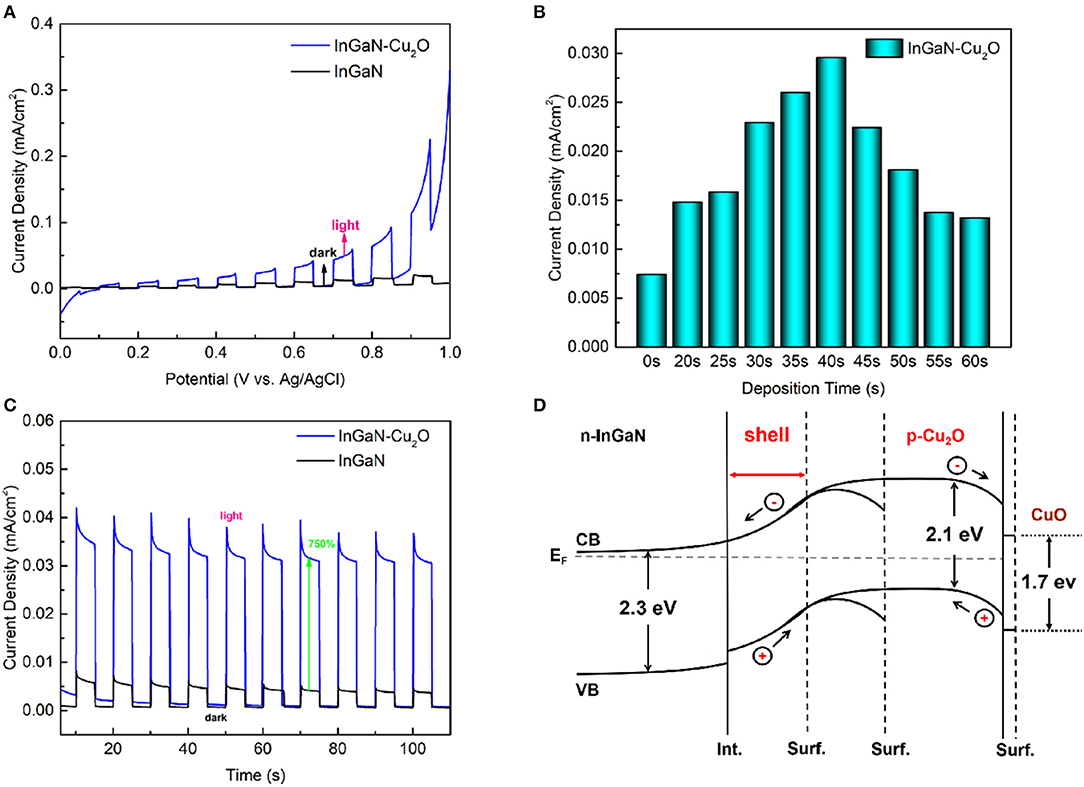
Figure 4. (A) Linear sweep voltammetry measurements of the InGaN/Cu2O core-shell NWs and the bare InGaN NWs under chopped illumination. (B) Photocurrent density at +0.6 V vs. Ag/AgCl (1.2 V vs. reversible hydrogen electrode [RHE]) as a function of the Cu2O electrodeposition time. (C) I–t measurements at +0.6 V vs. Ag/AgCl (1.2 V vs. RHE) of the InGaN/Cu2O core-shell NWs and the bare InGaN NWs under chopped illumination. (D) Scheme of the InGaN/Cu2O energy band diagram and photogenerated carrier transport for increasing Cu2O layer thickness. Int. indicates the InGaN/Cu2O interface and Surf. indicates the surface of Cu2O shell-layers with different thicknesses. The thin CuO surface layer is also shown.
A first indication of the reproducibility and stability of the InGaN/Cu2O core-shell NW photoanode is given by the I–t curve taken at +0.6 V vs. Ag/AgCl (1.2 V vs. RHE) under chopped 1-sun illumination in Figure 4C with the curve for the bare InGaN NWs for comparison. The curves reproduce a 700% increase of the photocurrent density in the presence of the Cu2O shell-layer, in agreement with the LSV measurements, and a good photo-switching behavior is observed.
The increased photocurrent density is attributed to the p–n junction with related upward energy band bending, formed at the InGaN/Cu2O interface for the m-plane NW sidewalls. The upward energy band bending enhances the separation of the photogenerated carriers and the transport of photogenerated holes toward the surface. This is maximized for sufficiently thin and fully depleted Cu2O layers on the NW sidewalls when the upward energy band bending continues to the surface. This is guaranteed for up to a Cu2O thickness where the energy band positions at the surface, taking into account only the ionized acceptor density, reach the values given by the downward energy band bending for bulk Cu2O of typically 0.4 V, which are, in turn, given by the surface Fermi-level pinning. This accounts for the increase of the photocurrent at positive voltage with increasing Cu2O shell-layer thickness, passing up to a maximum and finally reverse with photoresponse at negative voltage for thick Cu2O layers on the InGaN NW tops. The sparse cubic Cu2O nanocrystals formed together with the Cu2O shell-layers do not affect the photoanode behavior. Their size rather indicates near-surface downward energy band bending without photoresponse for positive voltage. A scheme of the described InGaN/Cu2O energy band structure and photogenerated carrier transport for increasing Cu2O shell-layer thickness is drawn in Figure 4D. The thin CuO surface layer [32] formed due to the self-limiting oxidation of Cu2O, which is discussed in more detail below, is also indicated.
The maximum photocurrent density for a Cu2O shell-layer thickness of several 10 nm agrees with typical ionized acceptor densities for Cu2O of 1015–1016 cm−3 and the related width of the depletion zone [33, 34]. However, the decrease of the photocurrent density might set in before the maximum width of the Cu2O depletion zone is utilized because of filling up of the spaces between the InGaN NWs with Cu2O, whereas the light absorption in the Cu2O layer might contribute to the increase of the photocurrent density with Cu2O layer thickness. Unfortunately, we have no direct experimental access to the electrical properties of the thin Cu2O shell-layers electrodeposited on the InGaN NW sidewalls.
Apart from that, in contrast to the rectifying p–n junction for Cu2O on the m-plane InGaN NW sidewalls, leading to the upward energy band bending, the electrical contact is more ohmic for Cu2O on the c-plane NW tops [23], not supporting the upward energy band bending. This has been attributed to the varying characteristics of the surface states for the m-plane and the c-plane of In-rich InGaN: Negatively charged surface states in the bandgap for the m-plane vs. positively charged surface states in the conduction band for the c-plane of In-rich InGaN, leading to upward/downward near-surface energy band bending for the m-plane/c-plane for In-rich InGaN and, accordingly, to near-surface electron depletion for the m-plane/near-surface electron accumulation for the c-plane of In-rich InGaN.
The different characteristics of the surface states and resulting InGaN/Cu2O electrical contact for the m-plane and the c-plane of In-rich InGaN may also explain the different electrodeposition behavior of Cu2O on the m-plane NW sidewalls and c-plane NW tops. The formation of the rectifying p–n junction for Cu2O electrodeposition on the NW sidewalls, which is forward biased under the electrodeposition conditions, might lead to a more controlled, charge-transfer limited, quasi-two-dimensional growth with the nucleation and fast coalescence of ultra-small and dense Cu2O nanocrystals. The more ohmic resistance for the NW tops might favor mass-transport limited growth, leading to the larger, randomly oriented three-dimensional Cu2O nanocrystals with lower density, as usually observed on conductive substrates [35].
The PL spectra taken at room temperature from the InGaN/Cu2O core-shell NWs and the bare InGaN NWs are shown in Figure 5A. The PL intensity for the InGaN/Cu2O core-shell NWs is significantly reduced. This is the PL from InGaN. No PL is observed from Cu2O. The PL process is fairly complex, involving light absorption, photogenerated carrier relaxation and diffusion, and radiative electron–hole recombination. However, the reduced PL intensity for InGaN and the absence of PL from Cu2O strongly support the enhanced photogenerated carrier separation and transfer in the presence of the Cu2O shell-layer. The radiative electron–hole recombination is suppressed, overcompensating the absorption, which might be enhanced by the Cu2O shell-layer.
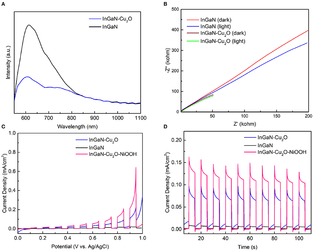
Figure 5. (A) Photoluminescence (PL) spectra taken at room temperature of the InGaN/Cu2O core-shell NWs and the bare InGaN NWs. (B) Electrochemical impedance spectroscopy (EIS) taken at +0.6 V vs. Ag/AgCl (1.2 V vs. RHE) in the dark and under illumination of the InGaN/Cu2O core-shell NWs and the bare InGaN NWs. (C) LSV- and (D) I–t measurements at +0.8 V vs. Ag/AgCl (1.4 V vs. RHE) of the InGaN/Cu2O/NiOOH complete NW photoanode and the InGaN/Cu2O core-shell NWs under chopped illumination.
With regard to all the steps in photoanode operation, i.e., absorption, photocarrier separation and transfer, and surface reaction, however, the Cu2O surface is not anticipated to exhibit particular surface catalytic activity for the OER reaction. This is seen in the EIS measurements shown in Figure 5B of the InGaN/Cu2O core-shell NWs and the bare InGaN NWs taken at an applied voltage of +0.6 V in the dark and under illumination. The half-circle in the Nyquist plots, whose diameter gives the charge transfer resistance, Rct, is large for the InGaN/Cu2O core-shell NWs and for the bare InGaN NWs, indicating an overall large Rct. To be precise, Rct includes the charge transfer through the surface in the dark plus the charge transfer toward the surface inside the photoanode under illumination. Therefore, the large Rct for the InGaN/Cu2O core-shell NWs, which is also under illumination, indicates a dominating slow charge transfer through the surface, resulting in a slow surface reaction. Therefore, to demonstrate competitive photocurrent densities, the photoanode fabrication process is completed by the electrodeposition of NiOOH co-catalyst comprising only earth-abundant elements. As shown in Figures 5C,D, the LSV and I–t curves (at +0.8 V, where the dark current continues to be low) of the InGaN/Cu2O/NiOOH complete NW photoanode and the InGaN/Cu2O core-shell NW photoanode demonstrate that photocurrent densities, reaching the mA/cm2 regime, are achieved.
Figure 6 shows the CV curves recorded from −1 V to +1 V vs. Ag/AgCl and back in the dark and under 1-sun illumination with a scan rate of 100 mV/s for the bare InGaN NWs in Figure 6A, the InGaN/Cu2O core-shell NWs in Figure 6B, and the InGaN/Cu2O/NiOOH complete NW photoanode in Figure 6C. The bare InGaN NWs show solely capacitative behavior without reaction peaks, whereas the InGaN/Cu2O core-shell NWs exhibit distinct reduction and oxidation peaks at −0.46 V and +0.3 V, respectively. These are again absent for the InGaN/Cu2O/NiOOH complete NW photoanode. This indicates excellent chemical stability of the bare InGaN NWs, which has been widely reported in previous studies, whereas the InGaN/Cu2O core-shell NWs exhibit reduction and oxidation reactions. This is well-known and has been deeply investigated for the reduction and oxidation of thick Cu2O layers used as photocathodes [25]. The NiOOH co-catalyst stabilizes the Cu2O shell-layer by promoting the water splitting rather than the reduction and oxidation of Cu2O.
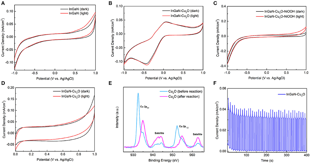
Figure 6. Cyclic voltammetry (CV) curves taken in the dark and under illumination of the (A) bare InGaN NWs, (B) InGaN/Cu2O core-shell NWs, (C) InGaN/Cu2O/NiOOH complete photoanode, and (D) InGaN/Cu2O core-shell NWs. (E) XPS spectra taken from the InGaN/Cu2O core-shell NWs before and after the water splitting experiment. (F) I–t measurement at +0.6 V vs. Ag/AgCl (1.2 V vs. RHE) for the InGaN/Cu2O core-shell NWs under chopped illumination.
Importantly, as we show in this study, the InGaN/Cu2O core-shell NWs without NiOOH are stable when operated solely at positive voltage as photoanode. They are self-stabilized by a thin CuO surface layer. The chain of arguments goes as follows: (i) The oxidation peak at positive voltage occurs only after prior scanning over the reduction peak at negative voltage, as is done for the CV measurements (Figure 6B). When scanning only from 0 V to +1 V and back, while avoiding the reduction peak, no reaction peaks are visible in the CV curves (Figure 6D). Also, when scanning from +1 V to 0 V or to −1 V, no oxidation peaks were visible in the LSV measurements in Figure 4A and Supplementary Figure 4A. (ii) XPS shows that the oxidation peak originates from the oxidation of Cu2O to CuO. In the XPS taken after scanning at positive voltages, as shown in Figure 6E, the CuO-related features are enhanced compared to those in the XPS taken before, as shown in Figure 1e. We do not exclude that the oxidation of Cu contributes to the oxidation peak after prior reduction of Cu2O [36]. However, this is irrelevant for the photoanode operation as no Cu-related features are observed in the XPS after scanning at positive voltage. (iii) In the I–t measurement taken over an extended duration of time at +0.6 V under chopped illumination, as shown in Figure 6F, an initial dark current is observed. This dark current appears when the measurement is started after prior to reduction at negative voltage. The dark current vanishes within 100 s. The photocurrent appears unaffected over the whole measurement. The total current and the dark current initially decrease with the same rate and finally, the total current equals the photocurrent and becomes very stable. Altogether, from observations (i)–(iii), there is oxidation of Cu2O in air and at positive voltage, forming a thin surface layer of CuO, as already discussed in the context of the XRD, Raman, and XPS measurements. The oxidation quickly saturates such that the Cu2O layer becomes self-stabilized by the thin CuO surface layer. Photo-oxidation is not involved in CuO formation as only the dark current changes but the photocurrent does not. The formation of a nanoscale thin, self-limiting surface oxide is all-too-common for materials which can undergo oxidation, such as those observed for the bare InGaN photoanode and Si. The self-limiting thickness is expected, considering that Cu2O is the most stable Cu oxide. In TEM, the presence of the CuO layer is not seen. Importantly, the thin CuO surface layer does not significantly affect the photocurrent, although it imposes a small energy barrier for hole transport, as indicated in Figure 4D. Hole transport might be easy because of thermionic emission and tunneling or because the thin CuO layer is leaky for the transition of holes. Self-stabilized by the thin CuO surface layer, Supplementary Figure 5 shows that the InGaN/Cu2O photoanode only exhibits a very small photocurrent decrease after many hours of operation.
Large enhancement of the photocurrent is achieved for a novel n-InGaN/p-Cu2O NW photoanode compared to a bare InGaN NW photoanode for the OER in solar water splitting. The electrodeposited Cu2O layer forms a thin shell around the InGaN NW cores. The enhancement of the photocurrent is due to maximized photogenerated carrier separation and hole transfer to the surface in the fully depleted Cu2O shell-layer of the p–n Cu2O/InGaN heterojunction. Thick Cu2O layers on top of the InGaN NWs act as usual photocathodes for the HER. The functional InGaN/Cu2O heterostructure core-shell NW photoanode is chemically self-stabilized at positive applied voltage by a thin CuO surface layer. The photocurrent reaches the competitive mA/cm2 range after final deposition of the earth-abundant NiOOH co-catalyst, establishing the InGaN/Cu2O/NiOOH complete NW photoanode. Moreover, this is an important proof of the successful formation of a rectifying p–n junction at the InGaN/Cu2O heterointerface with the Cu2O layer acting as an efficient hole collection and transport layer on In-rich InGaN, solving the p-type doping problem with far-reaching impact for devices.
The original contributions presented in the study are included in the article/Supplementary Material, further inquiries can be directed to the corresponding author/s.
YZ performed the growth and the measurements with the support of LX. GZ and RN discussed and interpreted the results. RN supervised the research and drafted the manuscript together with YZ. All authors discussed and commented on the manuscript and read and agreed to the published version of the manuscript.
This study was supported by: the Program for Chang Jiang Scholars and Innovative Research Teams in Universities (No. IRT_17R40), the Science and Technology Program of Guangzhou (No. 2019050001), the Guangdong Provincial Key Laboratory of Optical Information Materials and Technology (Grant No. 2017B030301007), the Provincial Natural Science Foundation of Guangdong program (Grant No. 2018A030313368), the MOE International Laboratory for Optical Information Technologies, and the 111 Project.
The authors declare that the research was conducted in the absence of any commercial or financial relationships that could be construed as a potential conflict of interest.
The Supplementary Material for this article can be found online at: https://www.frontiersin.org/articles/10.3389/fphy.2021.684283/full#supplementary-material
1. ^Hydrogen program. Available online at: https://www.hydrogen.energy.gov.
1. Jian J, Jiang G, van de Krol R, Wei B, Wang H. Recent advances in rational engineering of multinary semiconductors for photoelectrochemical hydrogen generation. Nano Energy. (2018) 51:457–80. doi: 10.1016/j.nanoen.2018.06.074
2. Cho S, Jang JW, Lee KH, Lee JS. Research update: strategies for efficient photoelectrochemical water splitting using metal oxide photoanodes. Apl Mater. (2014) 2:010703. doi: 10.1063/1.4861798
3. Wu J. When group-III nitrides go infrared: new properties and perspectives. J Appl Phys. (2009) 106:011101. doi: 10.1063/1.3155798
4. Zhou C, Ghods A, Saravade VG, Patel PV, Yunghans KL, Ferguson C, et al. The current and emerging applications of the III-nitrides. ECS J Solid State Sci Technol. (2017) 149:188–233. doi: 10.1149/2.0101712jss
5. Hwang YJ, Wu CH, Hahn C, Jeong HE, Yang P. Si/InGaN Core/Shell hierarchical nanowire arrays and their photoelectrochemical properties. Nano Lett. (2012) 12:1678–82. doi: 10.1021/nl3001138
6. Reece SY, Hamel JA, Sung K, Jarvi TD, Esswein AJ, Pijpers JJ, et al. Wireless solar water splitting using silicon-based semiconductors and earth-abundant catalysts. Science. (2011) 334:645–8. doi: 10.1126/science.1209816
7. Walter MG, Warren EL, McKone JR, Boettcher SW, Mi Q, Santori EA, et al. Solar water splitting cells. Chem Rev. (2010) 110:6446–73. doi: 10.1021/cr1002326
8. Grätzel M. Photoelectrochemical cells. In: Dusastre V, editor. Materials for Sustainable Energy: A Collection of Peer-Reviewed Research and Review Articles From Nature Publishing Group. World Scientific (2011). p. 26–32. doi: 10.1142/9789814317665_0003
9. Moses PG, Van de Walle CG. Band bowing and band alignment in InGaN alloys. Appl Phys Lett. (2010) 96:021908. doi: 10.1063/1.3291055
10. Lin J, Wang W, Li G. Modulating surface/interface structure of emerging InGaN manowires for efficient photoelectrochemical water splitting. Adv Funct Mater. (2020) 30:2005677. doi: 10.1002/adfm.202005677
11. Chowdhury FA, Mi Z, Kibria MG, Trudeau ML. Group III-nitride nanowire structures for photocatalytic hydrogen evolution under visible light irradiation. APL Mater. (2015) 77:104408. doi: 10.1063/1.4923258
12. Li J, Lin J, Jiang H. Direct hydrogen gas generation by using InGaN epilayers as working electrodes. Appl Phys Lett. (2008) 93:162107. doi: 10.1063/1.3006332
13. Benton J, Bai J, Wang T. Utilisation of gaN and InGaN/GaN with nanoporous structures for water splitting. Appl Phys Lett. (2014) 105:223902. doi: 10.1063/1.4903246
14. Nötzel R. InN/InGaN quantum dot electrochemical devices: new solutions for energy and health. Natl Sci Rev. (2017) 113:184–95. doi: 10.1093/nsr/nww101
15. Rodriguez PEDS, Aseev P, Gómez VJ, ul-Hassan W, Willander M, Nötzel R, et al. InN/InGaN quantum dot photoelectrode: efficient hydrogen generation by water splitting at zero voltage. Nano Energy. (2015) 13:291–7. doi: 10.1016/j.nanoen.2015.02.017
16. Baumann AE, Burns DA, Liu B, Thoi VS. Metal-organic framework functionalization and design strategies for advanced electrochemical energy storage devices. Commun Chem. (2019) 2:1–14. doi: 10.1038/s42004-019-0184-6
17. Van de Walle CG, Segev D. Microscopic origins of surface states on nitride surfaces. J Appl Phys. (2007) 101:081704. doi: 10.1063/1.2722731
18. Veal T, Jefferson P, Piper L, McConville C, Joyce T, Chalker P, et al. Transition from electron accumulation to depletion at InGaN surfaces. Appl Phys Lett. (2006) 89:202110. doi: 10.1063/1.2387976
19. Xie L, Wang P, Qian Y, Rao L, Yin H, Wang X, et al. Spatial surface charge engineering for electrochemical electrodes. Sci Rep. (2019) 9:1–8. doi: 10.1038/s41598-019-51048-5
20. Linhart WM, Veal TD, King PDC, Koblmüller G, Gallinat CS, Speck JS, et al. Surface, bulk, and interface electronic properties of nonpolar InN. Appl Phys Lett. (2010) 97:2–4. doi: 10.1063/1.3488821
21. King PDC, Veal TD, Mcconville CF, Fuchs F, Furthmüller J, Bechstedt FJ, et al. Universality of electron accumulation at wurtzite c-and a-plane and zinc-blende InN surfaces. Appl Phys Lett. (2011) 91:092101. doi: 10.1063/1.2775807
22. Chen H, Wang P, Ye H, Yin H, Rao L, Luo D, et al. Vertically aligned InGaN nanowire arrays on pyramid textured Si (1 0 0): A 3D arrayed light trapping structure for photoelectrocatalytic water splitting. Chem Eng J. (2021) 406:126757. doi: 10.1016/j.cej.2020.126757
23. Wang X, Wang P, Yin H, Zhou G, Nötzel R. Cu2O as hole injection layer on In-rich InGaN nanowires. J Appl Phys. (2020) 128:025304. doi: 10.1063/1.5145035
24. De Jongh P, Vanmaekelbergh D, Kelly J. Cu2O: electrodeposition and characterization. Chem Mater. (1999) 11:3512–7. doi: 10.1021/cm991054e
25. Paracchino A, Laporte V, Sivula K, Grätzel M, Thimsen E. Highly active oxide photocathode for photoelectrochemical water reduction. Nat Mater. (2011) 10:456–61. doi: 10.1038/nmat3017
26. Chen S, Wang LW. Thermodynamic oxidation and reduction potentials of photocatalytic semiconductors in aqueous solution. Chem Mater. (2012) 24:3659–66. doi: 10.1021/cm302533s
27. Bagal IV, Chodankar NR, Hassan MA, Waseem A, Johar MA, Kim H, et al. Cu2O as an emerging photocathode for solar water splitting-a status review. Int J Hydrog Energy. (2019) 44:21351–78. doi: 10.1016/j.ijhydene.2019.06.184
28. Azevedo J, Steier L, Dias P, Stefik M, Sousa CT, Araújo JP, et al. On the stability enhancement of suprous oxide water splitting photocathodes by low temperature steam annealing. Energy Environ Sci. (2014) 7:4044–52. doi: 10.1039/C4EE02160F
29. Wang X, Wang P, Yin H, Zhou G, Nötzel R. An InGaN/SiNx/Si uniband diode. J Electron Mater. (2020) 49:3577–82. doi: 10.1007/s11664-020-08038-5
30. Aseev P, Soto Rodriguez PED, Nötzel R. In-rich near-infrared InGaN layers grown directly on Si: towards the whole composition range. Appl Phys Lett. (2014) 106:072102. doi: 10.1063/1.4909515
31. Yu SY, Gao Y, Chen FZ, Fan C, Han DM, Wang C, et al. Fast electrochemical deposition of CuO/Cu2O heterojunction photoelectrode: preparation and application for rapid cathodic photoelectrochemical detection of l-cysteine. Sensors Actuators B: Chem. (2019) 290:312–7. doi: 10.1016/j.snb.2019.03.104
32. Rafea MA, Roushdy N. Determination of the optical band gap for amorphous and nanocrystalline copper oxide thin films prepared by SILAR technique. J Appl Phys. (2009) 42:015413. doi: 10.1088/0022-3727/42/1/015413
33. Sullivan I, Zoellner B, Maggard PA. Copper (I)-based P-type oxides for photoelectrochemical and photovoltaic solar energy conversion. Chem Mater. (2016) 28:5999–6016. doi: 10.1021/acs.chemmater.6b00926
34. Wang Z, Nayak PK, Caraveo-Frescas JA, Alshareef HN. Recent developments in p-Type oxide semiconductor materials and devices. Adv Mater. (2016) 28:3831–92. doi: 10.1002/adma.201503080
35. Kaur J, Bethge O, Wibowo RA, Bansal N, Bauch M, Hamid R, et al. All-oxide solar cells based on electrodeposited Cu2O absorber and atomic layer deposited ZnMgO on precious-metal-free electrode. Solar Energy Mater Solar Cells. (2017) 161:449–59. doi: 10.1016/j.solmat.2016.12.017
Keywords: Cu2O, InGaN nanowires, core-shell, stability, co-catalyst
Citation: Zhao Y, Xie L, Chen H, Wang X, Chen Y, Zhou G and Nötzel R (2021) InGaN/Cu2O Heterostructure Core-Shell Nanowire Photoanode for Efficient Solar Water Splitting. Front. Phys. 9:684283. doi: 10.3389/fphy.2021.684283
Received: 23 March 2021; Accepted: 12 April 2021;
Published: 04 May 2021.
Edited by:
Qiang Xu, Nanyang Technological University, SingaporeReviewed by:
Xiaowen Zhang, Guilin University of Electronic Technology, ChinaCopyright © 2021 Zhao, Xie, Chen, Wang, Chen, Zhou and Nötzel. This is an open-access article distributed under the terms of the Creative Commons Attribution License (CC BY). The use, distribution or reproduction in other forums is permitted, provided the original author(s) and the copyright owner(s) are credited and that the original publication in this journal is cited, in accordance with accepted academic practice. No use, distribution or reproduction is permitted which does not comply with these terms.
*Correspondence: Richard Nötzel, cmljaGFyZC5ub2V0emVsQHNjbnUuZWR1LmNu; Guofu Zhou, Z3VvZnUuemhvdUBtLnNjbnUuZWR1LmNu
Disclaimer: All claims expressed in this article are solely those of the authors and do not necessarily represent those of their affiliated organizations, or those of the publisher, the editors and the reviewers. Any product that may be evaluated in this article or claim that may be made by its manufacturer is not guaranteed or endorsed by the publisher.
Research integrity at Frontiers
Learn more about the work of our research integrity team to safeguard the quality of each article we publish.