- Department of Physics, Indian Institute of Technology Kanpur, Kanpur, India
We report the formation of self-organized microconical arrays on copper surface when exposed to high flux (5.4
1 Introduction
Physical texturing on material surface by bombardment of energetic ion species is a contamination-free and controlled technique of generating micro- or nanostructures of required geometry, composition, and concentration [1–3]. There are extensive experimental reports on growth of variety of self-organized patterns like fuzz, craters, dots, and ripples on carbon nanotubes, graphene sheets, and metallic compounds like ZnO, semiconductors like Si and Ge, and high-Z metals like W, Mo, and Ta, including Pd when irradiated with inert gas ions such as He and Ar [4–7]. The effective surface area gets enhanced due to the production of surface patterns, which in turn act as naturally selected micro- or nanofield electron emitters. Electron emitters with high current density and low turn-on field is desirable for their practical applications in cold electron sources like field emission cathodes (vacuum electronic devices), flat panel displays, gas sensors, magnetic storage devices, and microwave amplifiers including catalytic reactors [8–12]. The apex shape, size, distribution, and the local work function variation of emitters contribute to modify the field emission parameters. Hence, to improve field emission several methods like increasing carrier concentration by ion doping [13], modifying the structures by plasma treatment [14, 15], or creating modified structures by ion bombardment [16] are employed. There are some reports that suggest deposition of metallic impurity atoms of low sputter yield during ion bombardment of metals, leading to the formation of disordered arrays of conical protrusions known as sputter cones [17–19]. On the other hand, in a wide range of devices involving metal surfaces exposed to high electric fields like in plasma facing components of fusion reactors and particle accelerators, field emission current leads to initiation of catastrophic vacuum breakdown (dark current) [20]. Hence, various fundamental studies are carried out to understand the intrinsic mechanism of electron emission under such a high applied field in metallic substrates [21, 22]. Apart from topographical modifications, the surface also becomes heterogeneous in atomic length scale due to the introduction of irradiated ions in the interstitial layers (nm) [23]. The development of surface structures with compositional heterogeneities at the atomic level because of ion irradiation is an important field of research in material processing and thin film studies because of the controllability in the field emission properties that it can offer. The electrical, surface, and optical properties of such atomically heterogeneous metallic systems with patterned arrays of micro- or nanometric dimensions produced by irradiation of high fluence of energetic inert ions have been investigated earlier [23–25].
The present study focuses on the formation of naturally selected metallic field emission arrays. These microprotruding arrays are advantageous for rudimentary studies on various aspects of field emission since generation of electrons (leading to high emission current) is easier because of their low resistivity, high refractivity, and thermal effects [26, 27]. Copper being an earth-abundant element with similar electronic configuration (
In this article, the mechanism of formation of self-organized structures by low-energy ion irradiation and their structural contribution toward enhancement of emission current is explored. The conical structural growths on copper substrate in the absence of secondary metallic impurities are comparatively new and their electron emission response to strong electric fields has not been reported previously. This work presents feasibility of creation of microconical arrays at normal incidence. The experiment of irradiating samples for growth formation is carried over a wide range of fluences. Thereafter, from selectively chosen irradiated substrates, the field emission experiment is carried out individually on the samples.
2 Discussion on Existing Theories on Ion-Irradiated Structure Formation and Field Emission Studies
A variety of theoretical models describe the growth phenomena as competitive processes between orientation-dependent surface diffusion process and sputtering. The Ehrlich–Schwoebel model describes that surface roughening is initiated by temperature-sensitive surface diffusion of adatoms in convex curvatures [31]. The nanoscale bubbles below the material surface coalesce to form craters and nanofibrils near the surface, which to some extent are explained by the surface adatom diffusion model by Martynenko and Nagel [32]. The Bradley–Harper surface instability theory [33] (or some extensions of this theory [34]) explains ripple formation (seen prominently on ion irradiated Si substrate) using the concept of preferential sputtering of concave surfaces with deposition on convex surfaces, especially for irradiation at an angle. The conical protrusions with impurity metal atom resting at the apex of the cones are believed to be formed on the surface to shield the underlying surface from incoming flux [35, 36]. Robinson and Rossnagel’s thermal diffusion model considers the formation and redeposition of impurity clusters as a result of thermal surface diffusion leading to migration of atoms in a random walk pattern [37]. Davidovitch et al. showed that the mass distribution along with erosive surface effects changes the surface height to a considerable degree [38]. Bradley tried to improve upon these models by considering early time dynamics of the initially planar solid surface seeded with impurities during ionic bombardment [39]. Perkinson’s crater function theory incorporates both erosion and mass redistribution effects, neglecting the effects of local curvature at high incidence angles [40].
In the present experiment, no external impurities with differential sputtering yield strength are added. To understand the conical protrusion formation, we consider that at the impact point there is a volumetric removal of material and subsequent deposition after rearrangement, leading to the agglomeration of substrate atoms acting as seeding agents to aid in the growth process. Moreover, the theory for sputter cone formation in the nucleation and growth regime is highly complex and nonlinear and requires profound experimental evidence in order to properly correlate various conditions of the growth pattern formation with varying ion beam parameters and is beyond the scope of this study.
The field emission process (or Fowler–Nordheim tunneling) is quantum tunneling of electrons through electron rich surface–vacuum interface in the presence of a high electric field (
where E is the applied electric field, ϕ is the bulk work function, A and B are constants, and A = 1.54
The curvature correction on field emitter tips has been recently studied in order to incorporate radius of curvature as an important parameter on which the field enhancement depends upon, reported independently by Kyritsakis and Biswas [43, 44]. Their theoretical results are found to be consistent for tips having radius of curvature within 5–10 nm. The Fowler–Nordheim formula has been modified by considering the local spherical approximation of emitter surface, considering the effect on the image potential due to interactive electrons at a certain distance from the emitter [45]. Density functional theory (DFT) calculations by Djurabekova, Ruzibaev et. al., on copper (100) surface have shown a significant effect on the work function due to microstructures [46]. An ab initio computational method has been developed to calculate the field-emitted current from defective metal surfaces by combining the density functional theory and electronic structure calculations with quantum transport methods on copper (111) surface by Toijala [47]. However, from this model, it is difficult to justify the effective high value of the field enhancement factor in the field emission characteristics of a metal surface, as observed in their as well as our present experiments.
3 Experimental Details
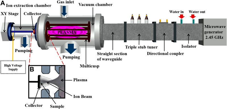
The experimental set-up, shown in Figure 1, comprises of two regions the plasma production chamber and the ion extraction chamber. Microwaves of 2.45 GHz are launched from a magnetron (Alter–TMA20) connected with its power supply and controller (Richardson PM 740). The waves are passed through a metallic rectangular waveguide (WR 340) and a quartz window into the plasma chamber, and the power is maintained at 180 W for continuous mode of operation. A water-cooled isolator (ISO) protects the magnetron from the reflected power. The directional coupler (DC) measures the forward and reflected power of the microwaves. The triple stub tuner (TST) is used for matching the impedance of the magnetron to the plasma, so that maximum power can be transferred to the plasma. The plasma production region consists of a vacuum chamber (VC) of length 50 cm and diameter 20 cm and a magnetic multicusp (octupole) which is placed inside the VC for confinement of the plasma [24]. The ports in the VC are used for gas inlet, probe diagnostics, pressure gages, and venting. The amount of Ar gas entering VC is controlled by a mass flow controller (MKS1179A). The base pressure of VC is kept around
The samples are copper sheets (purity
The surface morphologies of pristine and irradiated samples are investigated by Zeiss scanning electron microscopy (SEM, Model-SUPRA40VP). Atomic force microscopy (AFM, Model-ASYELEC-01, Asylum Research) provides the evidence of change in surface roughness due to microstructure formation. The MFP: 3D classic atomic force microscopy (AFM) measurements are performed in air with n-type silicon cantilever coated with Ti-Ir. AFM and Kelvin probe force microscopy (KPFM) scans an area of 25 μm2 at different locations on the samples to account for all types of irregularities. The KPFM provides the local work function of the surface scanned.
X-ray photoelectron spectroscopy (XPS, Model-5000 Versa Probe II spectrometer, FEI Inc.) technique is employed for elemental analysis. The X-ray beam diameter is 200 μm and the average area over which the sample is probed is 1 mm2. The achieved energy resolution is
The digital picture and schematic diagram of the field emission setup is shown in Figure 2. The experiments are performed on both pristine and irradiated samples with developed microcones, at room temperature. The experiments and measurements which are performed at room temperature implied that no additional heating of the substrate is done externally. The substrate is copper, which is a good conductor and the heat generated gets transported away by conduction through the metallic rod handle and radiation. Moreover, we have also performed the experiment by breaking down the time period of irradiation in slots of four for 60 s each and still have observed no significant change in pattern formation. So, we have taken into account the fluence variation as the key factor in generating dense structures. The field emission experimental setup is a parallel plate configuration with gap distance of 2 mm, kept in high vacuum chamber having a base pressure of 1.33
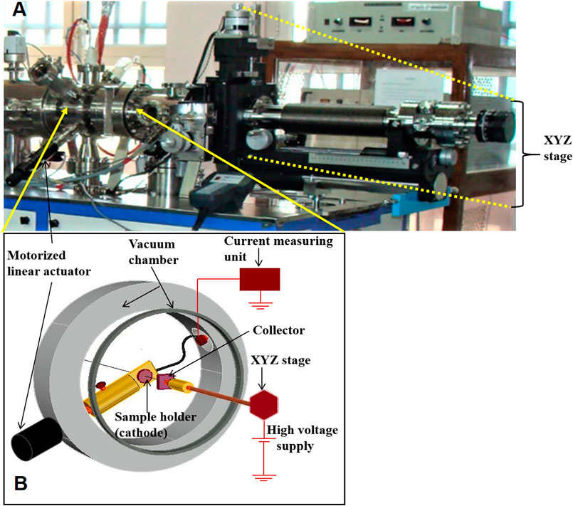
FIGURE 2. (A) Digital picture of experimental setup for field emission measurement experiment (not to scale); (B) the corresponding schematic diagram.
4 Experimental Results and Discussions
Figure 3 shows evenly distributed microstructures as observed from SEM analysis. In Figure 3A, we can see pristine copper with minute bright spots. The contrasting bright spots are initial random roughness generated due to HNO3 etching to remove the copper hydroxide layer which acts as a precursor of nucleation sites for stabilizing the growth process. Copper substrate exhibits high electrical conductivity, thermal conductivity, malleability, and ductility, which aids in easier structure formation for comparative analysis of field emission effects for a chosen range of fluences, when exposed to high electric field. In Figure 3B at a fluence of 1.3
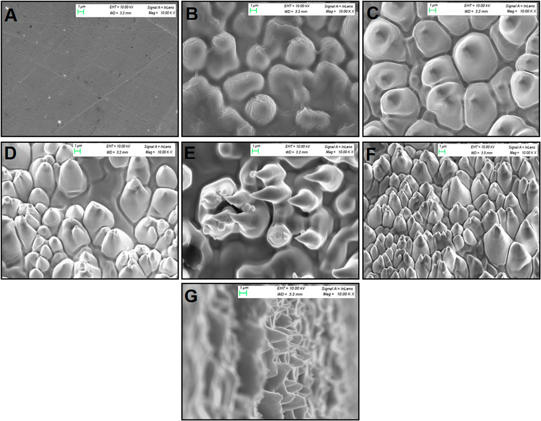
FIGURE 3. SEM images (10 μm
In Figure 4, the AFM and KPFM results are reported. The surface roughness variation of pristine and two of the exposed substrates at fluences of 3.2
where
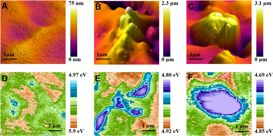
FIGURE 4. AFM topography (5 μm
Figure 5A shows high resolution spectra of argon with peaks at Ar 2p1/2 (
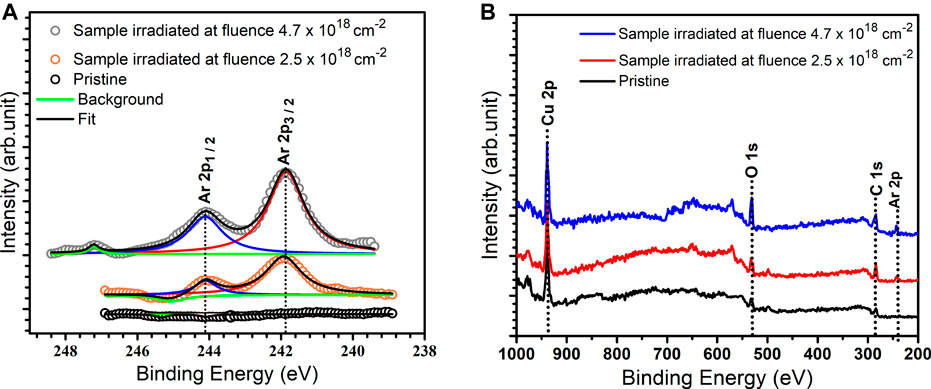
FIGURE 5. High-resolution X-ray photoelectron spectroscopy (XPS) spectra in (A) and X-ray photoelectron spectroscopy (XPS) survey spectra in (B) for two chosen argon-bombarded copper surface compared to pristine.
In Figure 6, the decrease in variation of work function distributed over the hillock (microconical tips) and valley (regions surrounding the microconical tips) regions, respectively, with the concentration of the implanted argon ions are plotted. The implanted argon concentration should increase with increase in time of exposure of the ion flux as the number of argon ions per unit area increases. The results obtained are consistent with this statement as they can be seen in Figures 5, 6. Argon implantation influence on the work function of metallic substrate is a comparatively new topic. A recent article aims at investigating the effect of particle irradiation on the work function in simple metals like Al and Zn using Ar+ ions at room temperature with 30 keV. The article uses similar KPFM technique and delves deep into understanding the theoretical aspects of the work function variation due to argon implantation [52].
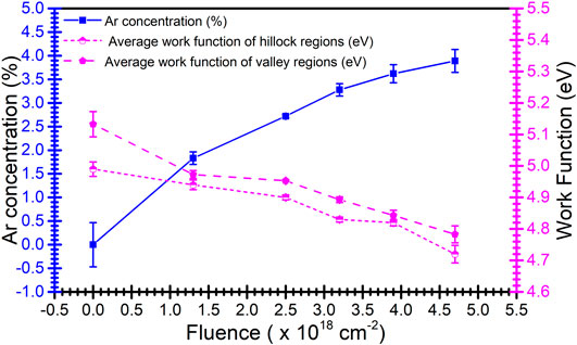
FIGURE 6. Variation of argon concentration (calculated from XPS data) and variation of the work function distributed over mounds (microhill regions) and relatively flat regions (obtained from KPFM data) with ion beam fluences.
The field emission experiment is performed using the micro conical structured substrates. The Fowler–Nordheim (FN) relation can be written in terms of the experimentally measured emission current (I) and applied voltage (V) as follows [53]:
where ϕ is the bulk work function (4.99 eV), d is the gap distance, S is the effective area, and A and B are constants as defined earlier in Eq. 1.
The characteristics of emission current versus applied voltage plot are shown in Figure 7A and the corresponding FN plot in Figure 7B. It is evident from the experimental data tabulated in Table 1 that there is a decrease in the work function with an increase in fluence. This is observed due to the formation of the atomically heterogeneous surface with increased production of uniformly aligned distinct micro conical tips as seen in Figure 3. Thus, the emission of electrons from these irradiated surfaces at a higher fluence is easier at a comparatively low applied voltage (turn-on voltage), as seen in Figure 7A. The turn-on voltage for substrate irradiated with a fluence of 4.7
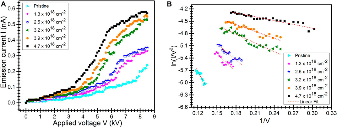
FIGURE 7. (A) Characteristics of field emission current (I) variation with the applied electric field (V) plot for individual fluences. (B) Fowler–Nordheim equation plot of pristine and irradiated Cu sheets by 2 keV argon ions beam. Voltage is measured in kilovoltage, while current is measured in nanoampere.

TABLE 1. A comparison of implanted argon concentration, work function variation with microcones distribution for pristine and irradiated samples.
The field enhancement factor is a morphology- and work function–dependent parameter, affecting the local field around micro (nano)-scale protrusions on the metal surface. There is a significant rise in steepness of the linear fitting on experimentally observed curves (and consequently the enhancement factor), with an increase in fluence.
As previously stated, the Fowler–Nordheim equation assumes a smooth planar metal surface with a given work function. But the observed work function gets modified due to both protrusion formation and subsurface implantation of argon ions causing a considerable change in the field emission properties of any ion irradiated substrate. Thus, assuming the bulk work function of substrate in calculating the field emission parameters particularly for irradiated samples may produce erroneous results. To explain our experimental results on field emission, we consider a parametric model to describe the field emission properties for atomically heterogeneous surfaces where the work function is taken to vary across the area encompassing both hilly and valley regions, implanted impurities, and structural deformities. We consider the effective work function to be a linear combination of the work function observed over the undulated surfaces. The parameters γ and δ are the effective proportions in which hillocks and valley areas are distributed for a particular substrate observed using images obtained after analysis from KPFM and SEM results. Using ImageJ software, the hilly regions obtained in digital scan are demarcated and isolated. The areal percentage is calculated from the pixel density and then, incorporated in their corresponding color coded regions to obtain the percentage of work function and aspect ratio contributions. ImageJ software is well-known software used to isolate digital image of cells in soft matter to calculate their areal percentage using pixel density difference of the image taken [54]. The effective work function thus becomes
which is employed in Eq. 3 in the place of ϕ and the β obtained is labeled as
In Figure 8A, the work function variation of both hillock-like and valley regions with aspect ratio is shown. The aspect ratio decreases with the increase in fluence with the formation of prominent and well-defined hillocks and valleys. The valleys are basically upturned conics where there is significant contribution from the nonuniform side of the slopes. Thus, the work function decreases for both hilly and valley regions leading to the extraction of electrons with ease and increase in the enhancement factor. In Figure 8B, the enhancement factor is plotted along with the aspect ratio as a function of ion beam fluence. The electron emission from these structures with low aspect ratio is relatively easy because of their pointed geometry and small radius of curvature. The generation of naturally selected absolute uniform sets of sub-microconical metallic arrays having each tip of similar height and base diameter is difficult. Hence, we have calculated the average aspect ratio for each of the irradiated samples. The aspect ratio is defined as ratio of the base width of the conical structure and its corresponding height, averaged over a number of such microprotrusions evaluated from the SEM analysis. The aspect ratio is found to be in the range of 0.7–1.5, implying low aspect ratio for pointed microstructures. The electrons can easily tunnel through such configuration with additional aid from the local surface charge developed in the vicinity of such structures. The presence of implanted argon ions may also influence the surface charge production significantly by causing variation in the enhancement factor. The modified enhancement factor
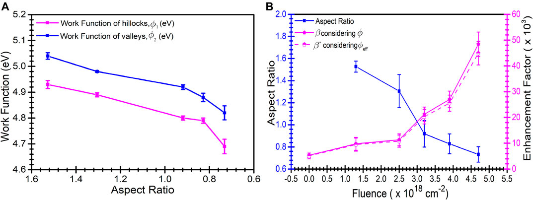
FIGURE 8. (A) Work function of both hillocks and valleys variation with aspect ratio. (B) Variation of aspect ratio and field enhancement factor (β and

TABLE 2. A comparison of aspect ratio of structures with turn on voltage and enhancement factor obtained considering bulk and modified work function, for pristine and irradiated samples.
5 Summary
In conclusion, the present study revisits sputter cones like structure with well-defined arrays of conical hillocks of micrometer dimension, challenging their requirements for seeded impurity atoms along with exploring their possibilities as promising field emitters. The growth mechanism of microconical arrays needs to be explored with a proper support from the substrate-oriented and modified existing theories in a channelized manner. The high enhancement factor of pristine is due to copper being a highly conductive metal, but the subsequent increase in the enhancement factor with field emission current for irradiated surfaces is because of the formation of atomically heterogeneous system (by low energy plasma ion irradiation) with multiple microprotrusions. The field emission results have shown almost eight times increase in the field enhancement factor for high fluence irradiation (4.7
Hence, there is a requirement for a relook at the existing FN theory for incorporating the effects of both the work function variation due to atomically heterogeneous surface and the corresponding field enhancement at the microconical tips. As a future work, it would be helpful to distinguish between the contribution of surface structure formation and heterogeneity introduction separately on the increase in field emission parameters. Experimental techniques aimed at masking the geometric effects of micro protrusions on field enhancement factor so that the effect of atomically heterogeneous surface layer influencing the field emission parameters that is discernible may be devised. A theoretical model based on understanding of the individual contribution of the parameters obtained from the experimental results and analysis, where a statistical distribution of arrays of microconics may be considered on a pure copper substrate. These microconical arrays with randomly distributed implanted inert gas ions will then represent the irradiated substrate for a comparative study with the experimentally obtained results.
Data Availability Statement
The original contributions presented in the study are included in the article, and further inquiries can be directed to the corresponding authors.
Author Contributions
JM and SB: designed and carried out the experiments, analyzed the experimental results, and wrote the manuscript. All authors contributed to the article and approved the submitted version.
Conflict of Interest
The authors declare that the research was conducted in the absence of any commercial or financial relationships that could be construed as a potential conflict of interest.
Acknowledgments
JM and SB gratefully acknowledge Mr. Omprakash and his colleagues of Physics workshop, IIT Kanpur for helping with the design and fabrication. We acknowledge fruitful discussions with Prof. John H. Booske, UW-Madison, United States. We thank Prof. Ashish Garg, for the AFM and KPFM measurements, the Centre of Nanosciences, for the SEM measurements and the Advanced Center for Materials Science (ACMS) for the XPS measurements (IIT Kanpur). JM thanks Dr. Dipak Bhowmik for introducing the Casa XPS software.
References
1. Heinig KH, Müller T, Schmidt B, Strobel M, Müller W. Interfaces under Ion Irradiation: Growth and Taming of Nanostructures. Appl Phys A: Mater Sci Process (2003) 77:17–25. doi:10.1007/s00339-002-2061-9
2. Chan WL, Chason E. Making Waves: Kinetic Processes Controlling Surface Evolution during Low Energy Ion Sputtering. J Appl Phys (2007) 101:121301. doi:10.1063/1.2749198
3. Albrecht M, Christiansen S, Michler J, Dorsch W, Strunk HP, Hansson PO, et al. Surface Ripples, Crosshatch Pattern, and Dislocation Formation: Cooperating Mechanisms in Lattice Mismatch Relaxation. Appl Phys Lett (1995) 67:1232–4. doi:10.1063/1.115017
4. Kajita S, Yoshida T, Kitaoka D, Etoh R, Yajima M, Ohno N, et al. Helium Plasma Implantation on Metals: Nanostructure Formation and Visible-Light Photocatalytic Response. J Appl Phys (2013) 113:134301. doi:10.1063/1.4798597
5. Zhu J-h., Brunner K, Abstreiter G. Two-dimensional Ordering of Self-Assembled Ge Islands on Vicinal Si(001) Surfaces with Regular Ripples. Appl Phys Lett (1998) 73:620–2. doi:10.1063/1.121875
6. Chang T, Kunuku S, Sankaran KJ, Leou K-C, Tai N, Lin I-N. Enhancing the Stability of Microplasma Device Utilizing diamond Coated Carbon Nanotubes as Cathode Materials. Appl Phys Lett (2014) 104:223106. doi:10.1063/1.4881419
7. Liu J, Zeng B, Wu Z, Zhu J, Liu X. Improved Field Emission Property of Graphene Paper by Plasma Treatment. Appl Phys Lett (2010) 97:033109. doi:10.1063/1.3467042
8. Lam S-T. Overview of Field-Emission Information Storage Devices. J Vac Sci Technol B (2003) 21:479–82. doi:10.1116/1.1541603
9. Egorov N, Sheshin E. Field Emission Electronics. Cham: Springer (2017). doi:10.1007/978-3-319-56561-3
10. Kuznetzov AA, Lee SB, Zhang M, Baughman RH, Zakhidov AA. Electron Field Emission from Transparent Multiwalled Carbon Nanotube Sheets for Inverted Field Emission Displays. Carbon (2010) 48:41–6. doi:10.1016/j.carbon.2009.08.009
11. Jin F, Beaver A. High Thermionic Emission from Barium Strontium Oxide Functionalized Carbon Nanotubes Thin Film Surface. Appl Phys Lett (2017) 110:213109. doi:10.1063/1.4984216
12. Han JS, Bredow T, Davey DE, Yu AB, Mulcahy DE. The Effect of Al Addition on the Gas Sensing Properties of Fe2O3-Based Sensors. Sensors Actuators B: Chem (2001) 75:18–23. doi:10.1016/S0925-4005(00)00688-2
13. Xu CX, Sun XW, Chen BJ. Field Emission from Gallium-Doped Zinc Oxide Nanofiber Array. Appl Phys Lett (2004) 84:1540–2. doi:10.1063/1.1651328
14. Gohel A, Chin KC, Zhu YW, Sow CH, Wee ATS. Field Emission Properties of N2 and Ar Plasma-Treated Multi-wall Carbon Nanotubes. Carbon (2005) 43:2530–5. doi:10.1016/j.carbon.2005.05.003
15. Tsai W-C, Wang S-J, Chang C-L, Chen C-H, Ko R-M, Liou B-W. Improvement of Field Emission Characteristics of Tungsten Oxide Nanowires by Hydrogen Plasma Treatment. Europhys Lett (2008) 84:16001. doi:10.1209/0295-5075/84/16001
16. Tanyeli İ, Marot L, van de Sanden MCM, De Temmerman G. Nanostructuring of Iron Surfaces by Low-Energy Helium Ions. ACS Appl Mater Inter (2014) 6:3462–8. doi:10.1021/am405624v
17. Zhang K, Bobes O, Hofsäss H. Designing self-organized nanopatterns on si by ion irradiation and metal co-deposition. Nanotechnology (2014) 25:085301. doi:10.1088/0957-4484/25/8/085301
18. Kim TC, Ghim C-M, Kim HJ, Kim DH, Noh DY, Kim ND, et al. Kinetic Roughening of Ion-Sputtered Pd(001) Surface: Beyond the Kuramoto-Sivashinsky Model. Phys Rev Lett (2004) 92:246104. doi:10.1103/PhysRevLett.92.246104
19. Ozaydin G, Özcan AS, Wang Y, Ludwig KF, Zhou H, Headrick RL, et al. Real-time x-ray studies of Mo -seeded Si nanodot formation during ion bombardment. Appl Phys Lett (2005) 87:163104. doi:10.1063/1.2099521
20. McCracken GM. A Review of the Experimental Evidence for Arcing and Sputtering in Tokamaks. J Nucl Mater (1980) 93-94:3–16. doi:10.1016/0022-3115(80)90299-8
21. You JB, Zhang XW, Cai PF, Dong JJ, Gao Y, Yin ZG, et al. Enhancement of Field Emission of the Zno Film by the Reduced Work Function and the Increased Conductivity via Hydrogen Plasma Treatment. Appl Phys Lett (2009) 94:262105. doi:10.1063/1.3167301
22. Zheng Z, Liao L, Yan B, Zhang JX, Gong H, Shen ZX, et al. Enhanced Field Emission from Argon Plasma-Treated Ultra-sharp α-Fe2O3 Nanoflakes. Nanoscale Res Lett (2009) 4:1115–9. doi:10.1007/s11671-009-9363-1
23. Chatterjee S, Bhattacharjee S, Maurya SK, Srinivasan V, Khare K, Khandekar S. Surface Wettability of an Atomically Heterogeneous System and the Resulting Intermolecular Forces. Europhys. Lett. (2017) 118:68006. doi:10.1209/0295-5075/118/68006
24. Chowdhury A, Bhattacharjee S. Localized Subsurface Modification of Materials Using Micro-low-energy Multiple Ion Beamlets. AIP Adv (2011) 1:042150. doi:10.1063/1.3664753
25. Singh KP, Majumdar J, Bhattacharjee S. Tuning Optical Properties of Atomically Heterogeneous Systems Created by Plasma-Based Low-Energy Ion Beams. Appl Opt (2020) 59:4507–16. doi:10.1364/AO.390751
26. Ritter M, Stindtmann M, Farle M, Baberschke K. Nanostructuring of the Cu(001) Surface by Ion Bombardment: a STM Study. Surf Sci (1996) 348:243–52. doi:10.1016/0039-6028(95)01024-6
27. Feng L, Yan H, Li H, Zhang R, Li Z, Chi R, et al. Excellent Field Emission Properties of Vertically Oriented Cuo Nanowire Films. AIP Adv (2018) 8:045109. doi:10.1063/1.5022320
28. Evangelakis GA, Papanicolaou NI. Adatom Self-Diffusion Processes on (001) Copper Surface by Molecular Dynamics. Surf Sci (1996) 347:376–86. doi:10.1016/0039-6028(95)00991-4
29. Zhu YW, Moo AM, Yu T, Xu XJ, Gao XY, Liu YJ, et al. Enhanced Field Emission from O2 and CF4 Plasma-Treated Cuo Nanowires. Chem Phys Lett (2006) 419:458–63. doi:10.1016/j.cplett.2005.11.087
30. Schäfer C, Gollmer DA, Horrer A, Fulmes J, Weber-Bargioni A, Cabrini S, et al. A Single Particle Plasmon Resonance Study of 3d Conical Nanoantennas. Nanoscale (2013) 5:7861–6. doi:10.1039/C3NR01292A
31. Camarero J, Cros V, Capitán MJ, Álvarez J, Ferrer S, Niño MA, et al. Epitaxial Growth of Metals with High Ehrlich-Schwoebel Barriers and the Effect of Surfactants. Appl Phys A: Mater Sci Process (1999) 69:553–7. doi:10.1007/s003390051469
32. Martynenko YV, Nagel’ MY. Model of Fuzz Formation on a Tungsten Surface. Plasma Phys Rep (2012) 38:996–9. doi:10.1134/S1063780X12110074
33. Bradley RM, Harper JME. Theory of Ripple Topography Induced by Ion Bombardment. J Vacuum Sci Technology A: Vacuum, Surf Films (1988) 6:2390–5. doi:10.1116/1.575561
34. Cuerno R, Barabási A-L. Dynamic Scaling of Ion-Sputtered Surfaces. Phys Rev Lett (1995) 74:4746–9. doi:10.1103/PhysRevLett.74.4746
35. Wehner GK, Hajicek DJ. Cone Formation on Metal Targets during Sputtering. J Appl Phys (1971) 42:1145–9. doi:10.1063/1.1660158
36. Wehner GK. Cone Formation as a Result of Whisker Growth on Ion Bombarded Metal Surfaces. J Vacuum Sci Technology A: Vacuum, Surf Films (1985) 3:1821–35. doi:10.1116/1.573386
37. Robinson RS, Rossnagel SM. Ion‐beam‐induced Topography and Surface Diffusion. J Vacuum Sci Technology (1982) 21:790–7. doi:10.1116/1.571826
38. Davidovitch B, Aziz MJ, Brenner MP. On the Stabilization of Ion Sputtered Surfaces. Phys Rev B (2007) 76:205420. doi:10.1103/PhysRevB.76.205420
39. Bradley RM. Theory of Nanodot and Sputter Cone Arrays Produced by Ion Sputtering with Concurrent Deposition of Impurities. Phys Rev B (2011) 83:195410. doi:10.1103/PhysRevB.83.195410
40. Perkinson JC, Anzenberg E, Aziz MJ, Ludwig KF. Model-independent Test of the Truncated Crater Function Theory of Surface Morphology Evolution during Ion Bombardment. Phys Rev B (2014) 89:115433. doi:10.1103/PhysRevB.89.115433
41. Fowler RH, Nordheim L. Electron Emission in Intense Electric fields. Proc R Soc Lond Ser A, Containing Pap a Math Phys Character (1928) 119:173–81. doi:10.1098/rspa.1928.0091
42. Kajita S, Ohno N, Hirahata Y, Hiramatsu M. Field Emission Property of Nanostructured Tungsten Formed by Helium Plasma Irradiation. Fusion Eng Des (2013) 88:2842–7. doi:10.1016/j.fusengdes.2013.05.014
43. Kyritsakis A, Xanthakis JP. Derivation of a Generalized Fowler-Nordheim Equation for Nanoscopic Field-Emitters. Proc R Soc A (2015) 471:20140811. doi:10.1098/rspa.2014.0811
44. Biswas D, Ramachandran R. Curvature Correction to the Field Emission Current. J Vacuum Sci Technology B (2019) 37:021801. doi:10.1116/1.5064403
45. Kildemo M, Calatroni S, Taborelli M. Breakdown and Field Emission Conditioning of Cu, Mo, and W. Phys Rev ST Accel Beams (2004) 7:092003. doi:10.1103/PhysRevSTAB.7.092003
46. Djurabekova F, Ruzibaev A, Holmström E, Parviainen S, Hakala M. Local Changes of Work Function Near Rough Features on Cu Surfaces Operated under High External Electric Field. J Appl Phys (2013) 114:243302. doi:10.1063/1.4856875
47. Toijala H, Eimre K, Kyritsakis A, Zadin V, Djurabekova F. Ab Initio calculation of Field Emission from Metal Surfaces with Atomic-Scale Defects. Phys Rev B (2019) 100:165421. doi:10.1103/PhysRevB.100.165421
48. Chowdhury A, Chatterjee S, Dutta A, Bhattacharjee S. Stopping Potential and Ion Beamlet Control for Micro-resistive Patterning through Sub-debye Length Plasma Apertures. AIP Adv (2014) 4:127127. doi:10.1063/1.4904371
49. Chowdhury A, Bhattacharjee S. Micron-focused Ion Beamlets. J Appl Phys (2010) 107:093307. doi:10.1063/1.3371688
50. Maurya SK, Barman S, Paul S, Bhattacharjee S. Charge Dissipation and Self Focusing Limit in High Current Density Ion Beam Transport through a Micro Glass Capillary. J Phys D: Appl Phys (2018) 52:055205. doi:10.1088/1361-6463/aaef4b
51. Frost F, Fechner R, Ziberi B, Völlner J, Flamm D, Schindler A. Large Area Smoothing of Surfaces by Ion Bombardment: Fundamentals and Applications. J Phys Condens Matter (2009) 21:224026. doi:10.1088/0953-8984/21/22/224026
52. Horváth Á, Nagy N, Vértesy G, Schiller R. Phenomenology of the Effect of Ion Irradiation on the Work Function of Metals. Nucl Instr Methods Phys Res Section B: Beam Interactions Mater Atoms 466 (2020) 12–6. doi:10.1016/j.nimb.2020.01.004
53. Bhattacharjee S, Vartak A, Mukherjee V. Experimental Study of Space-Charge-Limited Flows in a Nanogap. Appl Phys Lett (2008) 92:191503. doi:10.1063/1.2928232
Keywords: ion beam irradiation, microconical arrays, atomically heterogeneous surfaces, field emission, enhancement factor
Citation: Majumdar J and Bhattacharjee S (2021) Microconical Structure Formation and Field Emission From Atomically Heterogeneous Surfaces Created by Microwave Plasma–Based Low-Energy Ion Beams. Front. Phys. 9:674928. doi: 10.3389/fphy.2021.674928
Received: 02 March 2021; Accepted: 17 May 2021;
Published: 08 June 2021.
Edited by:
Agnes Granier, UMR6502 Institut des Matériaux Jean Rouxel (IMN), FranceReviewed by:
Dmitry Levko, Esgee Technologies, United StatesLuc Stafford, Université de Montréal, Canada
Copyright © 2021 Majumdar and Bhattacharjee. This is an open-access article distributed under the terms of the Creative Commons Attribution License (CC BY). The use, distribution or reproduction in other forums is permitted, provided the original author(s) and the copyright owner(s) are credited and that the original publication in this journal is cited, in accordance with accepted academic practice. No use, distribution or reproduction is permitted which does not comply with these terms.
*Correspondence: Jayashree Majumdar, jaymaj@iitk.ac.in; Sudeep Bhattacharjee, sudeepb@iitk.ac.in
 Jayashree Majumdar