 Yixiong Yan
94% of researchers rate our articles as excellent or good
Learn more about the work of our research integrity team to safeguard the quality of each article we publish.
Find out more
REVIEW article
Front. Phys., 12 May 2021
Sec. Optics and Photonics
Volume 9 - 2021 | https://doi.org/10.3389/fphy.2021.669591
This article is part of the Research TopicLaser Beam Shaping and Structuring: Techniques and CharacterizationView all 5 articles
In the past 20 years, semiconductor lasers have been widely used in medical, industrial, and communication applications, providing a revolutionary and powerful platform for the fifth generation and advanced manufacturing. Semiconductor laser has the advantages of small size, lightweight, high reliability and easy modulation, becoming increasingly popular. However, due to the laser diode emission mechanism limitation, the beam quality is inferior and cannot be directly applied and required to be handled by beam shaping. However, the packaging of multiple beam shaping optical components is accompanied by risks due to misalignment. The misalignment error of the optical components has a great hidden danger to the laser performance. As semiconductor lasers' power gradually increases, lasers' thermal management technology is also increasingly strict. Therefore, this article first reviews the beam shaping technology of semiconductor laser diode array. Secondly, the analysis of the influence of the array semiconductor laser optical device's misalignment is reviewed, and a feasible solution is proposed. Finally, it summarizes the researches on thermal management in high-power semiconductor lasers. This article aims to give readers a comprehensive and broad understanding of semiconductor laser packaging's technical difficulties and to recognize each corresponding solution.
Since the first semiconductor laser's birth in the 1960s, high-output-power, high reliability, and small volume are always the goals of the semiconductor laser. After 40 years of development, their performance has been dramatically improved. High power semiconductor laser diode (HPLD) has gradually become an essential core component in a wide range of fields, specifically, the modern laser material processing, laser remanufacturing, medical, and national defence-security fields. Figure 1 shows different semiconductor laser applications and application parameters.
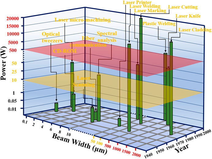
FIGURE 1. Statistics of applications of the semiconductor laser.
In the optoelectronics field, semiconductor lasers have become the mainstream of contemporary communication technology and are the only practical light source for optical fiber communication systems. Moreover, semiconductor lasers are widely used in optical disk storage, and their storage density is much greater than traditional storage methods. The spectral analysis of far-infrared tunable semiconductor lasers can analyze environmental gases and monitor atmospheric pollution. The semiconductor lasers are also universally used in laser alarms, laser printers and laser TV [1]. In the field of material processing, kilowatt-level high-power semiconductor lasers have been maturely used in metal cutting. It can also achieve high-speed and high-quality welding morphology in metal welding applications for the automobile industry's production process. Laser cladding is another specialty for the high-power semiconductor laser, reduces powder doping and lower heat input, can further improve the cladding process's economic benefits [2]. In the medical field, semiconductor lasers can be used as laser scalpels for precise and efficient cutting, and the wound healing speed will be faster than traditional scalpel cutting. It is also used in selective photothermal therapy. This technology uses nanomaterials to mark tumor cells and then uses semiconductor lasers to generate local high temperature to treat tumors accurately. Simultaneously, in medical treatments such as plastic surgery, ophthalmology, and physical therapy, the application of semiconductor lasers is also brilliant [3]. In the military field, semiconductor lasers can be used for laser guidance, laser ranging, lidar and even high-energy laser weapons. Its small size, high power, high efficiency, and good infrared band concealment make it the most competitive military laser light source [4].
The application of semiconductor laser has grown in popularity, which also poses an increasing challenge to its output performance requirements. At present, mainly two types of pump sources for high-power semiconductor lasers commonly are used in the market, single-emission type and bar-emission type. However, both of them are difficult to meet the application requirements directly due to the poor beam quality. As shown in Figure 2, the optical parameter is unbalanced in the fast and slow axis directions. Moreover, there is intrinsic astigmatism, and the far-field distribution of the beam is an elliptical spot. It is difficult to directly coupled into the fiber for applications. For semiconductor laser diode array (LDA), this issue is amplified [1].
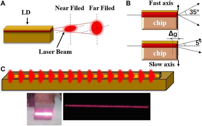
FIGURE 2. Luminescence mechanism and disadvantage of laser diode array: (A) Light field distribution diagram of laser diode; (B) Optical parameter unbalanced at two directions and astigmatism; (C) Luminous condition of laser diode array. Adapeted from [1].
With the increasingly sophisticated application fields, laser power and beam output quality requirements are further increased. The demand for kilowatt-level high-power semiconductor lasers has grown rapidly. Neither a single-emitter source nor bar emitter source can achieve such a large power output. Therefore, light sources are usually superimposed in the array form to increase the output energy. For a single-emitter array semiconductor laser source, multiple emitters are typically arranged horizontally for packaging. Moreover, a bar-array semiconductor laser source is usually packaged longitudinally with multiple bars. Regardless of the packaging form, as far as the pump source's light-emitting mechanism is concerned, the beam first needs to be collimated for compressing the divergence angle in the fast axis and slow axis. For single-emitter array semiconductor lasers, multiple beams need to be combined into one beam by beam shaping. For bar array semiconductor lasers, beam splitting and recombination are required to balance the beam's optical parameters in two directions. The beam shaping technology enables the beam spot size and divergence angle of the pumped beam to meet the conditions for efficient coupling into the optical fiber before it can be further applied [5]. For different light source parameters, the beam shaping optical device's surface shape and packaging position are specific. The optical beam shaping device manufactured with a diffraction-limited tolerance design can ignore the influence of surface tolerance. However, the load caused by the assembly, temperature changes, or structure generates misalignment of the optical device is inevitable. These optical devices' misalignment can cause changes in beam parameters such as spot size, divergence angle, and even optical path. It may make the beam shaping effect unable to achieve the desired effect, which badly affects the laser's output performances [6]. Semiconductor lasers are not only required to have high-power output, compact structure and lightweight design are also key technical requirements, which undoubtedly increases the pressure on laser heat dissipation technology. Due to the laser's pyroelectric effect and the beam's thermal radiation, it won't be easy to maintain an excellent working temperature for a multi-kilowatt laser. The high temperature has a severe impact on the threshold current, electro-optical conversion rate, central wavelength, output power and service life of high-power array semiconductor lasers. Besides, most of the reasons for the misalignment mentioned before are also caused by the laser's high temperature. Therefore, if the laser's high-performance output and high reliability are guaranteed, advanced heat dissipation solutions are also required to be equipped on high-power array semiconductor lasers [1].
Regarding the issues of semiconductor laser packaging, this article focuses on the following aspects: beam shaping technology of semiconductor lasers, the influence and prevention of optical device misalignment of semiconductor lasers, and thermal management of high-power semiconductor lasers. The contents of these three parts will be shown in Beam Shaping Technology Research, Optical Component Misalignment Research and Thermal Management, respectively.
The previous introduction shows that the semiconductor laser beam quality is poor, has a large divergence angle and asymmetric far-field, and needs to be improved by beam shaping technology before application. The following content first gives a detailed overview of the research into beam collimation technology. Besides, the study on beam combining and beam splitting and reshaping methods corresponding to single-emitter array semiconductor lasers and bar array semiconductor lasers are summarized.
Generally speaking, the collimation of a semiconductor laser is divided into two steps. In the first stage, the beam is collimated along the fast axis and then collimated along the slow axis. The most persistent FAC (fast axis collimator) include “D” type cylindrical lenses, “O” type cylindrical lenses and reverse “D” type cylindrical lenses. The principle and surface shape of SAC (slow-axis collimator) is similar to the FAC, except that the beam is compressed in the slow-axis direction, which makes the size and installation direction of the SAC is different from the former. Both lenses need to be optimized in size and curvature radius according to different applications to achieve beam collimation [1].
In addition to common cylindrical lenses, increasingly new collimators have been developed. These collimators not only have better collimation effects but are also easy to manufacture and package. Cao et al. proposed a method of making aspheric collimator at a meagre cost. They used UV (ultraviolet)-cured negative photoresist to make droplets on a specially designed substrate and controlled its surface shape by electrostatic force. It is cured into the best form that meets the design requirements. The schematic diagram of lens production is shown in Figure 3A. This aspherical collimator can compress the beam's fast axis's divergence angle direction to 3 mrad with cheap production cost [7]. Luo et al. designed an ellipsoidal collimator, made of epoxy resin, which can effectively collimate the irradiance distribution and reduce the beam's fast-axis divergence angle to less than 1°. It can be directly packaged on the laser diode, simplifying the manufacturing process and significantly reducing the size of shaping system. The schematic diagram of the lens package is shown in Figure 3B [8]. Besides, Xiong et al. proposed a design method for a variable curvature radius SAC suitable for a semiconductor laser bar, which can compress the slow axis's divergence angle to 6 mrad. The schematic diagram of the SAC surface is shown in Figure 3C. The most significant feature of this new type of SAC is that it can be applied to different light source parameters. Compared with other collimators designed for specific light sources, it has a broader range of applications and can reduce manufacturing cost [9].
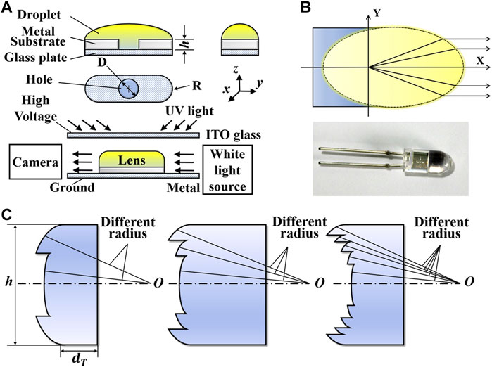
FIGURE 3. Innovative collimators: (A) Manufacturing method of UV curing adhesive collimator. Adapted from [7]; (B) Model and packaging form of the ellipsoidal collimating lens. Adapted from [8]; (C) Variable curvature radius SAC with the different number of divisions. Adapted from [9].
Integrated collimators have been designed to collimate the semiconductor laser beam on both the fast axis and the slow axis, simplifying the beam collimation system and reducing the lens package. Among them, Liu et al. designed an integrated collimator for array semiconductor laser beam collimation. It combined the FAC and SAC array into one part. The structure is shown in Figure 4A. This design diminishes the problem of too many array semiconductor laser beam shaping lenses, thereby significantly cutting the probability of packaging errors [10]. Then Tian et al. proposed a dual-axis hyperboloid micro-collimator made by femtosecond laser direct writing technology, which makes the fast-axis divergence and slow-axis divergence of a single-emitter laser beam can be collimated by a single lens. It can effectively compress the beam divergence angle of the fast and slow axes from 60° to 9° to 6.9 mrad and 32.3 mrad, respectively. The schematic diagram of the structure is shown in Figure 4B. This design is simple to manufacture, avoids multiple reflections and absorptions of the beam at multiple collimators, and further minimizing the packaging errors [11]. The collimator for semiconductor laser diode array designed by Wang et al. combines the above two technologies' advantages. The array beam can be collimated through one array biaxial hyperboloid collimator. The structure diagram is shown in Figure 4C, which undoubtedly minimizes the collimation system's packaging error [1].
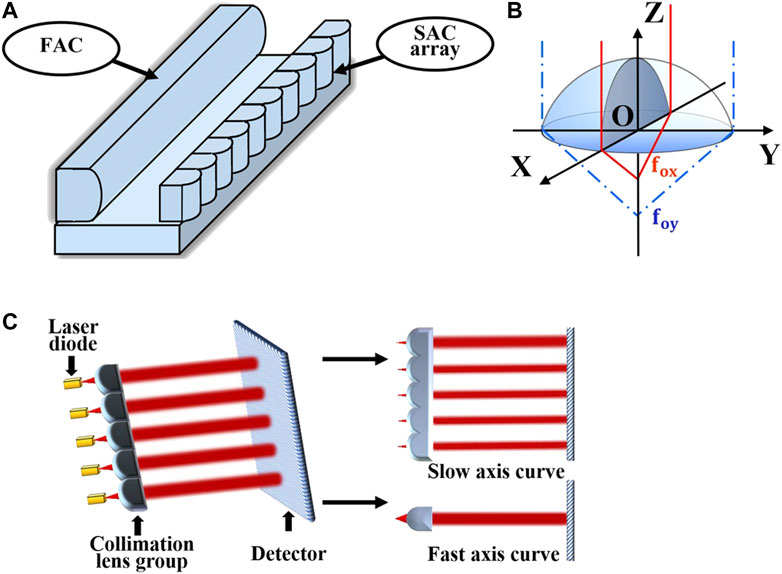
FIGURE 4. Various integrated collimating lenses: (A) FAC and SAC lenses combined into one optical device. Adapted from [10]; (B) One lens can collimate the divergence angle of a beam in two directions. Adapted from [11]; (C) One set of lenses can collimate the divergence angle of the Bar beams in two directions. Adapted from [1].
High-power single-emitter array semiconductor lasers are required to reduce the beam's size composed of multiple optical paths to maintain high output brightness while maintaining high output power. Therefore, the beam shaping system usually uses a spatial combination, polarization, and fiber bundle technologies to superimpose and combine multiple beams into one beam. Liu et al. arranged multiple single emitters sources in steps into a unit. The array beams emitted from 10 emitters with the same structure into one beam through 11 mirrors and a combined polarization beam combiner. Finally, the beam size is reduced and coupled into the optical fiber through the convergence system. The structure diagram is shown in Figure 5A. The laser composed of 50 emitters can output 1,900 W and be efficiently coupled into a 500 μm core fiber [1]. A high-power single-emitter array semiconductor laser with similar principles is designed by Leisher et al. The laser module comprises 56 emitters combined into two columns by polarization. The beam is symmetrical through a telescope, and finally focused by a multi-element objective lens. The structure diagram is shown in Figure 5B. Its output power can reach 500 W, the coupling fiber core diameter is 200 μm, and the photoelectric efficiency is greater than 60% [12].
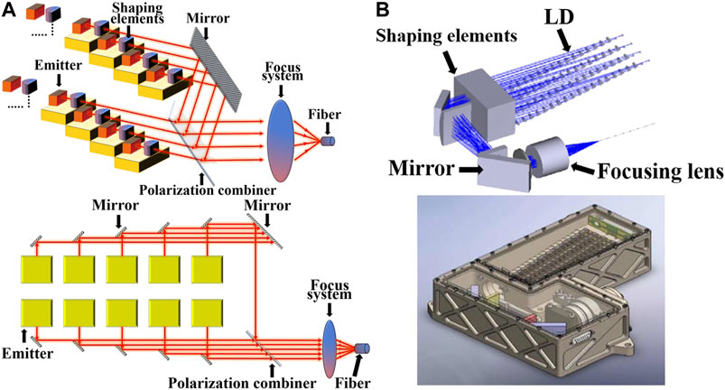
FIGURE 5. (A) Single-emitter based beam combining system using spatial and polarization superposition. Adapted from [1]; Beam combining system for 56 single-emitter array sources. Adapted from [12].
Unlike for single emitter pump, the Beam parameter product (BPP) of the bar pump in the fast axis direction and the slow axis direction is nearly 1,400 times different. In the first stage to improving its optical performance, the collimated bar beam is cut into N sub-beams, and were then rotated and recombined. So that the BPP in the fast axis direction is increased by N times, and the BPP in the slow axis direction is reduced by N times, which makes them balanced. The schematic diagram of the shaping principle is shown in Figure 6A [13]. According to this method, an increasing number of reorganization technologies have been continuously developed. Bonora et al. designed a small stepped lens for splitting and recombining the bar stack beam. It can couple a 200 W beam into a 300 μm fiber without losing brightness. The principle diagram of this structure is shown in Figure 6B [14]. Yu et al. designed a novel construction of segmentation and recombination system based on the building block step prism. It is composed of a trapezoid prism and a group of parallelogram plates. The schematic diagram of the structure is shown in Figure 6C. It couples 8 bar beams into a 200 μm optical fiber. The output power was 272 W and the coupling efficiency was 85% [15]. The beam combining system designed by Ghasemi et al. combined with beam polarization and spatial recombination technology can couple a 1 KW beam into a 365 μm fiber. The system consists of a strip mirror plate, a stepped mirror and polarization beam combining components. The schematic diagram of the structure is shown in Figure 6D [16]. Lin et al. used a polarized beam combiner to halve the beam size of two bar-stacked laser modules in the slow axis direction. And then the optical path reorganized by using a quartz plate stack on the fast axis to eliminate the beam gap area. In this way, the laser emitted by 12 bars can be coupled into an 800 μm fiber with a coupling efficiency of 87.5%, and the output power exceeds 1,400 W. The functional schematic diagram of the beam division and recombination system is shown in Figure 6E [17].
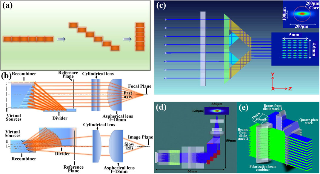
FIGURE 6. (A) Schematic diagram of beam splitting and reorganization. Adapted from [13]; (B) Side view and top view of the micro-step-mirror division and reorganization system. Adapted from [14]; (C) Schematic diagram of trapezoidal prism compressed beam. Adapted from [15]; (D) Schematic diagram of 1,000 W beam shaping system. Adapted from [16]; (E) Schematic diagram of beam combining of two stacked lasers with 1,400 W power. Adapted from [17].
The development of beam shaping technology has undoubtedly promoted the increasing advancement of array semiconductor lasers. The kilowatt semiconductor lasers with 100-micron fiber output expanded the upper limit of laser applications. Moreover, the laser with high coupling efficiency output realized by beam shaping technology saves the laser's application energy consumption while ensuring the laser's reliability. However, the participation of a large number of beam shaping devices is inevitable to maintain the high beam quality. Although scholars have made great efforts to simplify the structure and number of beam shaping devices, the effect is still not significant for the time being. Multiple optical device packages expand the volume of the entire laser, limiting some laser's application. Besides, in the laser packaging process, more optical devices' participation means more additional risk of packaging errors. This issue will also be discussed in the next section. Therefore, the optimization of the beam shaping system still has a long way to go.
As mentioned before, misalignments in the packaging process are unavoidable. Every additional optical device involved in shaping will have higher misalignment risks. This chapter aims to give the reader a comprehensive view of the field, recognizing the severity of the impact of misalignment. Firstly, the types and characteristics of semiconductor laser misalignment have introduced. Moreover, the research into the influence on the array semiconductor laser optical device’s misalignment is reviewed. Finally, the feasibility study of reducing the influence of misalignment is discussed.
For optical devices, misalignment can be divided into three categories: rotation misalignment, which also called tilt; linear offset from the optical axis, as known as the decenter; Linear offset along the optical axis, which also called defocus. As shown in Figure 7A. When the focused beam is irradiated on a plate with tilt, the beam’s focus position will be offset on the Y-axis and Z-axis. The offset on the Y-axis is d, and the offset on the Z-axis is g, as known as astigmatism. The size of astigmatism g mainly depends on the divergence angle u of the focused beam and the offset angle θ of the plate. The magnitude of the offset d also depends on the thickness and refractive index of the plate. The tilt on the focus lens will cause coma, which will significantly increase the spot size; As shown in Figure 7B. The decenter is the parallel relative displacement between the laser's optical axis and the lens's optical axis. Like tilt, the eccentricity will cause image coma, and deviate the beam from the optical axis. The optical devices decenter directly causes the focused beam to fail to be coupled into the optical fiber, which reduces the coupling efficiency. As shown in Figure 7C. Defocus refers to the offset of the detector or lens on the optical axis, resulting in a change in the axial relative distance between the detector and the optical shaping device, making the image blurred and the spot size larger. The expected optical effect cannot be obtained. These misalignments will raise the optical performances phenomenon such as aberration, astigmatism and distortion, which will lead to the attenuation of optical system performance [18–20].
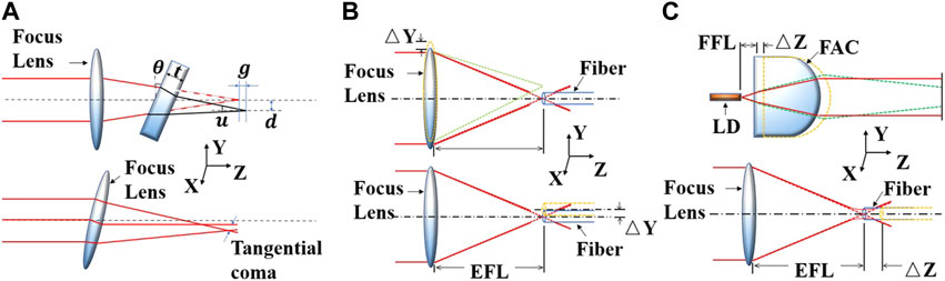
FIGURE 7. Types of optical components misalignment: (A) Tilt; (B) Decenter; (C) Defocus.
The previous section allows readers to understand the various optical phenomena caused by different misalignments of optical devices, and what effects may be brought to the optical characteristics. This section will review the research results on the impact of misalignments on different laser optical components on laser output performance. The optical components studied include collimator, reflector, converging lens and fibers. Details will be shown in the following paragraphs.
Generally, the first stage of beam shaping process is collimation, and subsequent beam shaping processes are performed. Therefore, the study of collimator misalignment is significant. Zhou et al. studied the influence of stacking semiconductor laser FAC and SAC misalignment through simulation analysis. It shows that the linear error in the Y-axis direction of FAC and the rotation error in the X-axis direction have the greatest impact on the coupling efficiency [21]. Yan et al. conducted a quantitative study on the influence of the collimator misalignment. When the linear misalignment of FAC in Y-axis is 4μm, the optical coupling efficiency will drop by 80%. When the rotation misalignment in X-axis exists on the FAC is 0.5°, it will result in a 40% drop in coupling efficiency. They also used the ABCD matrix rule to calculate the evaluation equation of the collimator misalignment's influence on the laser intensity distribution [22]. Westphalen et al. established a beam propagation model based on wave optics. They deduced FAC misalignment's influence on the laser beam's power density distribution characteristics distortion in near-field and far-field. Moreover, based on the model and the influence relationship, a FAC automatic alignment algorithm was developed. It was found that the FAC process's performance aligned with this self-aligning algorithm was improved by 70%, and the linear misalignment was less than 0.8 μm. The angle misalignment is less than 0.01° [23].
Reflectors and converging lens are used for beam combination and spot size reduction of the laser beam, the precise alignment is also critical. For the reflector, Zhang et al. used the matrix equation method to analyze the influence of reflector misalignment and derived the relationship between misalignment and beam size [24]. Based on the former, Yan et al. studied the influence of the array semiconductor laser reflector's misalignment on the coupling efficiency through experiments. The results showed that the rotation misalignment existing on the reflector has a considerable influence on the coupling efficiency. 0.5° rotation misalignment will reduce the coupling efficiency by 95% [25]. For the converging lens, Qiao et al. analyzed the influence of the converging lens's misalignment on the coupling efficiency through simulation. The results show that the linear misalignment in the Y-axis direction is the most significant, followed by the linear misalignment in the Z-axis direction. The rotation misalignment has the least effect [26]. Yan et al showed that a 1.5 mm linear misalignment in the converging lens's Z-axis direction would reduce the beam spot roundness by 50% [27]. To reduce the influence of the converging lens's misalignment, Fadhali et al. designed a new type of converging lens set to achieve a high coupling efficiency of the laser even when there is a 1–4 mm misalignment [28].
Research into fiber misalignment is the hottest. In 1984, Joyce et al. analyzed the coupling design between any two optical devices supporting the Gaussian model. Moreover, they obtained the relational expressions between coupling efficiency and linear misalignment and rotational misalignment [29]. Tang et al. established a model of fiber misalignment based on the Monte Carlo method. They concluded that the most influential fiber misalignment is the rotation error [30]. Junhong et al. further quantitatively analyzed the influence of fiber misalignment on the coupling efficiency based on simulation analysis. They pointed out that when the fiber has a linear alignment tolerance of 80 μm in the Y-axis, the coupling efficiency drops by 75%. The 80 mrad angular misalignment that exists in the X-axis direction will lead the coupling efficiency to drops by 80% [31]. Based on experimental research, He et al. found that the fiber misalignment range that keeps the coupling efficiency above 50% is that the Z-axis linear misalignment is less than 582 μm, the Y-axis linear misalignment is less than 10.2 μm, and the rotation misalignment is less than 1.07° [32]. Kong et al. designed a graded-index planar waveguide coupler based on the theoretical model, increasing the fiber misalignment tolerance and making the coupling efficiency reach 99% [33].
Various methods have been used in these analyses, including theoretical calculation, experimental analysis and simulation analysis. Most studies have obtained the specific values of the influence of misalignment of beam shaping devices on the output performance of laser diode. The influence of optical device misalignment on the output performance of the laser is revealed. Among them, the collimating lens's linear error and the rotation error of the reflector are particularly fatal. The misalignment of other optical devices also should not be underestimated. Moreover, some of the researchers have also come up with solutions to improve the tolerance of optical devices, such as the design of new beam shaping devices and new couplers. However, limitations exist in these schemes; most of them expand the tolerance range of a single optical device and are unable to consider all devices.
As mentioned before, the misalignments of semiconductor laser optical devices are mainly caused by packaging errors, temperature changes or structural stress. Packaging errors are unavoidable due to the influence of human-made operating factors. The way to reduce the risk is to reduce the number of packaged components. The structural stress is related to the structural size and weight of the beam shaping device. For considering these two requirements, the first feasible solution is to use diffractive optics to design a beam shaping device to reduce packaging errors.
The traditional beam shaping device is mainly designed based on refraction and reflection, and most of the components are simple in structure and heavy. The beam-shaping lens designed by diffractive optics uses microelectronic processing technology to etch on the optical material substrate's surface. It presents embossed microstructures of different depths amplitude or phase of these microstructures' incident light field, various optical properties. Its thin and light characteristics are more suitable for the current optical system miniaturization, high integration and array requirements than the traditional optical plastic lenses. Usually, one diffractive shaping element can simultaneously realize the functions of multiple conventional shaping lenses. In theory, it can realize any irregular surface lens, break through the theoretical limit of traditional glass devices, and realize the optical functions that it is difficult to possess. It is an extremely effective technical method that can be applied to laser beam shaping. However, the shortcomings of diffractive optical elements are also undeniable. The difficulty of optical device design optimization is significantly increased. And limited by the technological level, it is currently unable to produce high-efficiency beam shaping components that can realize arbitrary wavefront transformation theoretically [34].
Generally, the optical shaping devices of semiconductor lasers are all bonded and packaged with UV adhesive. When the laser is working, the laser chip's temperature and the optical device rise sharply. The UV adhesive is deformed through heat conduction and thermal radiation, which causes the misalignment of the optical device [1]. Therefore, the second feasible solution is to reduce the UV adhesive's thermal deformation to lower the deviation of the misalignment of the optical device. According to the principle of thermal expansion, it can be known that objects will expand when the temperature rises. However, due to the different thermal properties between UV adhesive and optical lenses, this will generate more significant thermal stress, leading to thermal strain. Therefore, it can try to change the thermal properties of UV adhesive by adding quartz particles or other micro-nano materials with a thermal expansion coefficient close to that of the lens. It makes the lens and UV adhesive have similar thermal properties to reduce thermal stress and misalignment. However, this feasibility plan is still only an assumption, and its effect has not been tested by practice. In contrast, it is more realistic to consider decreasing the generation of high temperatures to reduce the misalignments. The following chapter will summarize the efforts made by scholars in the research into semiconductor laser thermal management.
Although the photoelectric conversion efficiency of semiconductor lasers is far superior to other types of lasers, the requirements for their increasingly higher power and compact structures have significantly raised the strictness of their thermal management technology. High power density output will cause the laser to generate a considerable heat flux, seriously affecting its output performance, such as efficiency, power and wavelength, and reliability. The core factor of the misalignment mentioned above also points to this. Therefore, research into heat dissipation solutions for high-power semiconductor lasers is always prevalent. The thermal management technology of high-power semiconductor lasers introduced in this chapter is divided into the traditional heat dissipation method and new heat dissipation method. The heat dissipation methods and effects of various thermal management technologies are demonstrated, their advantages and disadvantages are analyzed, and the feasible heat dissipation schemes are finally discussed.
The natural convection cooling method uses high thermal conductivity metal to extend the natural convection heat dissipation area of the laser chip, increasing the heat dissipation and reducing the laser chip's temperature. This method's heat dissipation structure is easy to process and easy to assemble, and copper with high thermal conductivity is usually used as the heat sink material. Yuncu et al. designed a fin-type heat sink. The effect of the height and spacing of the fins on the heat dissipation effect is obtained through research. When the temperature is constant, the optimal fin spacing decreases as the fin height increases. The heat sink can be used for 50 W laser with high performance [35]. Meng et al. further studied the relative mounting angle of the similar fin-type heat sink and the chip on the heat dissipation performance. The research shows that the heat dissipation effect is the worst when the installation angle is 15°, and the heat dissipation effect is the best when the installation angle is 90°. It is also found that by appropriately cutting off the corners of the heat sink fins, and the specific thermal resistance can be reduced and the heat transfer coefficient improved. The heat sink can be used for 80 W laser with high performance. The heat sink structure and the temperature distribution of the fins under different installation angles are shown in Figure 8A [36]. However, the capacity of this type of heat dissipation method is limited, and the overall heat dissipation speed is relatively slow, which is only suitable for the early low-power semiconductor lasers. It is challenging to meet the requirements of high-power lasers with increasing power.
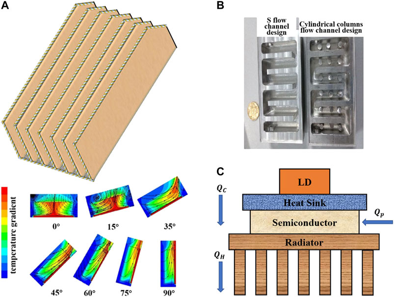
FIGURE 8. Tradition heat dissipation methods: (A) schematic of cut corner heat sink and temperature distribution of heat sink fins at different installation angles. Adapted from [36]; (B) S-type with cylindrical spoiler large channel water cooling device. Adapted from [38]; (C) Schematic diagram of typical semiconductor cooling device. Adapted from [40].
Scholars have transformed natural convection into forced convection by constructing a large-sized cavity in the heat sink and injecting water to further reduce the laser's high thermal load. This heat dissipation method is called the large-channel water cooling method. Which has higher heat dissipation efficiency than the passive heat dissipation method. The water-cooled heat dissipation channel designed by Kan et al. achieved higher laser photoelectric efficiency conversion by optimizing the aperture size. The radiator can ensure that the thermal resistance of the laser is 0.6°C/W when the output power is 115 W. However, this design has the problems of uneven temperature distribution and low heat flux [37]. Therefore, some scholars have proposed to add various turbulence structures in the water-cooled channel, such as in-line structure and cross-line structure, which increases the average heat flux density, but increases the channel pressure. Later, Zhao et al. designed an S-shaped water-cooled channel heat dissipation structure with cylindrical turbulence and determined the water flow speed for the best heat dissipation effect through research. The heat dissipation effect is better than the previous results. The thermal resistance is 0.015°C/W when the 200 W laser working. The heat dissipation device structure is shown in Figure 8B [38]. Moreover, Tsunekane et al. pointed out that the heat dissipation device with a microfiber structure on the water-cooled channel’s surface has a 40% lower thermal resistance than a planar structure [39]. The heat dissipation effect of the large-channel water cooling method is becoming more challenging to meet high-power lasers’ needs. However, its simple structure and good heat dissipation effect are among the most widely used heat dissipation methods in practical applications at this stage.
Semiconductor refrigeration is a heat dissipation method based on the Seebeck effect. In the semiconductor cooling process, the semiconductor refrigeration chip can only be used as a heat dissipation carrier, and it needs to consume electrical power. Finally, the heat needs to pass through the cold end and spread out in convection. The structure diagram is shown in Figure 8C [40]. As early as 1992, Tongeren et al. used this heat dissipation technology to maintain the laser chip temperature at 25°C when the ambient temperature is 65°C [41]. Moreover, Zhang et al. improved the semiconductor heat sink’s heat dissipation efficiency by increasing the heating section’s fluid flow rate and the size of the cooling fins. It shows that the when the ambient temperature is 60°C, the thermal resistance is less than 1.55°C/W [42]. Similarly, Tan et al. optimized the TEC structure. They improved the distribution of its heat transfer area. The heat exchanger area's ratio at the cold and hot ends of the TEC reached the best heat dissipation effect and found the relationship between the TEC material characteristics and the maximum heat dissipation efficiency [40]. This research has guiding significance for the design of semiconductor refrigeration system. The refrigeration method has a speedy heat dissipation rate and has the advantages of small size, high reliability, and simple operation. However, its cooling effect is limited, and it can usually only be used in low-power semiconductor laser cooling systems.
The micro-channel water cooling method is different from the traditional large-channel water cooling in two main points. The first point is that the channel's size is smaller, with a diameter of 10–200 μm; the second one is that its surface tension is greater. And the micro-channel cooling method has the advantages of lower cooling cost, less electrochemical corrosion damage and easy maintenance. Its typical structure is shown in Figure 9A [6]. To further improve the heat dissipation performance of the micro-channel water cooling device, simplify the manufacturing difficulty of the microchannel, and increase the feasibility of the design, scholars have made a lot of efforts to optimize the structural design of them. Kozlowska et al. designed a heat dissipation structure combining microchannels and microtubes, which is shown in Figure 9B. This design uses the slits between the microtubes and the channels as the heat exchange microchannels, reducing the processing of the microchannels. It can ensure that the laser has good heat transfer performance when the heat flux density is 380 W/cm2 [43]. However, this single-layer channel is prone to uneven temperature distribution. For this problem, Hung et al. designed a double-layer microchannel structure. This double-layer microchannel heat sink’s thermal resistance is smaller than that of a single-layer structure, with better heat dissipation and more uniform temperature distribution. The heat dissipation effect is 6.3% better than single layer one [44]. Wang et al. optimized the double-layer microchannel heat sink structure based on the former. They cut off the upper channel, and the heat sink structure was stepped. Such a heat sink has a 30% reduction in thermal resistance than the previous one [45]. Nevertheless, such a double-layer heat sink structure is challenging to process. Deng et al. designed a microchannel water-cooled heat sink composed of five copper plates with different structures. The schematic diagram of the structure is shown in Figure 9C. The first layer is used as the coolant inlet and outlet; the second, three and four layers are combined to construct a micro-slit channel. The last layer is used as a laser chip mounting substrate. Such a layered micro-channel structure can satisfy the double-layer channel structure and solve the problem of complicated processing. At the same time, they also studied the influence of the slit length setting on the heat dissipation effect, and the results showed that the longer the slit, the smaller the pressure drop, but the more significant the thermal resistance. At a flow rate of 0.8 L/min, the radiator’s heat flux can reach 506 W/cm2, and the thermal resistance is only 0.23 K/W. Generally, microchannel heat sinks use copper or silicon as the base material [46]. Goodson has made further improvements in the heat sink material, using materials with higher thermal conductivity. They designed and fabricated diamond microchannel heat sinks through CVD technology. Compared with microchannels made of silicon, diamond microchannels have lower enthusiasm and better heat dissipation characteristics. The thermal resistance is calculated to be 75% less than that of silicon made microchannel [47]. In general, the micro-channel water cooling method has shown significant advantages in applying high-power semiconductor lasers, which are manifested explicitly in high heat dissipation efficiency, small heat dissipation structure, low cooling cost. With the growing development of processing and manufacturing, increasing ingenious and high-efficient micro-channel heat sink designs have been made and applied. However, problems such as easy blockage of the channel and relatively high fabrication cost need to be further solved in its application.
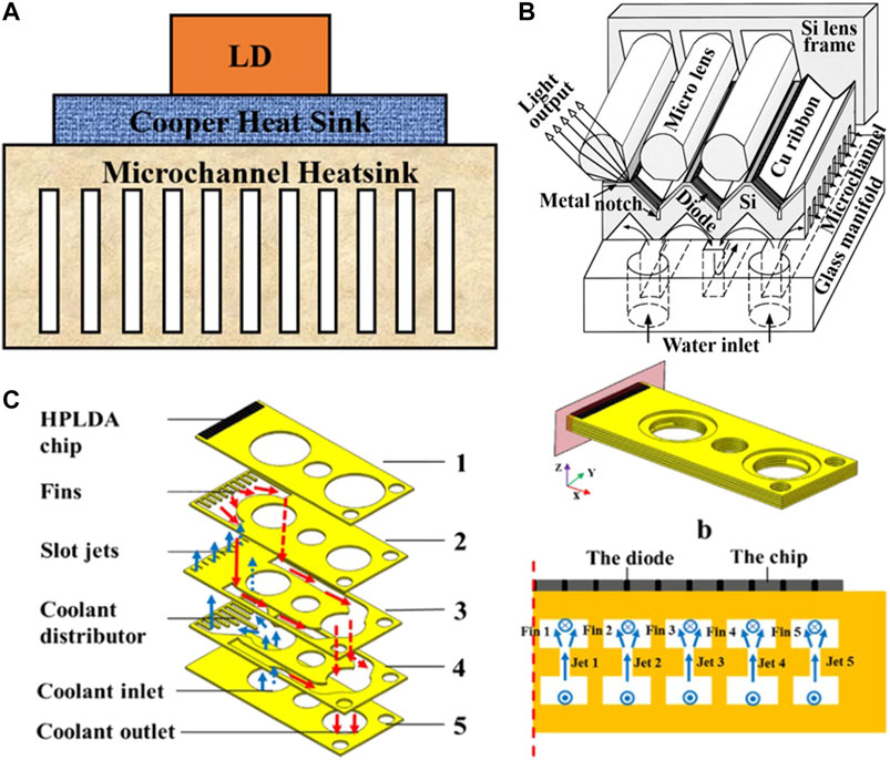
FIGURE 9. (A) Schematic diagram of typical microchannel heat dissipation device. Adapted from [6]; (B) The structural model of using gaps as heat exchange micro-channels. Adapted from [43]. (C) The detailed structure diagram of the microchannel water-cooled heat dissipation device composed of five layers of sheets. Adapted from [46].
Compared with the micro-channel heat dissipation method, the structure of the spray cooling device is more complicated. This method first atomizes the cooling liquid into a gas-liquid two-phase fluid with high pressure. Then forcibly sprays it to the heating surface, and finally through convection and phase change heat transfer to achieve efficient heat transfer enhancement. As early as 1992, Yang et al. used spray cooling to achieve a maximum heat flow density of 1,000 W/cm2 [48]. Later, Pais et al. further increased the heat flux density of spray cooling to 1,200 W/cm2 by strengthening the surface roughness [49]. Traditional spray cooling uses the vaporization heat absorption of droplets to achieve heat dissipation. Ishimoto et al. designed a spray cooling structure shown in Figure 10, which solidifies liquid nitrogen into nitrogen particles under the cooling of helium, and then uses nitrogen particles to cool the surface by its sublimation [50]. Bostanci et al. studied the influence of spray flow rate, spray distance, inlet fluid temperature and surfactants on heat transfer performance [51]. These studies on spray cooling parameters provided a basis for subsequent optimization. Spray cooling technology has significant advantages in heat dissipation with high heat flux, but its structure is complex, and there are specific difficulties in applying laser heat dissipation. Its main application areas are the nuclear power industry and the chemical industry. However, as the technology continues to mature, spray cooling devices that are more suitable for heat dissipation of high-power semiconductor lasers.
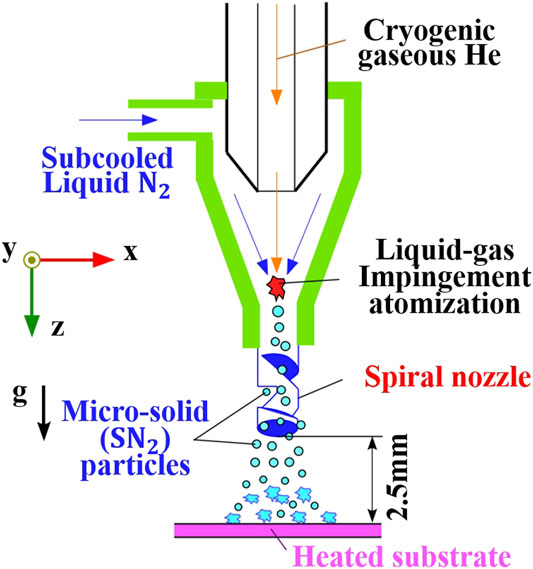
FIGURE 10. Nitrogen-fixing spray cooling device developed by Ishimoto. Adapted from [50].
Jet impingement heat dissipation is a heat dissipation method that uses high-speed fluid to impinge on the heat transfer surface to enhance heat transfer. Silverman et al. used liquid metal with a flow rate of 4 m/s to impact the heat dissipation surface to dissipate heat from a particle accelerator with a high heat flux density of 2,000 W/cm2. However, the heat exchange temperature difference reached 100°C [52]. Obviously, the heat sink is directly applied to the laser heat dissipation may cause some problems. By contrast, Browne et al. used water with a temperature of 23°C and a flow rate of up to 20 m/s as the jet medium to control the hot surface temperature with a heat flux of 1,100 W/cm2 at 50°C. The designed jet impact nozzle structure is shown in Figure 11A. This nozzle is made of microelectronic machinery precision processing. It has a compact structure and good reliability, which is suitable for the laser’s heat dissipation and can effectively solve the laser chip's smile effect [53]. Miyajima et al. designed a new type of jet impingement cooling radiator, which combines jet impact technology and water-cooling technology. The schematic diagram of the structure is shown in Figure 11B. The device consists of a water inlet, a heat exchanger and a water outlet. The cooling liquid flows through the bottom, and the cooling liquid injected through the 300 mm hole impacts the rough surface of the target plate to improve the cooling efficiency. The thermal resistance of the 255 W output laser can be controlled at 0.25°C/W [54]. The jet impingement cooling technology is usually applied to nuclear reactors' heat dissipation, and other superheat fluxes. The disadvantage of using this heat dissipation method is that a specific high-speed jet cooling medium needs to be provided, that the power consumption will be relatively large. It needs further optimization to apply it to the heat dissipation of high-power semiconductor lasers.
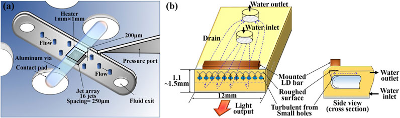
FIGURE 11. (A) Schematic diagram of nozzle structure of jet impact device suitable for laser heat dissipation. Adapted from [53]; (B) Schematic diagram of a device that combines water-cooling heat dissipation and jet impact heat dissipation. Adapted from [54].
Heat pipe heat dissipation is a passive heat dissipation device. It also uses phase change heat transfer to achieve heat dissipation. The typical heat dissipation structure is shown in Figure 12A. Hou et al. designed two heat pipe cooling devices. The first n-type heat pipe cooling system consists of eight 6 mm heat pipes and sintered powder wicks, which can easily handle a laser module’s heat loads of up to 73 W, with a maximum heat flux of 367 W/cm2. The second U-shaped heat pipe cooling system consists of ten 12 mm copper heat pipes and sintered powder wicks, which can easily handle five laser modules' heat loads of up to 300 W. The schematic diagram of the structure is shown in Figure 12B [55]. Some scholars have studied the influence of the inclination angle of the heat pipe and the filling rate on the heat transfer efficiency and found that when the filling rate is 30%, the heat pipe has a better heat transfer effect. The horizontal heat pipe has a smaller thermal resistance [56]. Although the heat pipe heat dissipation technology is a new type of laser heat dissipation scheme, the heat flux density it can achieve is not very high due to passive heat dissipation. The application of heat pipe heat dissipation technology for lasers is still in the preliminary stage of exploration, and further research is needed.
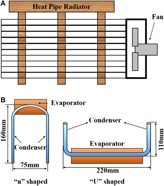
FIGURE 12. (A) Schematic diagram of typical heat pipe cooling device structure; (B) Structure diagram of U-type and n-type heat pipe radiator. Adapted from [55].
Liquid metal has good thermal conductivity. For example, the thermal conductivity of gallium-indium alloy is about 28 times that of water, and it has good convection heat transfer. Therefore, this material is widely used in electronic chip heat dissipation technology, and some scholars also use it in the heat dissipation of high-power semiconductor lasers. Vetrovec et al. creatively created a liquid metal heat dissipation method. They poured liquid aluminum alloy into the ring to rotate, and at the same time combined heat pipes or microchannels to dissipate heat. The structure diagram is shown in Figure 13A. Studies have shown that when the heat flux indicated by the laser chip reaches 1,000 W, the chip temperature is only 23°C [57]. Zhang et al. applied vascularized liquid metal cooling technology to the heat dissipation of high-power semiconductor laser diode array. A liquid metal radiator containing 70 channels with a size of 1.8 mm is designed. The experimental results show that liquid metal cooling can realize the heat dissipation of the 2,000W laser, and the top surface temperature of the radiator is lower than 54°C. Moreover, when the flow rate is faster than 2.4 L/min, vascularized liquid metal has better cooling than vascularized water cooling. The structure diagram is shown in Figure 13B [58]. Muhammad et al. studied the thermal characteristics and flowed properties of a microchannel heat sink using Gailnstan liquid alloy as a coolant. This integrated microchannel cooling and liquid metal cooling technology provide new ideas for developing new heat dissipation technologies for high-power semiconductor lasers [59]. Although liquid metal has good heat dissipation performance, it still has some problems as a coolant, such as corrosion between liquid metal and common metal. The cooling device cannot operate in a low-temperature environment. Further development of this technology is needed.
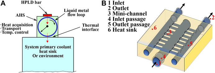
FIGURE 13. (A) Liquid metal heat dissipation system in which liquid aluminum alloy rotates in a ring tube to take away heat. Adapted from [57]; Structure schematic of vascularized liquid metal heat sink. Adapted from [58].
Scholars have put a lot of effort into optimizing laser heat dissipation technology to solve the problem of high thermal load of high-power semiconductor lasers. Most of the new heat dissipation methods have certain advantages in heat dissipation with high heat flux. However, most of them require complex design structures and complicated processing. For example, micro-channel water-cooling heat dissipation technology puts high demands on the precision processing of micro-channels. If a multi-layer format is used to form the channel, high-quality packaging technology must be achieved. In recent years, the TSV packaging technology, which has gradually become a hot spot, is expected to be applied to microchannel heat dissipation technology. Its high-precision and high-reliability characteristics can effectively solve traditional microchannel processing difficulties and effectively achieve high-density interconnections. However, TSV packaging technology usually uses silicon as the base material for the formation of holes. The silicon’s thermal conductivity is not as good as that of metal materials such as copper. This problem remains to be solved. As mentioned earlier, liquid metal heat dissipation needs to consider liquid metal and channel materials’ compatibility. The graphene material can solve this problem well. First of all, the material's thermal conductivity dramatically exceeds that of common liquid metals, and its stability is high, which is difficult to react with other metal materials. Therefore, it can be considered to add graphene micro-nano particles to the coolant as a new type of coolant for heat dissipation. However, the microchannel heat dissipation inherently has the problem that the channel is easy to be blocked. The use of this method for heat dissipation will undoubtedly increase the probability of this hidden danger. The research and optimization of this technology is also a long way to go.
This article introduces three aspects of the problems in high-power semiconductor laser packaging. First, the research into high-power semiconductor laser beam shaping technology is detail reviewed, especially for the beam collimation and beam combining solutions. Advanced beam shaping technology has laid the foundation for applying array semiconductor lasers with higher output power and higher output quality. However, the shaping system's complex structure and a large number of optical components will make the laser bulky. Seriously, it will aggravate the hidden danger of the optical components' misalignment. For the reader to understand the severity of the alignment tolerances of optical devices, a comprehensive introduction to the effects of different misalignment of various optical devices on the performance of the laser is given. The results show that the most significant influence on laser coupling efficiency is the linear misalignment of the FAC and the rotation misalignment of the reflector. And other misalignments cannot be underestimated too. It also proposes a feasible scheme to reduce alignment tolerances by using binary optical lenses and modifying the thermal characteristics of UV adhesive for packaging. It provided ideas for reducing the alignment tolerances of optical devices. Finally, a detailed overview of the research into semiconductor laser thermal management technology is carried out. The combination of TSV packaging technology is proposed to solve the processing difficulties of new heat sinks. Moreover, the feasibility of applying graphene materials to the heat dissipation technology of high-power semiconductor lasers is also presented.
Conceptualization, YY and YZ; methodology, YY and YZ; investigation, YY; data curation, YY and HS; writing—original draft preparation, YY; writing—review and editing, YZ and JD; funding acquisition, YZ and JD; All authors analyzed the data, contributed to scientific discussion.
Supported by National Key Research and Development Program of China (Grant No. 2017YFB1104800), National Natural Science Foundation of China (Grant No. 51475479), State Key Laboratory of High Performance Complex Manufacturing, Central South University (Grant No. ZZYJKT2020–09), and Key Laboratory for Precision andamp; Non-traditional Machining of Ministry of Education, Dalian University of Technology (Grant No. JMTZ201804).
HS was employed by the Hunan Vanguard Group Co. LTD.
The remaining authors declare that the research was conducted in the absence of any commercial or financial relationships that could be construed as a potential conflict of interest.
1. Liu X, Zhao W, Xiong L, Liu H. Packaging of High Power Semiconductor Lasers [M]. California: Springer (2015). p. 315–64. doi:10.1007/978-1-4614-9263-4_10
2. Wandera C, Kujanpää V, Salminen A. Laser Power Requirement for Cutting Thick-Section Steel and Effects of Processing Parameters on Mild Steel Cut Quality. Proc Inst Mech Eng B: J Eng Manufacture (2011) 225(5):651–61. doi:10.1177/09544054jem1971
3. Verdaasdonk RM, Borst C. Ray Tracing of Optically Modified Fiber Tips 2: Laser Scalpels. Appl Opt (1991) 30(16):2172–6. doi:10.1364/ao.30.002172
4. Extance A. Military Technology: Laser Weapons Get Real. Nature (2015) 521(7553):408–10. doi:10.1038/521408a
5. Yuan S, Yang H, Xie K. Design of Aspheric Collimation System for Semiconductor Laser Beam. Optik (2010) 121(18):1708–11. doi:10.1016/j.ijleo.2009.04.002
7. Cao Z, Wang K, Wu Q. Aspherical Anamorphic Lens for Shaping Laser Diode Beam. Opt Commun (2013) 305:53–6. doi:10.1016/j.optcom.2013.04.069
8. Luo D, Zhao B, Chen X. Laser Beam Shaping with an Ellipsoidal Lens. Optik (2013) 124(7):565–9. doi:10.1016/j.ijleo.2011.12.023
9. Xiong L-L, Cai L, Zheng Y-F, Liu H, Zhang P, Nie Z-Q, et al. Slow axis Collimation Lens with Variable Curvature Radius for Semiconductor Laser Bars. Opt Laser Tech (2016) 77:p. 1–5. doi:10.1016/j.optlastec.2015.08.004
10. Bachmann F, Poprawe R, Loosen P . High Power Diode Lasers : Technology and Applications[C].In: Proceedings of SPIE - the International Society for Optical Engineering, Osaka, Japan, November 1, 1999, 2007, 3888
11. Tian Z-N, Wang L-J, Chen Q-D, Jiang T, Qin L, Wang L-J, et al. Beam Shaping of Edge-Emitting Diode Lasers Using a Single Double-Axial Hyperboloidal Micro-lens. Opt Lett (2013) 38(24):5414. doi:10.1364/ol.38.005414
12. Price K, Karlsen S, Leisher P, Martinsen R. High-brightness Fiber-Coupled Pump Laser Development[C]//. Spie Lase (2010) 7583: 758308-1–758308-7. doi:10.1117/12.842102
13. Liu YQ, Cao YH, Xu CX, Qin WB, Wang ZY. 1000 W Compound Coupling High Beam Quality Diode Laser [C]. Int Symp Photo-electronic Detect Imaging (2009) 7382(1–8):738231. doi:10.1117/12.835709
14. Bonora S, Villoresi P. Diode Laser Bar Beam Shaping by Optical Path Equalization. J Opt A: Pure Appl Opt (2007) 9(5):441–5. doi:10.1088/1464-4258/9/5/003
15. Yu H, Ma X, Zou Y, Jin L, Xu Y, Xu L, et al. Beam Shaping Design for Fiber-Coupled Laser-Diode System Based on a Building Block Trapezoid Prism. Opt Laser Tech (2019) 109. p. 366–9. doi:10.1016/j.optlastec.2018.08.030
16. Ghasemi SH, Lafouti M. A Beam Shaping Design for Coupling High Power Diode Laser Stack to Fiber with Capability of Spectral Narrowing and Stabilizing. Opt Commun (2012) 285(12):2879–82. doi:10.1016/j.optcom.2012.02.017
17. Lin G, Zhao P, Dong Z, Lin X. Beam-shaping Technique for Fiber-Coupled Diode Laser System by Homogenizing the Beam Quality of Two Laser Diode Stacks. Opt Laser Tech (2020) 123. p. 105919. doi:10.1016/j.optlastec.2019.105919
19. Kingslake R, Johnson R. Lens Design Fundamentals [M]. New York: Academic Press (1978). p. 23–(51).
21. Zhou X, Song A, Du Y, Zhao C. Design and Analysis of Fiber Coupling System for Laser Diode Stacks[C]//. In: 2015 International Conference on Optoelectronics and Microelectronics (ICOM), Changchun, China, July 16, 2015IEEE (2015). doi:10.1109/icoom.2015.7398833
22. Yan Y, Zheng Y, Duan Ja., Huang Z. Influence of Positioning Errors of the Laser Collimator on the Beam Shape and Coupling Efficiency. Opt Fiber Tech (2020) 58:102301. doi:10.1016/j.yofte.2020.102301
23. Westphalen T, Hengesbach S, Holly C, Traub M, Hoffmann D. Automated Alignment of Fast-axis Collimator Lenses for High-Power Diode Laser Bars [J].In: Proceedings of Spie the International Society for Optical Engineering, San Francisco, CA, February 1, 2014 (2014). doi:10.1117/12.2041245
24. Zhang J. Analysis of Reflector Alignment Effects on the Output Beam of Optical Array Diode Lasers. Opt Eng (2007) 46(10):104202. doi:10.1117/1.2780133
25. Yan Y, Zheng Y, Duan Ja. Influence of Positioning Errors on the Coupling Efficiency of a Single Emitter Laser Array. Optik (2020) 204:163949. doi:10.1016/j.ijleo.2019.163949
26. Qiao L, Zhou D, Xiao L. Beam Collimation and Focusing and Error Analysis of Laser Diode and Fiber Coupling System Based on ZEMAX [C]//. In: 2nd International Conference on Materials Science Resource and Environmental Engineering, Wuhan, China, October 27, 2017MSREE (2017). doi:10.1063/1.5005247
27. Yan Y-x., Zheng Y, Duan J-a. Influence of Positioning Errors of Optical Shaping Components for Single Emitter Laser Diode on Beam Shaping Effects. J Cent South Univ (2019) 26: p. 2814–21. doi:10.1007/s11771-019-4215-3
28. Fadhali M, Zainal J, Munajat Y, Ali J, Rahman RA. Efficient Coupling and Relaxed Alignment Tolerances in Pigtailing of a Laser Diode Using Dual Ball Lenses. Optik (2009) 120(8):384–9. doi:10.1016/j.ijleo.2007.10.005
29. Joyce WB, DeLoach BC. Alignment of Gaussian Beams. Appl Opt (1984) 23(23):4187. doi:10.1364/ao.23.004187
30. Tang Z, Zhang R, Shi F. Effects of Angular Misalignments on Fiber-Optic Alignment Automation [J]. Opt Commun (2001) 196(1-6):173–80. doi:10.1016/s0030-4018(01)01404-3
31. Junhong Y, Linhui G, Hualing W, Huicheng M, Hao T, Songxin G, et al. Analysis Influence of Fiber Alignment Error on Laser-Diode Fiber Coupling Efficiency. Optik (2016) 127(6):3276–80. doi:10.1016/j.ijleo.2015.11.219
32. He K, Shi J, Yuan X, Cong X. Analysis of Contributing Factors in Coupling from Laser Diode into Optical Fiber[C]//. In: 2012 8th IEEE International Symposium on Instrumentation and Control Technology (ISICT), London, United Kingdom, July 11, 2012IEEE (2012). doi:10.1109/isict.2012.6291644
33. Kong X, Cao H, Hu Q, Lei X. Coupling Efficiency Analysis of a Gradient-Index Planar Waveguide Coupler Based on ABCD Matrix [J]. Proc Spie (2012) 8420. doi:10.1117/12.975635
34. Nowosielski JM, Waddie AJ, Taghizadeh MR, Buczynski R. Modelling of Vertical-Cavity Surface-Emitting Laser Beam Collimation Using a Nanostructured Gradient Index Microlens[J]. Optica Applicata (2013) 43(4):761–72. doi:10.5277/oa130412
35. Yüncü H, Anbar G. An Experimental Investigation on Performance of Rectangular Fins on a Horizontal Base in Free Convection Heat Transfer [J]. Heat Mass Transfer (1998) 33(5-6):507–14. doi:10.1007/s002310050222
36. Meng X, Zhu J, Wei X, Yan Y. Natural Convection Heat Transfer of a Straight-Fin Heat Sink. Int J Heat Mass Transfer (2018) 123:561–8. doi:10.1016/j.ijheatmasstransfer.2018.03.002
37. Kan H, Kanzaki T, Miyajima H, Ito Y, Hiruma T. Laser-Diode Pumped High Power Solid-State Lasers. High Power Laser Diode Arrays. Rev Laser Eng (1996) 24(3):334–42. doi:10.2184/lsj.24.334
38. Zhao H, Li B, Wang W, Hu Y, Wang Y. Water Cooling Radiator for Solid State Power Supply in Fast-Axial-Flow CO2 Laser. Front Optoelectron (2016) 9(4):585–91. doi:10.1007/s12200-015-0502-2
39. Tsunekane M, Taira T. Design and Performance of Compact Heatsink for High-Power Diode Edge-Pumped, Microchip Lasers. IEEE J Select Top Quan Electron (2007) 13(3):619–25. doi:10.1109/jstqe.2007.896090
40. Zhu L, Tan H, Yu J. Analysis on Optimal Heat Exchanger Size of Thermoelectric Cooler for Electronic Cooling Applications, Energ Convers Manage (2013) 76, pp.685–90.doi:10.1016/j.enconman.2013.08.014
41. Tongeren HV, Thijs PJA. Thermal Aspects of Pump-Laser Packaging [C]//Electronic Components and Technology Conference. New York: IEEE (1992). p. 848–(52).
42. Zhang W, Shen L, Yang Y, Chen H. Thermal Management for a Micro Semiconductor Laser Based on Thermoelectric Cooling. Appl Therm Eng (2015) 90(3):664–73. doi:10.1016/j.applthermaleng.2015.07.027
43. Skidmore JA, Freitas BL, Crawford J, Satariano J, Utterback E, DiMercurio L, et al. Silicon Monolithic Microchannel-Cooled Laser Diode Array. Appl Phys Lett (2000) 77(1):10–2. doi:10.1063/1.126860
44. Hung T, Yan W, Li W. Analysis of Heat Transfer Characteristics of Double-Layered Microchannel Heat Sink [J]. Int J Heat Mass Transfer (2012) 55(11-12):3090–9. doi:10.1016/j.ijheatmasstransfer.2012.02.038
45. Leng C, Wang X-D, Wang T-H. An Improved Design of Double-Layered Microchannel Heat Sink with Truncated Top Channels. Appl Therm Eng (2015) 79:54–62. doi:10.1016/j.applthermaleng.2015.01.015
46. Deng Z, Shen J, Dai W, Li K, Song Q, Gong W, et al. Experimental Study on Cooling of High-Power Laser Diode Arrays Using Hybrid Microchannel and Slot Jet Array Heat Sink. Appl Therm Eng (2019) 162:114242. doi:10.1016/j.applthermaleng.2019.114242
47. Goodson KE, Kurabayashi K, Pease RFW. Improved Heat Sinking for Laser-Diode Arrays Using Microchannels in CVD Diamond. IEEE Trans Comp Packag., Manufact Technol B (1997) 20(1):104–9. doi:10.1109/96.554536
48. Yang J, Pais MR, Chow LC. High Heat Flux Spray cooling[C]//. San Diego: International Society for Optics and Photonics (1993). doi:10.1117/12.140508
49. Pais MR, Chow LC, Mahefkey ET. Surface Roughness and its Effects on the Heat Transfer Mechanism in Spray Cooling. J Heat Transfer (1992) 114(1):211–9. doi:10.1115/1.2911248
50. Ishimoto J, Oh U, Tan D. Integrated Computational Study of Ultra-high Heat Flux Cooling Using Cryogenic Micro-solid Nitrogen Spray. Cryogenics (2012) 52(10):505–17. doi:10.1016/j.cryogenics.2012.07.002
51. Bostanci H, Rini D, Kizito J, Chow L. Spray Cooling with Ammonia on Microstructured Surfaces: Performance Enhancement and Hysteresis Effect [J]. J Heat Transfer (2009) 131(7):071401. doi:10.1115/1.3089553
52. Silverman I, Yarin A, Reznik S, Arenshtam A, Kijet D, Nagler A. High Heat-Flux Accelerator Targets: Cooling with Liquid Metal Jet Impingement [J]. Int J Heat Mass Transfer (2006) 49(17-18):2782–92. doi:10.1016/j.ijheatmasstransfer.2006.02.038
53. Browne E, Michna G, Jensen M, Peles Y. Experimental Investigation of Single-phase Microjet Array Heat Transfer [J]. J Heat Transfer (2010) 132(4): 041013-1–041013-9. doi:10.1115/1.4000888
54. Miyajima H, Kan H, Kanzaki T, Furuta S-i., Yamanaka M, Izawa Y, et al. Jet-type, Water-Cooled Heat Sink that Yields 255-W Continuous-Wave Laser Output at 808 Nm from a 1-cm Laser Diode Bar. Opt Lett (2004) 29(3):304. doi:10.1364/ol.29.000304
55. Shu S, Hou G, Wang L, Tian S, Vassiliev LL, Tong C. Heat Dissipation in High-Power Semiconductor Lasers with Heat Pipe Cooling System. J Mech Sci Technol (2017) 31(6):2607–12. doi:10.1007/s12206-017-0502-9
56. Ji XB, Xu JL, Xue Q. Integrated Flat Heat Pipe for Cooling High-Power Optoelectronic Chip[J]. Guangdianzi Jiguang/Journal of Optoelectronics Laser (2012) 23(9):1669–75. doi:10.1016/j.expthermflusci.2017.03.008
57. John V, feeler R. Progress in the Development of Active Heat Sink for High-Power Laser Diodes [C]//Enabling Technologies. California: SPIE-International Society of Optical Engineering (2010).
58. Zhang X-D, Li X-P, Zhou Y-X, Yang J, Liu J. Vascularized Liquid Metal Cooling for Thermal Management of kW High Power Laser Diode Array. Appl Therm Eng (2019) 162:114212. doi:10.1016/j.applthermaleng.2019.114212
Keywords: HPLD, packaging technology, beam shaping, thermal management, applications and challenges, optical misalignment
Citation: Yan Y, Zheng Y, Sun H and Duan J (2021) Review of Issues and Solutions in High-Power Semiconductor Laser Packaging Technology. Front. Phys. 9:669591. doi: 10.3389/fphy.2021.669591
Received: 19 February 2021; Accepted: 28 April 2021;
Published: 12 May 2021.
Edited by:
Javier Alda, Complutense University of Madrid, SpainReviewed by:
Airan Rodenas, University of La Laguna, SpainCopyright © 2021 Yan, Zheng, Sun and Duan. This is an open-access article distributed under the terms of the Creative Commons Attribution License (CC BY). The use, distribution or reproduction in other forums is permitted, provided the original author(s) and the copyright owner(s) are credited and that the original publication in this journal is cited, in accordance with accepted academic practice. No use, distribution or reproduction is permitted which does not comply with these terms.
*Correspondence: Yu Zheng, zhengyu@csu.edu.cn; Ji’an Duan, duanjian@csu.edu.cn
Disclaimer: All claims expressed in this article are solely those of the authors and do not necessarily represent those of their affiliated organizations, or those of the publisher, the editors and the reviewers. Any product that may be evaluated in this article or claim that may be made by its manufacturer is not guaranteed or endorsed by the publisher.
Research integrity at Frontiers
Learn more about the work of our research integrity team to safeguard the quality of each article we publish.