 Xinan Li
 Zhixiong Shen1
 Wei Hu
- 1Key Laboratory of Intelligent Optical Sensing and Manipulation, College of Engineering and Applied Sciences, Nanjing University, Nanjing, China
- 2National Key Laboratory of Science and Technology on Space Microwave, Xi'an, China
Metasurfaces supply a planar approach for flexible wavefront manipulation, thus facilitating the integration and minimization of optical elements, especially in the terahertz (THz) range. High efficient THz metadevices are highly pursued at present. Here, we propose a bilayer design to improve the efficiency of metadevice. Two silicon pillar arrays with distinguishing geometries are integrated on single silicon substrate. On one side, elliptical silicon pillars, with geometry optimized for the target frequency, are spatially orientated to realize the desired Pancharatnam-Berry phase. On the other side, uniform circular silicon pillars are set to suppress the reflection. With this design, versatile metadevices such as lens, lens array, polarization fork grating, Bessel vortex generator, and Airy beam generator are demonstrated. Maximum efficiency up to 95% for the target frequency and excellent design flexibility are verified. It provides a practical strategy for the generation of compact and high-efficiency THz metadevices, which suit for high-performance THz imaging and communication apparatuses.
Introduction
Terahertz (THz) wave occupies a broad range of the electromagnetic spectrum between the microwave and infrared (typically 0.1−10 THz), thus bridges electronics and photonics. THz wave exhibits many unique properties. Its low photon energy facilitates non-destructive detection and human body security check. Its higher frequency compared to the microwave benefits high-capacity wireless communication [1–5]. During the past two decades, THz technology has made significant progress. Compared with the rapid developments in THz sources and detectors, modulating components, which are indispensable in THz imaging and communication apparatuses, still require comprehensive investigations. Traditional refractive and reflective THz elements are too bulky for integrated systems [6]. Newly developed metasurfaces can freely modulate the THz wavefront by predesigning the geometry of artificial electromagnetic microstructures in a planar manner [7–10]. On the basis of these plasmonic or dielectric metasurfaces, various functions such as sensing, filtering, absorbing and beam splitting have been demonstrated [11–16]. However, they still suffer from low efficiency, which hinders their practical applications.
Ohmic loss significantly reduces the efficiency of metallic resonator based metasurfaces. Compared to the single-layer metallic metasurface with only electric response, the bi-layer metallic metasurfaces in suggested literatures introduce both electric and magnetic responses, thus increasing the efficiency to 70~80%, but resulting in design and fabrication complexities [17–21]. All-dielectric metasurfaces overcome the intrinsic limitation of plasmonic metasurfaces. It can be divided into two different forms: one works on the phase modulation induced by the waveguide resonance, i.e., the resonant phase [22]; another is Pancharatnam-Berry (PB) phase, originated from the in-plane orientation of anisotropic meta-resonator [23]. The design of PB phase is arbitrary. Corresponding elements exhibit a non-dispersive phase shift and can achieve unit efficiency with an optimized geometry. To obtain high performance, dielectrics with large refractive indices are usually adopted, which lead to a significant reflection loss of metadevices. For instance, 30% incident energy will be reflected at the interface of intrinsic silicon. It is an urgent task to reduce the reflection loss of THz metadevices. Various antireflection strategies have been developed to overcome this issue. Metal grids, graphene and metallic films of certain thickness are introduced to match the impedance of metasurfaces, thus reducing the reflection accordingly [24–26]. For above approaches, heterogeneous micro-fabrication processes are unavoidable, making them costly and inefficient. Recently, Zi et al. designed a transmissive all-dielectric metamaterial half waveplate with a double-working-layer structure and significantly increased the polarization conversion efficiency [27]. It accomplishes antireflection function with the same material in a same micro-fabrication process, thus suggesting a practical and versatile platform for high-efficient metadevices available for arbitrary THz beam shaping.
In this paper, we propose an integrated antireflection strategy for transmissive THz metadevices and exploit their utilizations in various THz elements. Micro-fabrications are carried out on both surfaces of single silicon wafer separately. Circular silicon pillars are fabricated on the front side to play as the antireflection layer. The PB phase, i.e., the function of metasurface, is realized by spatially arranging the orientation of elliptical silicon pillars with same geometries optimized for 1.20 THz. With this design, metalens and its array, specific beam generators such as polarization fork grating, spiral axicon and polarization Airy mask are demonstrated and characterized. The experiments are consistent with simulations well. This work provides a practical approach for high-efficiency THz metadevices.
Materials and Methods
The antireflection-layer-integrated metasurface is made by intrinsic silicon, which possesses low absorption and large refractive index in THz range. As shown in Figure 1A, both sides of the metadevice are covered with micro-pillars. Circular silicon pillars (Figure 1C) are used as an antireflection layer. For THz wave propagates along z-axis, the pillar array is considered as an effective waveguide [28]. Thanks to the symmetric structure of each pillar, the phase is equally shifted for both Ex and Ey incidences, resulting in the polarization independency. The design of the antireflection-layer is borrowed from the well-developed λ/4 antireflection coating in visible range [29]. The circular pillars ~λ/7 in height mimic a thin layer of low refractive index, inducing destructive interference to suppress the THz reflection. The geometry of the resonance unit can be optimized to acquire certain effective refractive index neff. If neff h = λ/4, the reflection at λ will be totally suppressed. We fix p2 = 50 μm and the working frequency at 1.20 THz and simulate the transmittance at different h2 and d (Figure 1D). h2 = 34 μm and d = 42 μm are selected for the maximum transmittance. As shown in Figure 1E, the antireflection layer is a uniform tetragonal circular pillar array. Frequency dependent transmittances of metasurfaces with and without antireflection layer are simulated and measured. As shown in Figure 1F, bare silicon wafer exhibits a transmittance of 50%. With the antireflection layer, the transmittance is improved to 75%, indicating a remarkable antireflection effect.
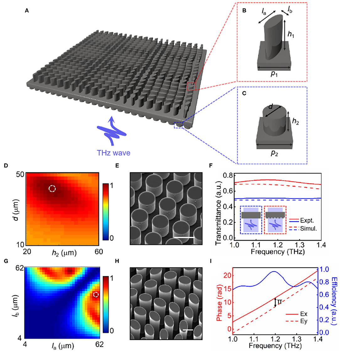
Figure 1. Geometric designs and THz properties of the antireflection-layer-integrated metasurface. Schematic illustrations of (A) metasurface, (B) elliptical, and (C) circular silicon pillars, respectively. (D) Dependency of transmittance on d and h2 at 1.20 THz. (E) SEM image of circular silicon pillars. (F) Frequency dependent transmittances of metasurfaces with (red) and without (blue) the antireflection layer. The insets show the corresponding metasurfaces. (G) Dependency of circular polarization conversion ratio on la and lb at 1.20 THz. (H) SEM image of elliptical silicon pillars. (I) Frequency dependent resonant phase of the pillar with la = 60 μm and lb = 40 μm under x- (red solid) and y- (red dot) incident polarizations and corresponding circular polarization conversion ratio (blue solid). All scale bars indicate 50 μm.
Elliptical pillars are spatially arranged on the other side to introduce the desired PB phase (Figure 1B). The phase retardation of each anisotropic unit can be calculated by Jones matrix as:
where α is the orientation angle, I is the identity matrix, R is the rotation matrix, ζ = πδnd/λ is half of the phase retardation, δn, d and λ are unit birefringence, height and incident wavelength, respectively. The latter term in Equation (1) can be ignored at half-wave condition. For circular polarization incidences Ein = χ(±) = (1, ±i)T/21/2, where + for left circular polarization (LCP) and—for right circular polarization (RCP), the output wave is depicted as:
After passing through such a meta-unit, LCP is converted to RCP and the wave is encoded with a phase of exp(i2α). The 0°–180° rotation of the meta-unit induces a full phase modulation. Meanwhile, RCP is converted to LCP and a conjugated phase is encoded.
We optimize the geometry of elliptical pillars to reach the half-wave condition. The refractive index of intrinsic silicon at 1.20 THz is 3.45. We fix p1 = 70 μm, h1 = 275 μm and change the major axis la and minor axis lb of the elliptical pillar in the range of 4–62 μm, separately. The obtained circular polarization conversion ratio (CPCR) is recorded (Figure 1G). We select la = 60 μm and lb = 40 μm to achieve the maximum CPCR. Figure 1H reveals the metasurface composed of elliptical silicon pillars with uniform geometries and different orientations. Figure 1I presents the simulated phases for Ex and Ey incidences and corresponding CPCR, respectively. The phase increases linearly with frequency due to the high-order waveguide resonances excited inside the dielectric pillars. The phase retardation reaches almost π at 1.20 THz, and a maximum CPCR of 97% is obtained accordingly. The deviation from 1.20 THz leads to a reduction of CPCR.
A standard photolithography and reactive ion etching process are carried out on a 1,000-μm-thick double-polished intrinsic silicon wafer to fabricate both circular and elliptical pillars. The wafer is ultrasonically bathed and O-plasma treated (IoN Wave 10, PVA-TePla, USA). A photoresist (AZ4620, Clariant GmbH, Germany) layer is spin-coated onto the cleaned wafer at 3,000 rpm for 45 s and then baked for 10 min at 95°C. The desired pattern is carried out via photolithography process (MJB4, Suss MicroTec Lithography GmbH, Germany). Subsequently, the exposed sample is developed and baked for 1 min at 115°C. Reactive ion etching (HSE200, NAURA Technology Group Co., China) is conducted cyclically, and each cycle includes a 2 s vacuum for removing residual gas, 1 s SF6 etching and 3 s C4F8 passivating. After etching, the residual photoresist is lifted off by acetone. To increase the yield, the thinner antireflection layer is fabricated first and then the elliptical pillars are fabricated in a similar process. Then the sample is observed with a scanning electron microscope (SEM, Quanta200, TSS Microscopy, USA) to check the geometric parameters. Simulations are performed with a commercial software Lumerical FDTD Solutions. Transmissions are characterized with a THz time-domain spectroscopy (THz-TDS, TAS7400SP, Advantest Corporation, Japan).
Results
Via rationally designing the spatial orientation of meta-units, the wavefront of THz beam could be freely manipulated. First, an antireflection-layer-integrated metalens is demonstrated, which is a commonly used element in THz imaging and communications. The phase profile of a lens (Figure 2A) is depicted as [30, 31]:
where f is the focal length and (x, y) is the position coordinate. Here, f is set as 8 mm. The photograph of fabricated sample (Figure 2B) vividly shows a morphology consistent with the phase diagram. A scanning near-field THz microscope (SNTM, TP800, Terahertz Photonics Co. Ltd., China) is utilized to characterize the performance of the metalens. Figure 2C exhibits the intensity distributions before and after focusing, and a lateral image of the focusing process. It verifies the excellent focusing performance of fabricated metalens. Figure 2D shows the intensity profiles of incident wave and focal spot, respectively. The full wave at half maximum (FWHM) at the focal plane is 1.48λ = 370 μm, which is close to the theoretical diffraction limit λ/2NA = 235 μm. The measured focusing efficiency, which is defined as the intensity at the focal plane divided by total incident power, is shown in Figure 2E. It slightly deviates from the simulation, and the maximum efficiency of 95% is obtained at 1.10 THz, which is attributed to the imperfect manufacturing.
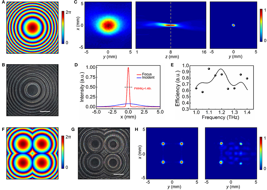
Figure 2. Metalens and metalens array. (A) Designed phase diagram and (B) photograph of a metalens. (C) THz intensity distributions of incident wave in the xy-plane (left), beam propagation in the xz-plane (middle), and focal spot in the xy-plane (right). (D) Intensity profiles of incident wave (blue) and focal spot (red). (E) Simulated (line) and measured (dot) efficiencies of the metalens. (F) Designed phase diagram and (G) photograph of a metalens array. (H) Simulated (left) and measured (right) intensity distributions in the focal plane. All scale bars indicate 2 mm.
Lens array shows superiority in multi-pixel imaging [32, 33] and multi-parameter detection [34], and is a key element in THz cameras and communication systems. Here, we fabricate a 2 × 2 metalens array with an optimized phase distribution to match the size of THz wave spot (Figure 2F). The fabricated metalens array with f = 7 mm is presented in Figure 2G. With a Gaussian incidence, measured focal points are consistent with the simulation (Figure 2H). The efficiency reaches 81% at 1.15 THz, indicating an excellent antireflection performance.
Polarization fork grating can encode a designed orbital angular momentum (OAM) to diffraction orders. Such beams play important roles in mode division multiplexing communication [35] and multi-photon quantum computing [36]. The phase of a polarization fork grating is expressed as:
where θ is the deflection angle, and m denotes the topological charge. Here, a polarization fork grating with θ = 15° and m = 1 at 1.20 THz is fabricated. Its theoretical phase diagram is shown in Figure 3A. The fabricated sample is coincident with the diagram (Figure 3B). For linear polarized incidence, the wave is deflected to two diffraction orders and forms two vortices (Figures 3C,D). The measured phase distribution indicates m of two generated vortices are ± 1, respectively (Figure 3E). The residual energy at 0th order is due to the small coverage of incident wave on the sample. The measured transmittance of the polarization fork grating is 81% at 1.10 THz.
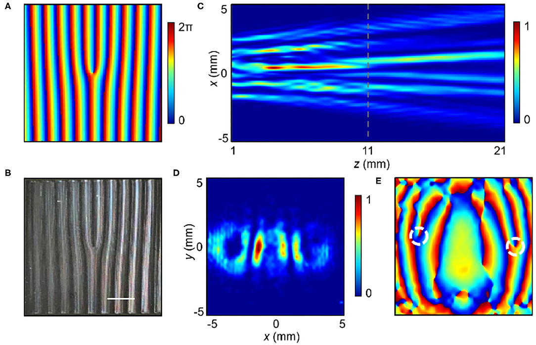
Figure 3. Polarization fork grating. (A) Phase profile and (B) photograph of a polarization fork grating. The scale bar indicates 2 mm. Measured intensity distributions in the (C) xz-plane and (D) xy-plane at z = 11 mm. (E) Measured phase distribution at z = 11 mm.
High-order Bessel beam is a Bessel beam carrying OAM, which exhibits unique non-diffractive vortex, making it useful in wireless communications [37] and micro-manipulations [38, 39]. It can be generated by a spiral axicon, the phase of which is depicted as:
where θ is the radial deflection angle. Here, the designed θ is 15° at 1.20 THz and m = 1. The phase diagram and photograph of the spiral axicon are shown in Figure 4A. The far-field phase diagram of generated Bessel vortex reveals a spiral distribution (Figure 4B). The simulated and measured intensity distributions match very well (Figure 4C). For LCP incidence, the intensity distribution in the xy-plane is a series of concentric rings with exponentially decayed intensity. Its non-diffraction property is verified in a focal depth of 8 mm. The measured efficiency reaches 68% at 1.30 THz.
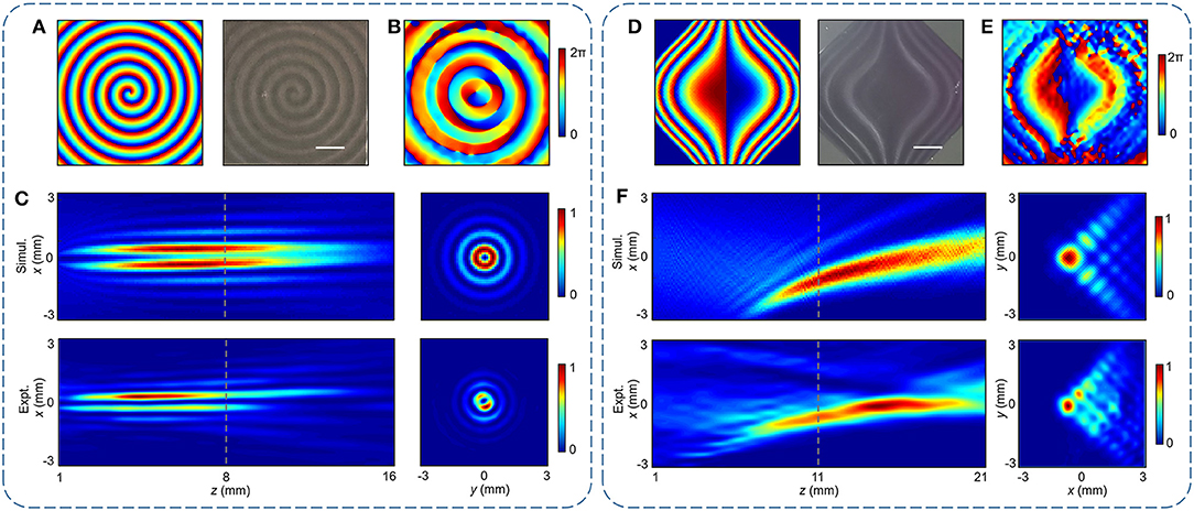
Figure 4. Spiral axicon and polarization Airy mask. (A) Phase diagram and photograph of a Bessel vortex generator. (B) Far-field phase diagram of the generated Bessel vortex beam. (C) Simulated and measured intensity distributions of the generated Bessel vortex beam in the xz- and xy-planes. (D) Phase diagram and photograph of a polarization Airy mask. (E) Far-field phase diagram of the generated Airy beam. (F) Simulated and measured intensity distributions of the generated Airy beam in the xz- and xy-planes. All scale bars indicate 2 mm.
Airy beam is another kind of specific beam with great potentials in particle manipulation [40] and light-sheet microscopy [41]. It exhibits unique properties such as non-diffraction, transverse acceleration and self-healing. The phase of a 2D Airy mask is expressed as:
where a = 2 × 10⁻¹⁰ is a positive parameter. The phase diagram and photograph of the polarization Airy mask are shown in Figure 4D. The far-field phase diagram of generated Airy beam is presented in Figure 4E. The simulated and measured intensity distributions match very well (Figure 4F). For LCP incidence, the main lobe of Airy beam with small curvature appears at 6 mm behind the sample, and a series of side lobes coexist with the main lobe. The xy-plane image at z = 11 mm vividly reveals the THz intensity distribution of the generated Airy beam. The measured transmittance reaches 95% at 1.10 THz.
Discussion
The bi-layer design, which consists of micro-pillar arrays on both sides of the wafer, is conducted in a same micro-fabrication process on the same silicon wafer. It provides a practical strategy for arbitrary THz phase modulation with merits of compactness and high efficiency. The antireflection performance for the target frequency can be optimized via properly designing the geometry. PB phase modulation is accomplished by spatially arranging the orientations of inhomogeneous dielectric pillars. The subwavelength meta-unit enables high resolution and pronounced flexibility of wavefront control. The efficiency of these metadevices can be improved via optimizing the half-wave condition at the target frequency. With the combination of two micro-pillar arrays with distinguishing functions on both sides, a compact method for high-efficiency metadevices available for arbitrary THz beam shaping is proposed.
Conclusion
In summary, we propose an integrated antireflection strategy for transmissive THz metadevices. Different THz PB phase metadevices including metalens, metalens array, polarization fork grating, spiral axicon and polarization Airy mask are demonstrated. With an optimized circular-pillar antireflection layer, the reflection loss of above metadevices are significantly suppressed. High efficiency and excellent design flexibility of this strategy are verified. It provides a practical platform for planar THz elements which suit for high-performance THz imaging and communication.
Data Availability Statement
The original contributions presented in the study are included in the article/supplementary material, further inquiries can be directed to the corresponding author/s.
Author Contributions
WH conceived the original idea, designed the experiment, supervised, and directed the research. XL and ZS prepared the samples and performed the experiments. XL, ZS, QT, and WH analyzed the experimental data. XL, ZS and WH prepared the initial manuscript. All authors participated in the discussion and contributed to refining the manuscript.
Funding
This work was supported by the National Natural Science Foundation of China (NSFC) (62035008 and 61922038), National Key Laboratory Foundation (6142411195411).
Conflict of Interest
The authors declare that the research was conducted in the absence of any commercial or financial relationships that could be construed as a potential conflict of interest.
References
1. Zhang XC, Xu J. Introduction to THz Wave Photonics. New York, NY: Springer (2010). doi: 10.1007/978-1-4419-0978-7
2. Kleine-Ostmann T, Nagatsuma T. A review on terahertz communications research. J Infrared Millim Terahertz Waves. (2011) 32:143–71. doi: 10.1007/s10762-010-9758-1
3. Song HJ, Nagatsuma T. Present and future of terahertz communications. IEEE Trans Terahertz Sci Technol. (2011) 1:256–63. doi: 10.1109/TTHZ.2011.2159552
4. Koenig S, Lopez-Diaz D, Antes J, Boes F, Henneberger R, Leuther A, et al. Wireless sub-THz communication system with high data rate. Nat Photonics. (2013) 7:977–81. doi: 10.1038/nphoton.2013.275
5. Ferguson B, Zhang XC. Materials for terahertz science and technology. Nat Mater. (2002) 1:26–33. doi: 10.1038/nmat708
6. Masson JB, Gallot G. Terahertz achromatic quarter-wave plate. Opt Lett. (2006) 31:265–7. doi: 10.1364/OL.31.000265
7. Yu N, Genevet P, Kats MA, Aieta F, Tetienne JP, Capasso F, et al. Light propagation with phase discontinuities: generalized laws of reflection and refraction. Science. (2011) 334:333–7. doi: 10.1126/science.1210713
8. Yu N, Capasso F. Flat optics with designer metasurfaces. Nat Mater. (2014) 13:139–50. doi: 10.1038/nmat3839
9. Meinzer N, Barnes WL, Hooper IR. Plasmonic meta-atoms and metasurfaces. Nat Photonics. (2014) 8:889–98. doi: 10.1038/nphoton.2014.247
10. Arbabi A, Horie Y, Bagheri M, Faraon A. Dielectric metasurfaces for complete control of phase and polarization with subwavelength spatial resolution and high transmission. Nat Nanotechnol. (2015) 10:937–43. doi: 10.1038/nnano.2015.186
11. Singh R, Cao W, Al-Naib I, Cong L, Withayachumnankul W, Zhang W. Ultrasensitive terahertz sensing with high-Q Fano resonances in metasurfaces. Appl Phys Lett. (2014) 105:171101. doi: 10.1063/1.4895595
12. Ghasemi M, Choudhury P. Nanostructured concentric gold ring resonator-based metasurface filter device. Optik. (2016) 127:9932–6. doi: 10.1016/j.ijleo.2016.07.048
13. Liu X, Fan K, Shadrivov IV, Padilla WJ. Experimental realization of a terahertz all-dielectric metasurface absorber. Opt Express. (2017) 25:191–201. doi: 10.1364/OE.25.000191
14. Zhou S, Shen Z, Kang R, Ge S, Hu W. Liquid crystal tunable dielectric metamaterial absorber in the terahertz range. Appl Sci. (2018) 8:2211. doi: 10.3390/app8112211
15. Lee WSL, Nirantar S, Headland D, Bhaskaran M, Sriram S, Fumeaux C, et al. Broadband terahertz circular-polarization beam splitter. Adv Opt Mater. (2018) 6:852. doi: 10.1002/adom.201700852
16. Yoon G, Lee D, Nam KT, Rho J. Geometric metasurface enabling polarization independent beam splitting. Sci Rep. (2018) 8:9468. doi: 10.1038/s41598-018-27876-2
17. Liu S, Cheng Q, Xu Q, Wang TQ, Du LL, Luan K, et al. Free-standing metasurfaces for high-efficiency transmitarrays for controlling terahertz waves. Adv Opt Mater. (2016) 4:384–90. doi: 10.1002/adom.201500519
18. Jia M, Wang Z, Li H, Wang X, Luo W, Sun S, et al. Efficient manipulations of circularly polarized terahertz waves with transmissive metasurfaces. Light Sci Appl. (2019) 8:16. doi: 10.1038/s41377-019-0127-0
19. Chang CC, Headland D, Abbott D, Withayachumnankul W, Chen HT. Demonstration of a highly efficient terahertz flat lens employing tri-layer metasurfaces. Opt Lett. (2017) 42:1867–70. doi: 10.1364/OL.42.001867
20. Akram MR, Mehmood MQ, Bai X, Jin R, Premaratne M, Zhu W. High efficiency ultrathin transmissive metasurfaces. Adv Opt Mater. (2019) 7:1801628. doi: 10.1002/adom.201801628
21. Akram MR, Bai X, Jin R, Vandenbosch GAE, Premaratne M, Zhu W. Photon spin hall effect-based ultra-thin transmissive metasurface for efficient generation of OAM waves. IEEE Trans Antennas Propag. (2019) 67:4650–8. doi: 10.1109/TAP.2019.2905777
22. Zhang H, Zhang X, Xu Q, Wang Q, Xu Y, Wei M, et al. Polarization-independent all-silicon dielectric metasurfaces in the terahertz regime. Photonics Res. (2017) 6:24. doi: 10.1364/PRJ.6.000024
23. Khorasaninejad M, Chen WT, Devlin RC, Oh J, Zhu AY, Capasso F. Metalenses at visible wavelengths: diffraction-limited focusing and subwavelength resolution imaging. Science. (2016) 352:1190–4. doi: 10.1126/science.aaf6644
24. Zhou Y, Xu X, Hu F, Zheng X, Li W, Zhao P, et al. Graphene as broadband terahertz antireflection coating. Appl Phys Lett. (2014) 104:051106. doi: 10.1063/1.4863838
25. Zhang B, Hendrickson J, Nader N, Chen H-T, Guo J. Metasurface optical antireflection coating. Appl Phys Lett. (2014) 105:241113. doi: 10.1063/1.4904827
26. Kröll J, Darmo J, Unterrainer K. Metallic wave-impedance matching layers for broadband terahertz optical systems. Opt Express. (2007) 15:6552–60. doi: 10.1364/OE.15.006552
27. Zi J, Xu Q, Wang Q, Tian C, Li Y, Zhang X, et al. Antireflection-assisted all-dielectric terahertz metamaterial polarization converter. Appl Phys Lett. (2018) 113:101104. doi: 10.1063/1.5042784
28. Arbabi A, Horie Y, Ball AJ, Bagheri M, Faraon A. Subwavelength-thick lenses with high numerical apertures and large efficiency based on high-contrast transmitarrays. Nat Commun. (2015) 6:7069. doi: 10.1038/ncomms8069
29. Born M, Wolf E. Principles of Optics, 7th (expanded) ed. London: Press Syndicate of the University of Cambridge. (1999). p. 461.
30. Shen Z, Zhou S, Li X, Ge S, Chen P, Hu W, et al. Liquid crystal integrated metalens with tunable chromatic aberration. Adv Photonics. (2020) 2:036002. doi: 10.1117/1.AP.2.3.036002
31. Zhou S, Shen Z, Li X, Ge S, Lu Y, Hu W. Liquid crystal integrated metalens with dynamic focusing property. Opt Lett. (2020) 45:4324–7. doi: 10.1364/OL.398601
32. Fan ZB, Qiu HY, Zhang HL, Pang XN, Zhou LD, Liu L, et al. A broadband achromatic metalens array for integral imaging in the visible. Light Sci Appl. (2019) 8:67. doi: 10.1038/s41377-019-0178-2
33. Lin RJ, Su VC, Wang S, Chen MK, Chung TL, Chen YH, et al. Achromatic metalens array for full-colour light-field imaging. Nat Nanotechnol. (2019) 14:227–31. doi: 10.1038/s41565-018-0347-0
34. Zhao M, Yang Z, Yuan X, editors. All-dielectric metalens array for optical multi-parameters detection. In: Yuan X, editors. Imaging Systems and Applications. Optical Society of America (2019). doi: 10.1364/ISA.2019.IM2B.3
35. Zhang W, Zheng S, Hui X, Dong R, Jin X, Chi H, et al. Mode division multiplexing communication using microwave orbital angular momentum: an experimental study. IEEE Trans Wirel Commun. (2017) 16:1308–18. doi: 10.1109/TWC.2016.2645199
36. Hiesmayr B, De Dood M, Löffler W. Observation of four-photon orbital angular momentum entanglement. Phys Rev Lett. (2016) 116:073601. doi: 10.1103/PhysRevLett.116.073601
37. Heebl JD, Ettorre M, Grbic A. Wireless links in the radiative near field via Bessel beams. Phys Rev Appl. (2016) 6:034018. doi: 10.1103/PhysRevApplied.6.034018
38. Arlt J, Garcés-Chávez V, Sibbett W, Dholakia K. Optical micromanipulation using a Bessel light beam. Opt Commun. (2001) 197:239–45. doi: 10.1016/S0030-4018(01)01479-1
39. McGloin D, Garcés-Chávez V, Dholakia K. Interfering Bessel beams for optical micromanipulation. Opt Lett. (2003) 28:657–9. doi: 10.1364/OL.28.000657
40. Baumgartl J, Mazilu M, Dholakia K. Optically mediated particle clearing using Airy wavepackets. Nat Photonics. (2008) 2:675–8. doi: 10.1038/nphoton.2008.201
Keywords: terahertz, beam shaping, metadevice, specific optical field, antireflection
Citation: Li X, Shen Z, Tan Q and Hu W (2021) High Efficient Metadevices for Terahertz Beam Shaping. Front. Phys. 9:659747. doi: 10.3389/fphy.2021.659747
Received: 28 January 2021; Accepted: 05 March 2021;
Published: 26 March 2021.
Edited by:
Shaohua Tao, Central South University, ChinaReviewed by:
Weiren Zhu, Shanghai Jiao Tong University, ChinaKapil Debnath, Indian Institute of Technology Kharagpur, India
Copyright © 2021 Li, Shen, Tan and Hu. This is an open-access article distributed under the terms of the Creative Commons Attribution License (CC BY). The use, distribution or reproduction in other forums is permitted, provided the original author(s) and the copyright owner(s) are credited and that the original publication in this journal is cited, in accordance with accepted academic practice. No use, distribution or reproduction is permitted which does not comply with these terms.
*Correspondence: Wei Hu, aHV3ZWlAbmp1LmVkdS5jbg==