 Tzveta Apostolova
 Vasyl Kurylo3
- 1Institute for Nuclear Research and Nuclear Energy, Bulgarian Academy of Sciences, Sofia, Bulgaria
- 2Institute for Advanced Physical Studies, New Bulgarian University, Sofia, Bulgaria
- 3NoviNano Lab LLC, Lviv, Ukraine
- 4Department of Photonics, Lviv Polytechnic National University, Lviv, Ukraine
Diamond laser engineering is of great importance for designing devices, which find applications in radiation sensing and quantum technologies. A review of the present state of the art of experimental and theoretical studies on ultrashort laser irradiation of diamond is presented. For a wide range of laser parameters, the optimization of laser-induced electronic, optical and structural modifications of diamond requires quantitative understanding of the microscopic processes underlying the high electronic excitation in the material.
1 Introduction
Diamond is an indirect wide band gap semiconductor which has numerous exceptional material parameters like extreme hardness and thermal conductivity not matched by any solid [1, 2], high electric breakdown field, high electron and hole mobilities [3], high carrier saturation rate, possible implementation of several color centers with applications in quantum technologies [4, 5] and high biocompatibility. The speed of sound propagation in diamond is also high. Some basic characteristics of diamond are summarized in Table 1.
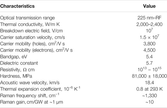
TABLE 1. Basic characteristics of diamonds.
Diamond has extraordinary optical characteristics. It is transparent in the ultraviolet, visible, infrared and microwave spectral regions. The absorption coefficient of diamond depends on the laser wavelength and on the properties of the carbon material as shown in Figure 1 [6]. Some crystals are almost transparent to laser light, while others strongly absorb it. Due to the high refractive index in the visible and ultraviolet ranges, diamond is a useful material for dielectric [7] and hybrid nanophotonic devices [8–10]. When irradiated with intense ultrashort laser pulses diamond can be converted into a short-lived plasmonic state enabling the photoexcitation and the propagation of surface plasmon-polaritons (SPPs). Possible applications are spatial phase modulation, high-speed optical switching and saturable absorption [11, 12]. The availability of advanced technologies for the production of pure single-crystal diamond [13, 14] allows to study the formation of electron–hole liquid (EHL) [15, 16] in the material which can help to reveal the mechanisms of phase transitions occuring in a strongly excited diamond. These technologies have also allowed the formation of atomically flat diamond (111) surfaces that can subsequently undergo graphitization [17].
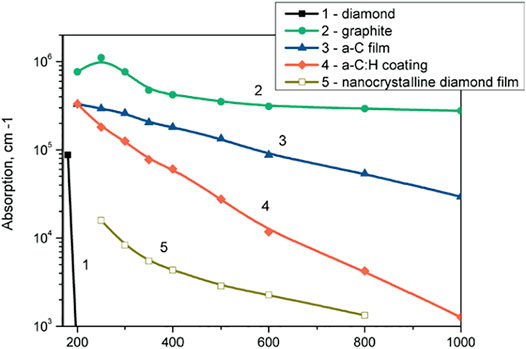
FIGURE 1. Dependence of the optical absorption coefficient on the laser wavelength [6].
Currently, diamond can be obtained not only in the form of natural monocrystals. Technologies have been developed that provide the opportunity to grow synthetic diamonds with parameters and properties similar or even better than those of natural crystals. There are several ways to obtain diamond crystals. The oldest one is based on high-pressure high-temperature (HPHT) compression of a high purity carbon source into a metal solvent [18]. This allows growing a single or polycrystalline diamond, generally with inclusions of impurities, mainly nitrogen that degrades the electrical and optical properties of the material. The method to obtain the purest material [19] uses chemical vapor deposition (CVD) of diamond from different gas mixtures, mainly hydrogen with a percentage of hydrocarbons and possibly oxygen. The size of such crystals is much larger than the size of the crystals obtained from HPHT synthesis and their thickness varies from a few nanometers to several centimeters. Homoepitaxial growth can also be feasible with the CVD method. Synthetic diamond possesses the properties of the purest natural diamond. For instance, homoepitaxial tissue-equivalent CVD diamond has substituted for natural diamond as a base material for dosimeters used in radiotherapy [20]. Homoepitaxially grown monocrystalline diamond is fabricated with a maximum size of about 1 cm2 due to the availability of diamond substrates and its application is limited. Although comparatively large area monocrystalline samples are obtained via heteroepitaxial growth, their electronic quality is still a subject of intense investigation [21]. Diamond materials can vary greatly in characteristics according to the inclusions of impurities and structural defects. In comparison to the traditional techniques for laser processing intense ultrashort laser pulses interact with diamond non-linearly, minimizing thermal diffusion and providing low ablation threshold, reduced thickness of graphite layer on the ablated surface and high spatial resolution beyond the diffraction limit [22–24]. Precise femtosecond laser profiling of diamond crystals resulted in fabrication of X-ray refractive lenses [25]. The technology of laser induced periodic surface structures (LIPSS) [26] is also developing successfully. Thanks to it, there has been an attempt to create high-quality anti-reflective surfaces on diamond with Raman lasers [27]. Laser processing is also used to create a variety of microstructures inside the bulk of diamond. Due to the movement of the focus of the laser beam through the crystal, it is possible to make structures of different shapes and sizes [28–30]. 3D architecture has been proposed for radiation hard detectors with timing capabilities and for dosimeters with high spatial resolution applied in radiotherapy. This involves fabricating columnar electrodes in the diamond bulk by laser irradiation [31]. New high-quality methods of processing diamond will open the way for using this material in new industries.
2 Diamond Surface Treatment
Pulsed laser processing of the surface of diamond can result into a complete conversion of diamond to monocrystalline graphite as demonstrated by Raman spectroscopy [32]. Since the absorption coefficient of graphitic materials is higher than that of different forms of diamond in a broad spectral range, the decrease of optical transmittance serves as an experimental indication of surface graphitization of diamond [6, 33]. Figure 2 shows the change in the transmittance of CVD polycrystalline diamond as a function of the number of irradiating picosecond pulses for varying laser fluence. For the highest fluence the decrease of transmittance starts from the first irradiating pulse while the number of pulses required to induce surface graphitization increases with decrease of laser fluence. Raman spectroscopy showed that surface ablation of polycrystalline diamond occurred without significant graphitization when femtosecond laser pulses were used [34]. In [35] LIPSS were formed on CVD mono-crystalline diamond surface perpendicular to the direction of laser polarization with spatial periods 125 and 400 nm corresponding to femtosecond laser irradiation with wavelengths λ = 248 and λ = 800 nm, respectively. Wires of millimeter length composed of 150 nm ripples (high spatial frequency–HSF LIPSS) perpendicular to the direction of laser polarization were obtained after irradiation of synthetic single-crystal diamond with near-infrared femtosecond laser pulses with fluences close to the ablation threshold [36]. Three types of LIPSS were formed after irradiation with femtosecond laser pulses in the visible and near infrared spectral range–first one with subwavelength periodicity, the second one with spacial period ∼λ/3 and the third one with a spatial period close to the laser wavelength (low spatial frequency LSFL LIPSS) [37]. It was also found that the spatial periods of HSF LIPSS increase from 170 to 190 nm when laser fluence increases 1.5 times [38]. The experimental results showed that the spatial periods of LIPSS depend on the wavelength of the laser, the polarization of the laser electric field, the number of pulses and the laser fluence.
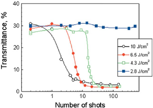
FIGURE 2. Transmission properties of the CVD diamond sample with varying fluence and number of laser pulses [30].
High quality diamond nano-structures with surface roughness below 1.4 nm were produced by using a Ti: Sapphire laser pulses of 130 fs at a repetition rate of 1 kHz at a central wavelength of 800 nm. Surface structures in the 100–400 nm range [27] were produced for λ = 400 nm. The ablation threshold was 2 J/cm2, which corresponds to previous studies in which 100 fs pulses were used with λ = 400 nm [39]. Figure 3A shows the values of laser fluence and scanning speed used for the fabrication of low-roughness LSF LIPSS with period of ∼400 nm. The high quality LSF structures shown in Figure 3B were formed at the irradiated location on the diamond surface for fluences ranging from 2 to 6 J/cm2 and scanning speeds from 100 to 300 μm/s. Figure 3C shows a lineout of the structures along the x-axis obtained by AFM measurements. When there are deviations from the obtained set of parameters, the optical quality of structures is reduced. At energies exceeding 6 J/cm2, intense ablation occurs. As a result, HSF structures predominate in the treated areas. It was demonstrated that when high number of laser pulses and low laser fluence were used HSF ripples were predominantly formed [40], while LSF structures were obtained when the number of pulses was low and the fluence was high. It was found that the difference in the threshold fluences for the formation of the two types of ripples was 5.4 J/cm2. In [41] 200 fs laser pulses with wavelength 515 nm were used to obtain coarse and fine ripples on monocrystalline diamond surface. Figures 4A–C show the ablative craters produced on the surface and the formation of LSF (coarse CR) and HSF (fine FR) LIPSS structures with a period ∼ 100 nm, staring for number of laser pulses N > 3,4. For N > 10 the shallow FR and CR ripples become very pronounced (Figure 4B). Coarse ripples disappear for N > 100 at the laser modified spot center due to ablation as seen in Figure 4D. Both LSFL and HSFL were oriented perpendicularly to laser polarization within the ablation crater. The dependence of HSF and LSF LIPSS on the number of pulses N was also obtained (Figure 5). Studies of the optical characteristics of laser-treated diamonds were performed. The laser setup used is based on Spectra-Physics Tsunami S with wavelength 800 nm, peak power >0.7 W, pulse duration 100 fs and repetition rate 80 MHz. The formation of LIPSS oriented perpendicular to the direction of polarization took place using a laser beam with a fluence of 20 J/cm2 [42]. Structures were formed with a ripple period in the range of 170 ± 10 nm with structure length greater than 5 μm. In Figure 6A Raman spectra of CVD diamond samples before and after the laser treatment are shown. In the inset, a clearly defined diamond peak for the untreated sample (black line) is shown at 1,332.2 cm−1, typical of diamond [43]; the treated sample (red line) shows a shift of the peak to 1,333.1 cm−1. This is interpreted as an indication of compressive stress caused by laser irradiation. No peak is exhibited at 1,560 cm−1 indicating absence of graphitic phase. In Figure 6B the transmitance of laser irradiated polycrystalline diamond sample in comparison to an untreated diamond sample is shown. Since laser irradiation induces defect states in the sample, the transmission of diamond decreases by more than 80% in the visible range (from 32 to 4.5% for 500 nm) and by 70% in the IR range (from 50.2 to 11.7 for 1,500 nm).
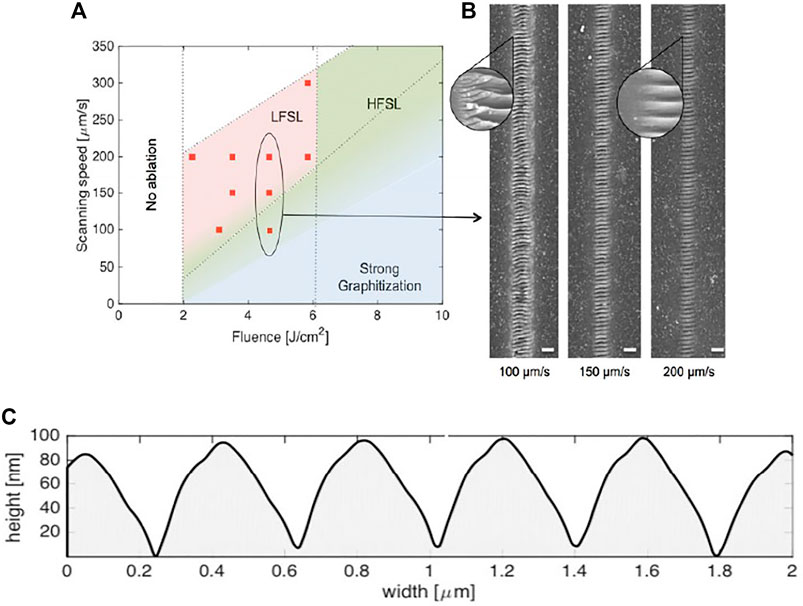
FIGURE 3. (A) Formation of diamond structures depending on laser fluence and scanning speed. (B) Morphology of the nano-ripples for different scanning speeds at a fixed fluence. Scale bar = 1 μm. (C) Line-out of the surface structures [27].
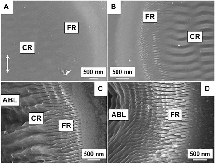
FIGURE 4. SEM images of ablation crater edge (ABL), fine (FR) and coarse (CR) ripples formed within the craters on diamond surface for different number of pulses: 10 (A), 30 (B), 100 (C), and 300 (D) [41].
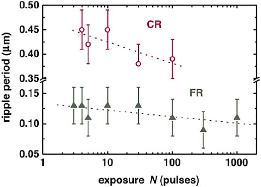
FIGURE 5. Pulse number-dependence of the variation of CR and FR periods. The dotted lines represent qualitatively the cumulative trends [41].
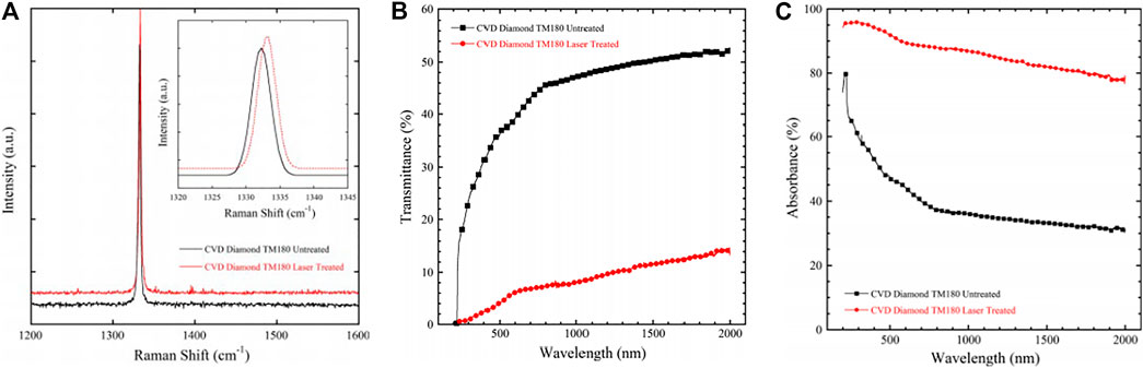
FIGURE 6. Comparison of Raman spectra (A), transmittance spectra (B), absorbance spectra (C) of CVD diamond before and after fs-laser treatment [42].
After laser treatment, the absorbance of the polycrystalline diamond sample increases in the entire wavelength range under consideration. For the visible and IR wavelengths it increases up to 80% as seen in Figure 6C. In the UV range (close to the value of diamond indirect bandgap of 5.47 eV) the absorbance is close to 95%. Femtosecond laser treatment leads to the appearance of surface defect states in the band gap of diamond, which can act as traps or recombination centers [29, 44–46].
3 Diamond Bulk Treatment
Besides the surface treatment of diamond crystals, it is also possible to process the bulk of the material [29, 47, 48]. Three-dimensional conductive microstructures at any depth inside bulk diamond [30] and of arbitrary shape can be created by translating the sample through the focus of the laser pulse. Raman microspectroscopy showed that the laser modified material is a mixture of amorphous and graphitic sp2 bonded carbon with sp3 bonded diamond [30, 49]. A strong correlation between the conductivity of the obtained structures and their graphitic content was also evidenced [32]. The complete laser-induced phase transformation of diamond bulk into sp2 carbon is hindered by the fact that it produces both compressive and tensile stresses due to substantial difference in densities of two carbon allotropes. As a result the conductive structures usually consists of a large number of micro-and nano-inclusions of sp2-carbon in sp3 diamond matrix and the conductivity of the laser-treated area is likely to be controlled by a percolation mechanism [32]. A novel technique demonstrated laser induced controlled generation of layered extended defects in diamond. To study the structural morphology of a single-crystal diamond, a titanium-sapphire laser was used, generating 140 fs pulses at a wavelength of 800 nm with a repetition rate of 1 kHz. Figure 7A [50] shows how the sample mounted on the XYZ translation table was scanned at a raster speed of 50 μm/s along the Y axis with a simultaneous slow movement 0.6 μm/s along the Z axis away from the laser. As a result, an opaque “plate” of thickness ∼8 μm was fabricated inside the diamond sample. After processing, SEM microscopy of the polished surface (110) of the sample (Figure 7B) showed numerous transparent spots of irregular shape distributed in the XZ plane of the laser-modified region. It was found that their number and size depend on the processing conditions and their occurrence was due to the predominant graphitization along the cracks formed in diamond in the path of the laser beam. Cracks were most likely to occur along the {111} planes [50, 51]. Scanning Spreading Resistance Microscopy (SSRM) revealed that the nanocracks had higher conductivity with respect to the main modified path. Based on this observation it was concluded that the graphitization processes was mainly localized inside the nanocracks forming thin graphitic-carbon sheets while the gaps between them were filled by diamond. The state-of-the-art experimental research has achieved the fabrication of electrically conductive paths along multiple nano-scale poorly connected sp2-bonded graphitic columns and a network of strain-relieving micro-cracks [52]. The control of the modified material conductivity is of paramount importance for technological applications.
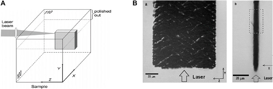
FIGURE 7. (A) Microstructuring of diamond bulk with femtosecond laser pulses, (B) transmission optical micrographs of side view of the modified region [50].
The design of optical wave-guides in the bulk of a diamond crystal is also investigated based on the principles of diamond bulk graphitization. The obtained electrically conductive graphitized phase has been successfully used to fabricate radiation detectors [53]. Due to the lower density of the sp2 phase as compared to the density of the sp³ phase, a strong localized stress field is created in the surrounding pure diamond, which could act as an optical waveguide. In Type II waveguide, the optical mode confinement was achieved between two closely spaced and parallel laser-inscribed conducting wires. The scheme of fabrication of the waveguide is shown in Figure 8 [54]. The type II waveguides have high polarization dependence permitting strong transmission for vertically polarized light while the transmission for the horizontal polarization state of light is negligible. Waveguides were fabricated using a 790 nm wavelength laser pulse of duration 100 fs and a repetition rate of 1 kHz. By improving and complicating the design of the waveguide, a Y splitter can be obtained from the Type II waveguides as shown in Figure 9A [55]. At the entrance, there is a single type II waveguide and at a distance of 1 mm, it is divided into two. As a result, two waveguides are formed separated by 20 μm. The outputs coupling ratio can be varied by translating the input fiber along the z-axis. A splitting ratio of 50:50 is seen in the near field mode image (Figure 9D). In this case, the overall transmission of the structure is 7 dB, which corresponds to a propagation loss of 18 dB/cm. For the manufacture of Type III waveguides that support both polarization modes, it is possible to form tubular structures, as shown in Figure 10 [55]. The radius of such structures is 10 μm. Laser-written 32 graphite tracks are arranged in a circular manner with a center-to-center spacing 2 μm between each two tracks. The waveguides had an insertion loss of 5.5 dB for the vertical polarization mode and 11.5 dB for the horizontal polarization mode. Type III waveguides were multimode for both polarizations, with minimal losses. Such structures cannot be fabricated without the use of adaptive optics. Due to the symmetrical structure of the Type III waveguide, it is insensitive to polarization. Due to the asymmetry of the graphite tracks as well as the asymmetry of the laser focus, a difference in transmission is formed for vertical and horizontal polarization. The sides of the waveguide are continuous, and the bottom and top contain unmodified sections that separate the graphite tracks. The ability to manufacture waveguides in the bulk of the material and integrate them into optical fiber systems is a promising topic. However, propagation losses are relatively high compared with optical nanocavities obtained by plasma etching [56]. It is nevertheless apparent that the plasma shaping of microstructures in diamond requires a complex process of masking and plasma etching on the surface of a sample. Laser writing of waveguides in the diamond bulk is on the contrary a real time process and the graphitization of the material can follow arbitrary paths inside the diamond bulk. This can result in a new technology of programmable laser shaping of a number of optoelecronic devices, once the properties of the modified material are properly understood and controlled.
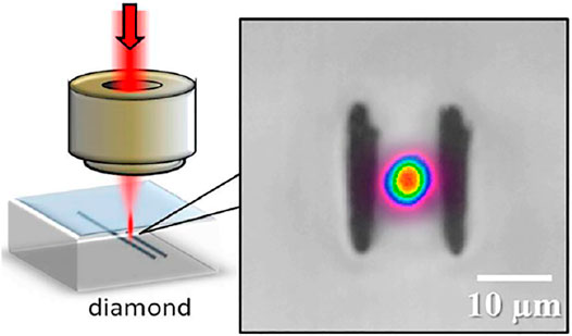
FIGURE 8. Type II waveguide geometry and transverse view optical microscope image of type II modification in diamond. Creative Commons Attribution License [54].
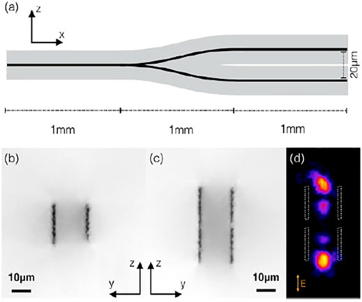
FIGURE 9. (A) Schematic view of the vertical Y-splitter. Transmission images of the input (B) and output (C) facet of the splitter. (D) An image of the output near-field mode with a 50:50 power splitting [55].
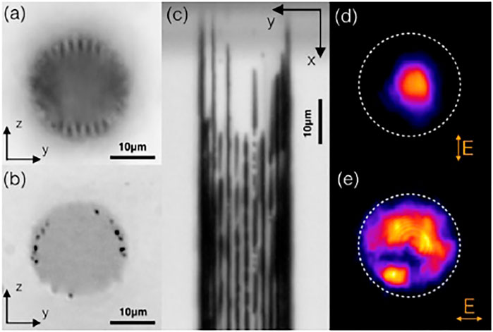
FIGURE 10. (A) Microscopy image of the side surface of the type III waveguide focused under the surface of the sample.(B) Microscopy image of the side surface of the type III waveguide focused on the surface of the sample. (C) Topdown transmission microscopy image of the graphitic tracks comprising the waveguide. Image of the end of the waveguide with (D) vertical and (E) horizontal polarization [55].
In the last few years, active investigations of 3D diamond detectors have been carried out [57, 58]. Femosecond laser processing in the bulk of the diamond [59] leads to the formation of graphitic electrodes. This 3D placement of the electrodes greatly improves the radiation resistance of the detectors compared to conventional electrodes [60]. When machining and fabricating structures in the bulk, the laser beam must focus in the bulk of the diamond. This is quite difficult to do due to the presence of optical aberrations. Due to the refraction of light on the surface of the diamond, there is a depth-dependent shift of focus and a decrease in its intensity [61]. In order to avoid this effect, adaptive optics aberration correction is used to remove distortions [62].
The effect of laser processing parameters on the properties of graphite wires formed inside synthetic mono- and polycrystalline diamonds was investigated [63]. Wires were fabricated in CVD diamond samples using different light polarizations, processing speeds and laser pulse energies. A comparison of their quality was made by measuring their electrical resistance and radius. For many of the columns a barrier potential was observed. The output current was negligible until the applied voltage reached a threshold value. For values of the applied voltage exceeding the threshold voltage the wires exhibited ohmic behavior [63]. Graphite wires with larger diameter and lower resistance and barrier potential were formed with higher pulse energies. The lowest barrier potential and resistance were obtained in wires produced by a large number of repetitions of the graphitization process and slow scanning. The properties of wires were almost independent of the polarization of the laser beam. The correction of the optical aberrations by adaptive optics, aimed to control the laser spot size during fabrication made a great impact on the quality of the formed wires. Applying aberration correction resulted in a negligible barrier potential and a minimum value of the wire resistance. The obtained results were reproduced by multiple measurements [63]. Determining of the barrier potential could be a very important factor for the characterization of graphite wires fabricated by emerging methods, such as the use of Bessel beams [64] as well as for the design of wire junctions [65, 66] or gaps in the conductive network [67].
4 Effect of the Electronic Kinetics on Graphitization of Diamond
Amorphization of diamond by ion irradiation has been experimentally studied by means of spectroscopic or electron microscopy characterization [68–70]. Solid phase transition of diamond induced by femtosecond free-electron laser irradiation has also been evidenced and simulated [71–73]. However, in spite of the comparable level of excitation of the electron system in the femtosecond laser irradiated spots, no noticeable structure transformations were detected in diamond irradiated with swift heavy ions (SHI) [74–78]. This can be ascribed to the conditions of initial excitation–photons vs. ion impact as well as to the difference in the spatial and temporal scales of the initial electronic excitations (10 fs–1 ns and a cylindrical laser spot 1 × 1 μm on the surface of the sample vs. 0.1–10 fs and a diameter 5–50 nm in SHI track of 20–100 μm length). The latter leads to different channels of energy dissipation to the diamond lattice [79].
It has been proposed [80], that in the case of laser excitation, the electron density can be kept above critical for times sufficient for nonthermal melting due to the micrometer scale of the laser irradiated region.
On the contrary, the SHI tracks have an angstrom to nanometric size and due to the very fast lateral spreading of electrons, their density drops quickly. Hence, relatively little energy is transmitted to the diamond lattice in the nanometric vicinity of the SHI trajectory. Due to the high thermal conductivity of the diamond lattice, this excess lattice energy quickly disappears without starting the structural transformations in the SHI track. The lifetime of the excited electronic system during laser irradiation is quite longer, so a large amount of energy is transferred to the diamond lattice. As a result, there are non-thermal effects that destabilize the lattice itself.
A lower level of laser fluence is needed to initiate graphitization in neutron predamaged diamond samples [81]. This points out to a large influence of the concentration of defects on the kinetics of excitation and relaxation of laser irradiated diamond. The neutron-induced defects enhance the coupling of excited electrons with diamond lattice, while decreasing heat diffusion from the laser spot to the lattice itself. Consequently, energies delivered to the electronic subsystem and the lattice and lifetimes of the excitations increase. Finally, this results in an enhanced graphitization of the pre-damaged diamond material, compared to the undamaged one.
5 Overview of Theoretical Modeling
We present an overview of the advanced theoretical approaches aiming at understanding the fundamental physical processes of femtosecond laser interaction with semiconductors and dielectrics that are relevant and important for ultrafast diamond processing applications. In this regime of material modification, the different stages during the transformation of the material properties can be studied using time-resolved techniques. In compementarity to experimental findings, the theoretical methods describe the evolution of strongly nonlinear and non-equilibrium carrier dynamics in diamond and the change of its optical, electronic and structural properties. The ultimate goal is to identify an accurate parameter free theoretical approach suitable for interpretation and prediction of real–time experiments and for establishing of a connection between complex microscopic response and macroscopic properties of the photoexcited substrate.
5.1 Electronic Band Structure
The extraordinary physical and chemical properties of diamond are determined by its crystal structure. Diamond is a Group IV element with six electrons occupying a ground state configuration: 1s22s22p2. Diamond crystal comprises a face-centered cubic lattice structure with a lattice constant equal to the cube edge length a0 = 0.3567 nm. Two carbon atoms which are displaced from each other by a translation of a0 (1/4, 1/4, 1/4) along a body diagonal are associated with each lattice vertex. Each carbon atom forms a strong sp3-hybridized covalent bond with its four neighboring carbon atoms in this regular stable tetrahedral configuration [82]. The C-C bond length is 0.1545 nm at 298 K. The high strength of the C-C bond and its short length are responsible for the extreme hardness of diamond and its large elastic moduli.
The theoretical calculation of the energy band structure of diamond is of key importance for interpreting the material’s optical properties. The band structure represents the allowed energies of an electron as a function of crystal momentum k. The electronic energy gap Eg is defined as the minimum energy required to excite an electron from a filled valence band to an empty conduction band. Pseudopotentials or their form factors were calculated from crystalline energy levels using empirical pseudopotential [83] or nonlocal pseudopotential [84] methods to obtain band structures for Group IV elements for the accurate interpretation of optical reflectivity and photoemission experimental data [85]. Crystalline diamond band structure and electronic properties were calculated applying tight binding model with Hartree-Fock wave functions [86, 87] and two ab initio methods–Hartree-Fock (HF) and density functional theory (DFT) within the generalized gradient approximation (GGA) [88, 89].
The state-of-the-art accurate calculations of the electronic structure of solids combine density functional theory (DFT) [90] and many-body perturbation theory (MBPT) [91]. DFT describes the structure of materials in their electronic ground states and provides reliable initial wave functions and valence eigenenergies, but an unreliable bandgap. For that reason, the DFT wave functions are post-treated by MBPT in the GW approximation to DFT for incorporating many-electron self-energy effects [92]. The combined approach delivers electronic bandgaps within 0.1–0.4 eV of the experimentally obtained ones [93].
Most electronic structure studies are performed for static lattices that are implicitly assumed to be at 0 K. Experimental investigations of material properties, though, are carried out at finite temperatures. Temperature affects the nuclear motion in the material leading to lattice dynamics, which in turn alters the electronic energies in the solid. The electron-phonon interaction whose major contribution stems from the lattice dynamical behavior is included in density functional total energy calculations with ab initio pseudopotentials via the formalism of Allen [94] to obtain the temperature dependent electronic structure of diamond and silicon [95]. An ab initio method based on the all electron quasiparticle (QP) self-consistent (QPSC) GW approximation and Keldysh time-loop Green’s function approach was applied for calculations of diamond electronic structure at finite temperatures [96]. The ground state electronic properties of diamond were calculated from first principles using local density approximation (LDA), generalized gradient approximations (GGA) functionals [97] and an improved quasiparticle self-consistent GW (QSGW) method [98, 99]. In Figure 11, the band structure of diamond for crystal momentum varying along the ΓX and ΓL directions in the Brillouin zone is shown. The empirical pseudopotential model used in the calculation [100] reproduces the principal energy gaps quantitatively. The absolute energy position of the conduction band minimum corresponds to an indirect gap of 5.42 eV. This is in very good quantitative agreement with the experimental result. Since in long-wavelength approximation a momentum changing transition cannot be induced by the laser, the minimal energy required to cross the energy gap at the Γ point is 7 eV.
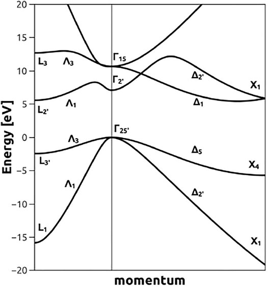
FIGURE 11. Electronic energy bands of diamond along Δ and Λ symmetry lines [100].
5.2 Laser-Induced Processes
An ultrashort laser pulse (10–15 s–10−12 s) generates high peak electric fields (>109 V/m), which are orders of magnitude larger than the Coulomb fields binding electrons to atoms and correspond to laser intensities exceeding 1012 W/cm2. The highest frequency at which the electronic system responds to the strong driving field is determined by the material band gap E g., In this excitation regime, nonlinear absorption for laser frequencies below the direct bandgap energy of diamond is induced and the material absorbs energy from the field due to the creation of electron-hole pairs across the material band gap.
The initial processes following the conventional near-infrared (NIR) to near-ultraviolet (NUV) wavelength ultrashort-pulse laser irradiation of diamond are carrier photoionization and photoexcitation, buildup of coherent polarization and carrier thermalisation. Energy deposited onto the electron system on a timescale shorter than the electron-phonon scattering time may induce ultrafast non-thermal structural changes directly driven by electronic excitation and related non-linear processes. For example, when a certain fraction of valence electrons are excited to the conduction band, they are removed from the bonds and move to the interstitial regions. This causes the weakening of the chemical bonds and affects the cohesion of diamond material. If the electrons diffuse away, the positively charged ions left behind repel each other and cause lattice instability.
On ultrashort time scale, shorter than that of momentum scattering, the generated electrons and holes are described by a coherent superposition of states in the valence and conduction bands. At increased field strength a high number of electron-hole pairs is generated leading to optical breakdown of the material. Ultrafast optical breakdown is a complex, strongly nonlinear threshold phenomenon involving a number of microscopic prossesses and leading to structural modifications of the irradiated material that are highly controllable and reproducible. Conventionally the laser fluence, defined as the time integral of the laser intensity over the pulse length, which produces the critical electron density for which the generated electron plasma becomes reflective, is defined as the optical breakdown threshold (OBT) fluence for the fixed pulse duration [101]. Properly calculated material bandgap and dielectric function near the laser frequency are important for obtaining the OBT. An alternative way to determine the OBT is defined by the averaged kinetic energy deposited onto the electrons [102].
Depending on the pulse duration, scattering with phonons may initiate during the irradiation leading to field-assisted collisional effects (e.g., making possible inditect transitions in conduction band), dephasing of coherence and carrier-phonon scattering. Usually permanent structural effects on the surface including carrier removal and ablation occur for interaction times longer than a picosecond, i.e., after the conclusion of the ultrashort pulse and involves energy transfer between the carriers and the lattice.
5.2.1 Photoionization and Photoexcitation
Photoionization and photoexcitation of electrons are the main mechanisms of laser-pulse energy deposition, which subsequently causes ultrafast transformation of the crystal lattice. The conventional theoretical description of strong-field ionization and interband transitions in solids is based on the Keldysh approach [103–105] that provides an analytical expression for the cycle-averaged interband transitions rate induced by a monochromatic electric field of arbitrary strength. A dimensionless Keldysh parameter relating the bandgap energy of the material with the ponderomotive energy of an electron hole pair is used to separate the interband transitions into adiabatic tunneling, diabatic tunneling and multiphoton excitations. In the adiabatic tunneling regime, the electron goes through the partially suppressed potential barrier without changing its total energy, while in the multiphoton regime transitions occur without any penetration into classically forbidden regions. In the regime of diabatic tunneling the electron wave function cannot adjust to the fast changes of the external potential, so it gradually acquires energy that facilitates its transition into the continuum of conduction states. In this method, the two-band approximation was used, assuming that the electric field predominantly excites electrons from the highest valence band to the lowest conduction band. Second order of two-band k × p-perturbation theory, which provides the dispersion relation between energy and momentum of Bloch electrons, predicted that the band gap monotonically increases with increase of the electron crystal momentum. A nonperturbative parameter which is the ratio of the ponderomotive and photon energies, determines the number of additional photons that must be involved in the excitation of an electron-hole pair in order to overcome the increase of the band gap due to intraband motion. Another key approximation of this theory is the neglect of the Coulomb interaction between an electron excited to the conduction band and the positively charged hole left behind in the valence band.
The transition between adiabatic states, induced by ultrashort laser pulses of arbitrary waveform was studied using quantum mechanical formalism which was a generalization of the Keldysh theory of photoionization [106]. It was demonstrated that electron dynamics in strong field resulted from a nontrivial combination of interband and intraband motion and that photionization depended sensitively on details of the substrate band structure [106]. The Time Dependent Schrodinger Equation (TDSE) in single active electron approximation and velocity gauge, combined with empirical pseudopotential method for realistic band structure calculation, was applied to model the high electronic excitation in CVD polycrystalline diamond irradiated by 30 fs infrared laser pulses with varying intensity below and close to the graphitization threshold [107]. The modeling was carried out under the same conditions as the experimental procedure used to produce three-dimensional conductive paths in the bulk of diamond. It was found that in the weak coupling regime (laser intensity I ∼ 1 TW/cm2) the scaling of the conduction electron density with driving laser intensity strongly deviates from the conventional multiphoton ionization due to Stark effect creating a highly polarizable transient state in the bulk of the material that ionizes very efficiently. In the strong coupling regime (I ∼ 50 TW/cm2), nonadiabatic effects of electron-hole pair excitation result in the generatation of high carrier densities which cause the optical breakdown of diamond. The comparison of theoretical prediction with experimental data of laser-generated charge as a function of laser energy density provides a good quantitative agreement over six orders of magnitude.
An analytical model based on TDSE with a parabolic two-band structure was reported to give consistent results with the experimental data on anisotropy of multiphoton carrier generation in monocrystalline diamond [108]. The energy transfer mechanism from a few cycle intense mid-infrared laser pulse to the electronic system in the bulk of diamond and the subsequent optical breakdown in the material is studied via TDSE with model band structure in [109]. Ultrafast modification of the band structure of wide-band-gap solids was studied using TDSE in length gauge [110]. In [107–109] dipole approximation was used and electron-electron and electron-phonon collisions were neglected.
The density matrix method leading to Semiconductor Bloch equations (SBE) for the time evolution of electron and hole occupations and microscopic polarization was applied to describe interband and intraband carrier excitation and ultrafast dephasing in semiconductors and diamond in particular [111–114]. This approach requires input parameters on various levels of sophistication and can incorporate a different number of energy bands. For example quasi-energies are defined for a single electron (hole) in the crystal lattice and they are modified when Coulomb interaction of carriers is included in the model. SBEs are derived within the Hatree Fock approximation and they incorporate many-body Coloumb effects and phase-space filling. Going beyond this approximation requires higher-order correlation functions leading to further renormalization of interactions and energies.
Time-dependent density functional theory (TDDFT) [115] as an extension of DFT provides the band structure of diamond and describes the real time-dependent quantum dynamics of interacting electrons at the first-principles level treating the mechanisms of multiphoton and tunneling ionization and including dynamical screening. Norm-conserving pseudopotentials are used to account for the interactions between the valence electrons and the ionic cores. The static Kohn-Sham equation is first solved to determine energy bands, density of states, and forces acting on the ions in the ground state. The time evolution of the electronic orbitals is obtained following the excitaion of the time-dependent spatially uniform electric field of the ultrashort-pulsed laser. The transmitted field inside the bulk substrate includes the polarization field of the medium. Since semi-local exchange correlation functionals are used in the calculations, i.e. the adiabatic local-density approximation (ALDA) or generalized gradient approximations (GGA), the method is limited for pulse durations shorter than the electron-electron and the electron-phonon relaxation time. The relaxation related to energy transfer from electrons to ions was also ignored. In [115] 16 fs laser pulses with varying wavelengths were used to determine optical breakdown in diamond. It was found that when laser intensity is low diamond exhibits dielectric response with static dielectric function obtained from the ratio of the external to the total electric field. It was shown that in the weak coupling regime the energy deposition in diamond as a function of intensity follows the perturbative scaling wich agrees with Keldysh theory. For peak laser intensities (I > 70 TW/cm2), the deposited energy exhibits abrupt increase which is consistent with resonant energy absorption when optical breakdown occurs. This effect is also exhibited by the phase shift between the total electric field and the applied electric field. The optical breakdown, reached when plasma frequency matches the laser frequency, is found to be limited by emerging plasma oscillations at the conclusion of the laser pulse and screening of the electrons in the conduction band. In [116] electronic excitation in diamond following the irradiation of intense ultrashort laser pulse was investigated by TDDFT for various wavelengths and laser intensities in order to describe the energy transfer mechanisms. The calculated results were compared with the excitation rates from Keldysh theory and with the energy deposition rates in other dielectric materials possessing different bandgap energies and cohesion mechanisms.
The strong non-linear and ultrafast dynamics of electrons results in high-order harmonic generation [100, 117–120] and in optical-field-induced transient and reversible currents below the bulk damage threshold [121–124]. It was experimentally found and theoretically confirmed [113] that high harmonic generation in bulk solids is characteristic of a nonperturbative quantum interference process that involves electrons from multiple valence bands. Photoexcitation, nonlinear optical properties, induced ultrafast currents and generation of high harmonics in diamond irradiated by ultrashort infrared ultrashort laser pulses were described by an extended TDDFT accounting for coupling of the excited electronic system to external (“environmental”) degrees of freedom that could be phonons or lattice defects. The results of the calculation were compared with the results from SBE calculation [120].
5.2.2 Optical Properties
The electric fields of ultrashort intense laser pulses are able to modify the optical properties of a solid substantially and nondestructively. The transient changes of optical properties provide valuable information on the prompt changes of electronic and atomic structure of irradiated solids. The optical response of band gap materials varies with the driving laser intensity. For low peak intensities a dielectric response is exhibited. With increase of intensity, nonlinear response prevails and high-order perturbation theories should be used for calculating the response in the frequency domain [125]. For very strong electric fields of the laser the material’s optical properties become similar to those of a nonequilibrium electron-hole plasma [126]. In the strong coupling regime the polarization response of a solid is no longer described by a set of linear and nonlinear susceptibilities and should be modelled quantum mechanically using Shrodinger equation which is only feasible in one or two active electrons approximation for the treatment of many electron systems hence approximations are required. As described in previous sections, density functional theory (DFT) with an approximated semi-local exchange and correlation functional is used to describe electrons in the ground state and time-dependent DFT (TDDFT) is required to simulate excited electrons. For electron dynamics, the real-time formulation of TDDFT can account for response to strong perturbations. Going beyond TDDFT it is possible to describe more precisely optical properties of solids, for example by using the time dependent Bethe–Salpeter equation. The optical responses of infinitely periodic systems to a spatially uniform external field are characterized by the complex dielectric function.
Non-local empirical-pseudopotential method was used to calculate the optical absorption in type I diamond [84] and a good agreement with the position of the main peak of the imaginary part of the complex dielectric function was found but its magnitude showed a significant discrepancy with experiment. The momentum and energy dependent Lindhard dielectric function of diamond was obtained using full band calculation based on the local empirical pseudopotential method [127] via MC calculation. The frequency-dependent dielectric functions for the crystals in the diamond lattice structure were obtained by a real-space approach to TDDFT within the adiabatic local-density approximation, implementing full-potential linear combination of atomic orbitals (LCAO). The dielectric constants at optical frequencies were also obtained and were in good agreement with experiments. It was found that the calculated dielectric functions reproduced accurately the experimental spectral features [128]. The linear response of diamond was calculated via TDDFT using a real-space representation of the electron wave functions and calculating the carrier dynamics in real time [129]. After obtaining the ground-state electron orbitals and the periodic Coulomb potential in the absence of an electric field, an impulsive external electric field was applied and the polarization electric field was determined by the real-time evolution of the time dependent Kohn Sham (TDKS) equation. The inverse frequency dependent dielectric function was related to the Fourier transform of the total electric field (including the induced polarization field). This approach was further developed and the frequency dependent electric conductivity and the dielectric function of a group IV semiconductor were obtained by solving the TDKS equation for the electron dynamics following the excitation of a pump pulse. It was shown that the real part of the dielectric function exhibits a metallic like response at low frequencies reflecting the generation of dense electron-hole pair excitations [130]. Similar approach was applied for the manipulation of the dielectric function of diamond in nonequilibrium state induced by an intense and single-cycle ultrafast laser field with duration of a several femtoseconds [131]. As in the previous study for silicon [130], for high intensities negative divergence of the real part of the dielectric function at low frequencies was observed. The anisotropy of dielectric tensor in excited diamond when going beyond the linear response regime was also demonstarted [131]. Using real-space, real-time TDDFT calculations it was demonstrated that the permittivity tensor of the diamond can be effectively tuned by an ultrashort laser pulse to exhibit hyperbolic or elliptic response for a particular light frequency [132].
The time-dependent subcycle modulation of the dielectric function close to the energy gap of diamond was calculated by TDDFT in the frame of a numeric pump-probe experiment as a manifestation of the time-resolved Dynamical Franz Keldysh effect (Tr-DFKE). This ultrafast modulation was found to be phase shifted with respect to the applied probe field [133]. The sub-femtosecond optical response of polycrystalline diamond irradiated by intense, 250 attosecond pump pulses was studied by transient absorption spectroscopy. It was shown that the infrared pulse induces oscillations in the imaginary part of the dielectric function and consequently in the absorbance of the material. Ab initio calculations performed by coupling time-dependent density functional theory (TDDFT) in real time with Maxwell’s equations reproduced the experimental results [134]. Experimental and theoretical results showed that the strong field induces tens of orders of magnitude increase of the conductivity that may lead to a state of semi-metallization, which is reversible on a femtosecond time scale [135].
The complex dielectric function and transient optical properties such as reflectivity, transmission and absorption were calculated by a hybrid MC method [136] and it was shown that they could be used for diagnostics of electronic and structural transitions occurring in irradiated semiconductors.
In [38] the dielectric function of diamond irradiated with 515 fs infra red laser pulse was obtained via the time-dependent plasmon pole-approximation for the density-density correlation function of coulombically interacting electron gas assuming that the linear response of photoexcited diamond can be described by a free-carrier Drude response. Most recently, the linear response and the modulation of optical properties of diamond were calculated using a multiscale method combining self-consitenly Time dependent Kohn Sham equation to describe microscopic electron dynamics, Maxwell equations to describe macroscopic propagation of the laser pulse and first-principles Ehrenfest (classical) Molecular dynamics approach to describe the ultrafast lattice dynamics [137, 138].
A first principles method was used (GW approximation to DFT and an effective Hamiltonian including the electron-hole interaction extracted from Bethe-Salpeter equation for the electron-hole pair wave function) to determine the frequency-dependent imaginary part of the dielectric function in diamond by iteratively applying the effective Hamiltonian on an electron-hole pair state [139]. Recently the optical absorption spectra for diamond were obtained through TDDFT based on nonempirical hybrid functionals that were designed to correctly reproduce the dielectric function. The comparison with the combined state-of-the-art GW calculations and the Bethe-Salpeter equation (BSE-GW) shows close agreement for the transition energies and the main features of the spectra [140].
5.2.3 Imapact Ionization and Auger Recombination
After photoelectrons are excited into the conduction band across the direct band gap (with well defined energies above the conduction band minimum) they experience electron-electron collisions, while absorbing additional energy from the laser field. If a substantial fraction of the carriers occupy higher lying conduction bands with energy above the threshold for impact ionization (specified by the indirect gap of diamond equal to 5.4 eV), the highly energetic electrons can collisionally ionize electrons into lower energy states. Following the collision, the impact electrons lose part of their energy, transferring it to promote valence electrons in the conduction band. Thus, once a threshold energy is reached by conduction electrons, impact ionization (II) may occur on a femtosecond time scale resulting in carrier multiplication through the decay of high energy electrons into lower energy states while generating electron-hole pairs [141]. When carrier densities become high Auger recombination (AR), related to impact ionization through the principle of detailed balance as an inverse microscopic prossesses, may become significant. In a direct Auger process, an electron recombines with a hole, but instead of emitting a photon the process results in the excitation of another carrier to a higher-energy state [141].
The impact ionization rate in diamond was calculated by Monte-Carlo (MC) simulation which included a band structure obtained from an empirical pseudopotential method and frequency- and momentum-dependent Lindhard dielectric function [127]. Recently the ultrafast impact ionization in diamond irradiated by mid-infrared femtosecond laser pulses was experimentally observed by transient transmission spectroscopy and photoluminescence measurements [142] revealing that the excited carrier population incerases two times in comparison to the initial one for peak intensity of 2.5 TW/cm2. Supporting TDDFT simulations of electron dynamics showed that the photoexcited carriers could reach the energy threshold for impact ionization in diamond under the experimental conditions. Scattering mechanisms were not included to describe theoretically ultrafast impact ionization. Even though the kinetic energy distribution of the photoexcited carriers in CVD diamond extended above the required threshold, the process of impact ionization was strongly suppressed by the high population of the conduction-band low-energy states due to Pauli blocking and electrons could gain sufficiently high energies from the laser field [107]. A first-principles approach based on screened exchange density functional theory (DFT) was applied for the calculation of II and AR rates in semiconductors [143]. MC techniques were used to calculate impact ionization and Auger recombination rates in diamond [71] irradiated by X ray femtosecond pulses.
On ultrashort time scale, photoionization alone or together with ultrafast impact ionization generate high electron-hole plasma density, leading to multiplication of conduction electron number and an efficient energy transfer from the laser to the conduction electrons. When the absorbed laser energy exceeds the melting or cohesive energy of the material, optical breakdown occurs which is also considered as a precursor to laser ablation. In [38] for the 200 fs pulse duration used in the experiment and intensities lower than 50 TW/cm2 it was found that the electron density produced by photoionization is below the critical one. The calculated density of conduction states at the end of the pulse showed that substantial fraction of carriers occupy higher lying conduction bands with energy above the threshold for impact ionization and may collisionally promote valence electrons in the conduction band. The intensity-dependent impact ionization rate was obtained as a weighed average of the field-free rate [127] using the calculated density of conduction states in diamond.
5.2.4 Coherent Phonon Generation and Ultrafast Phase Transitions
As shown in the experimental part of the review it is important to know on what time scale the structural transformations occur. Since the typical electron-lattice energy relaxation time is 10–10–10–12 s, the incident femtosecond laser pulse deposits energy onto the electron system creating a transient highly non-equilibrium state in which initially the nuclei remain fixed at the lattice positions and electronic excitation and vibrational degrees of freedom are completely decoupled. Consequently, the laser induced redistribution of the electronic occupation modifies the interatomic bonding that results in coherent phonon generation [137, 138, 144–147], solid-to-solid phase transitions [148, 149], thermal phonon squeezing [150], and nonthermal melting [151–153].
Femtosecond time-resolved pump-probe reflection experiments in semiconductors revealed large-amplitude oscillations with periods that were characteristic of lattice vibrations. The frequency of the oscillations in the observed reflection matched one of the optical phonon modes, which indicated that this particular phonon mode was coherently excited. Under the assumption that the electronically excited system rapidly comes to quasiequilibrium in a time shorter than nuclear response times, a theoretical model of displacive excitation of coherent phonons (DECP) describes the evolution of a coherent phonon amplitude in the presence of nonequilibrium photocarriers with driving force, which is a function of the carrier density and the temperature of the carrier distribution. A rapid increase in the carrier density during the optical excitation, initiates the oscillating motion of the coherent amplitude [144]. The excitation of coherent optical phonons was modeled via adiabatic TDDFT [146]. It was theoretically predicted by ab-initio molecular-dynamics simulations [150] that femtosecond-laser-induced collective atomic motions precede complete atomic disordering (nonthermal melting) as a function of laser fluence. The instability of the diamond and zinc-blende structures due to the excitation of a dense electron-hole plasma were described under the assumption that the photo-excited plasma thermalizes rapidly, due to the strong electron-electron interaction. Its effect on the cohesive energy of the diamond structure together with the lattice distortions caused by phonons were analyzed [154]. When a substantial fraction of electron–hole pairs is generated in the material, there is a strong modification of the electron density distribution. Consequently, the ions experience strong repulsive inter-atomic forces due to the dramatic changes of the potential energy surface (PES). Using a tight binding Hamiltonian for the electronic occupations it was shown that the functional form of the potential energy surface (PES) strongly depends on the occupation of the electronic levels. The modified interatomic forces can cause coherent atomic motions. If they are sufficiently strong, they can induce permanent structural modification of crystalline diamond on a very short time scale [73, 144, 155–157] without invoking significant energy transfer between electrons and ions and without significant increase of the ionic temperature. Hence, the ultrafast disordering was regarded as nonthermal phase transition [158, 159]. Density functional theory approaches were used to account for the changes in the PES following electron–hole-pair excitation [160, 161]. Laser excited ab initio PES was obtained under the assumption that the electronic system has a particular temperature following the excitation and the subsequent thermalization. Thus, electronic occupations were considered to obey a Fermi distribution at the resulting electronic temperature and Kohn–Sham equations were solved self-consistently under this constraint. The electronic entropy was determined and PES was obtained by applying a generalized Born–Oppenheimer approximation. Recently a numerical pump-probe multiscale calculation was used to simulate coherent phonon generation in diamond [137]. The calculations demonstrated that the driving force on the ions of the crystal lattice was generated as a consequence of the change in the electron density which was dependent on the strength of the applied field and did not arise from the direct laser field-ion interaction. The ground state electron density in the (011) plane of diamond was compared with the transient electron density induced by the ultrashort laser pulse excitation. It was demonstrated that the applied field induced a shift in the electron bonding direction in respect to the ground state in which the covalent bonds were situated between the ions of the lattice. The shift was dependent on the direction of the applied electric field. It was also found that the forces exerted on the ions were independent of the field direction and all the ions in the chosen plane of the material were weakened. It was found that the generated coherent phonons induced anisotropy in the refractive index of diamond as well as a modulation in the reflection of the probe pulse [138].
5.2.5 Carrier Relaxation
For times greater than 10–12 s, the energy absorbed by the electronic subsystem dissipates into the ionic degrees of freedom via electron-phonon coupling, causing the ionic temperature to increase. The ionic temperature can rise beyond the melting point, which would result in the disordering of the lattice in few picoseconds. This transition is ultrafast thermal melting since conduction electrons can cause a permanent structural damage of the material by transferring their kinetic energy to the lattice. At these time scales the ultrafast dynamics of photocarriers in irradiated semiconductors was described by theoretical methods varying from model equations using parametrization of the distribution functions [162–165], direct integration of Boltzmann equation [166,167] or Monte Carlo simulations [168–171]. Calculation approaches were chosen based on their ability to include and interpret on microscopic level the carrier-carrier and carrier-phonon scattering processes, which strongly depend on the experimental conditions (e.g., electron-electron effects depend on the conduction electron density). Complementarity of experimental results and theoretical calculations provide relevant data on the required scattering rates and coupling constants [172–174].
On short time scales, both coherent and incoherent processes have to be included. The buildup of polarization and the Coulomb interaction between carriers requires a full quantum mechanical treatment. Quantum kinetic theoretical methods used to describe the coherent phenomena are non-equilibrium Green’s-functions techniques [172–174] and density-matrix theory [175, 176]. For time dependent processes such as ultrashort-pulsed laser irradiation of semiconductor materials the density matrix method provides quantities directly comparable with physical observables.
Quantum kinetic-type approaches, two temperature models and rate equations have been applied to account for all main relaxation processes [177–179]. In quantum-kinetic approach, the starting point is a Hamiltonian that describes the electron and the phonon subsystems and their coupling to first and second order in the atomic displacements using second-quantized formalism. The matrix elements in the Hamiltonian provide the strength of the coupling between the electron and the phonon subsystems. This approach has important shortcomings when used for predictive calculations, because the electronic part Hamiltonian relies on the assumption that the studied system can be described in terms of well-defined quasiparticle excitations and that the phonon term is included within the harmonic and the adiabatic approximations. In addition, the single-particle eigenvalue of an electron with a crystal momentum k in a band n, the frequency of a lattice vibration with crystal momentum q in the branch λ, the phonon dispersion and the strength of the coupling between the electron and the phonon subsystems have to be determined using other methods. Phonon dispersion relations, electron phonon coupling strength and electron-phonon matrix elements in diamond can be calculated using Density Functional Theory, entirely from first principles [180–183]. In addition, nonadiabatic corrections to phonon dispersion relations and temperature dependence of optical spectra in direct and indirect-gap semiconductors can be obtained. Density functional perturbation theory DFPT enables the calculations of vibrational frequencies and eigenmodes at arbitrary wave vectors in the Brillouin zone. Electron-phonon scattering processes and electron-phonon renormalization of band structure can be computed from the lattice dynamical properties obtained from DFT or DFPT within the local density approximation (LDA) [184–191]. Combined with the Boltzmann or the Kadanoff-Baym equations [189–191], the dynamics in materials can be studied. The temperature-dependent renormalization of the direct band gap of diamond arising from electron-phonon interactions and the temperature-dependent broadening of the direct absorption edge in the material were calculated in [186]. The unperturbed band structures were obtained from DFT within the GW approximation, and the lattice dynamics was described within density-functional perturbation theory.
In DFT approach though, the evaluation of the electron-phonon matrix elements uses the assumption that the interaction between electrons and nuclei is governed by the effective Kohn-Sham potential and depends on the exchange and correlation functional. The definition of phonons relies on the Born- Oppenheimer approximation. Since electron-phonon interaction can modify both the electronic structure and the lattice dynamics of a solid, and these modifications will in turn affect the coupling between electrons and phonons, a complete theory of interacting electrons and phonons must be self-consistent.
More elaborate first principle approaches based on many-body perturbation theories discussed in previous sections, provide an ab initio description of both the photo-excitation and of the time dependence of the carrier scattering rates. They allow including on the same footing the change of carrier and phonon populations due to both excitation and scattering which for the case of ultrashort laser pulse excitation may overlap in time. Approaches such as many body Green’s functions and GW plus Bethe Salpeter equation [192,193] may provide accurate parameter-free interpretation of real time pump-probe experiments used to capture electron excitation, electron spatio-temporal distribution on the femtosecond scale, transient optical response, the electron collision time and laser-induced electron-hole plasma lifetime [194, 195]. A first-principles version of the Kadanoff-Baym equations [196,197] employing collision approximation [198] to reduce the non-equilibrium Green’s function dynamics to a single time variable was used to reproduce the carrier dynamics in bulk silicon as observed in a two photons photo-emission experiment. The equation for the evolution of the non-equilibrium electron (hole) occupation contains a coherent generation term, which describes the creation of carriers via the interaction of the polarization and the laser electric field, and a term describing how carriers dissipate energy. This equation is coupled to the polarization equation self-consistently. The generation term is derived from Green’s functions approach based on DFT Kohn-Sham Hamiltonian and includes Hartree and exchange correlation effects. The expressions for carrier-carrier and carrier phonon lifetimes that govern the carrier relaxation include the statically screened Coulomb interaction and the screened ionic potential derivatives, calculated within density-functional perturbation theory [199, 200] and formally correspond to the carrier-carrier and carrier-phonon scattering in the semi classical Boltzmann equation obtained using Fermi Golden Rule. The dependence of the relaxation terms on the calculated occupations was obtained self consistently at each time step.
5.2.6 Ultrafast Laser Ablation
Laser ablation is a complex phenomenon that includes the initial stage of carrier photoexcitation, collisional ionization, thermalization and relaxation and the transition stage of development of structural changes and removal of matter. Ultrafast laser ablation in diamond was studied experimentally and theoretically [22, 24, 201–211]. In [201] femtosecond time resolved reflectivity and transmission pump-probe measurements of the laser excited substrate indicated an ultrafast melting transition from crystalline diamond to a highly reflective dense plasma. The threshold fluence for ablation of diamond with 620-nm, 90-fs laser pulses was found to be 0.6 J/cm2. Raman spectra and SEM images of CVD diamond ablated with a number of femtosecond laser pulses near threshold fluence revealed no evidence of graphite or amorphous carbon and clean ablation with sharp interfaces and little thermal damage. In [202] molecular dynamic simulations performed on the basis of time-dependent, many-body potential energy surfaces derived from a microscopic electronic Hamiltonian were used to obtain laser induced femtosecond structural changes in diamond. The results showed smoothly increasing ablation threshold for increasing pulse duration. In [212] the optical damage and surface ablation threshold fluences as a function of pulse width for femtosecond laser irradiated silicon oxide were obtained from a TDDFT calculation. The threshold fluence for optical damage was determined by comparing the transferred energy to the energy needed to melt the quartz substrate. The calculated ablation threshold fluence was compared to experimental data to demonstare the significance of the nonthermal ablation mechanism and the agreement between the measured and theoretically calculated ablation craters.
First-principles electromagnetic theory predicted that when the laser fluence exceeds that of the ablation threshold, laser induced periodic surface structures (LIPSS) can be formed [213] as a universal phenomenon. It was shown that the periodicity of the formed ripples was close to the laser wavelength and orthogonal to the laser polarization. Near-wavelength ripples (low-spatial-frequency LIPSS–LSFLs) can be formed when a small number of intense pulses irradiate semiconductors and dielectrics via inhomogeneous energy deposition resulting from the interference between the femtosecond laser pulse scattered on permanent or laser-induced (phase transition of diamond to carbon phase) surface relief roughness and the incident pulse [214]. For irradiation with femtosecond laser pulses, in the regime of optical breakdown fluences, the photogenerated dense electron-hole plasma (EHP) induces a transient change of the optical properties (the permittivity) of the substrate surface and it exhibits metallic behavior [215]. The interaction of the incident pulse with the photogenerated plasma at the interface between the insulator and the conductor leads to plasma oscillations coupled to electromagnetic fields, which can support a highly confined surface electromagmetic wave–surface plasmon (SP). These short wavelength longitudinal surface plasmons could also interfere with the incident laser pulse or among themselves inducing surface ripples with periods much lower than the laser wavelength [35, 216].
The transition of diamond into plasmonically active material and the subsequent formation of ripples on its surface caused by SPP-laser interference were investigated via first principle approaches [41]. The numerical modeling of periodic laser energy deposition on photo-excited diamond surface showed the formation of fine ripples oriented perpendicularly to the laser polarization in a narrow range of intensities above the optical breakdown threshold. The transient increase of the carrier density above this threshold resulted in the formation of near-wavelength surface ripples. Quantitative agreement with the experimentally observed periods of the periodic structures was obtained. The transient efficacy factor describing the efficacy with which the preexisting surface roughness induces inhomogeneous energy absorption at the LIPSS wave vector κ = (κx, κy) incorporated the variation of the dielectric constant of the photoexcited diamond. The two dimensional efficacy factor map of LIPSS formation as a function of the normalized LIPSS wave vector components is shown in Figure 12 for two values of the transient bulk plasma frequency in monocrystalline diamond irradiated by a 515 nm, 200 fs laser pulse [41]. LIPSS were formed where the efficacy factor map exhibits sharp features (minima and maxima). In Figure 12A for laser frequency ωL close to the surface plasma frequency ωp, the efficacy factor has large contribution due to excitation of the surface plasmon resonance. In this regime, the deposition of laser energy at the surface plasmon wavevector favors the formation of fine ripples with spatial periods around 100 nm. Figure 12B shows that when the transiently increasing electron-hole plasma number density results in large and negative value of the dielectric constant at the laser wavelength, the observed feature in the efficacy map is a circle with κ = 1 and can be associated with the formation of near-wavelength surface ripples oriented perpendicularly to the laser polarization.
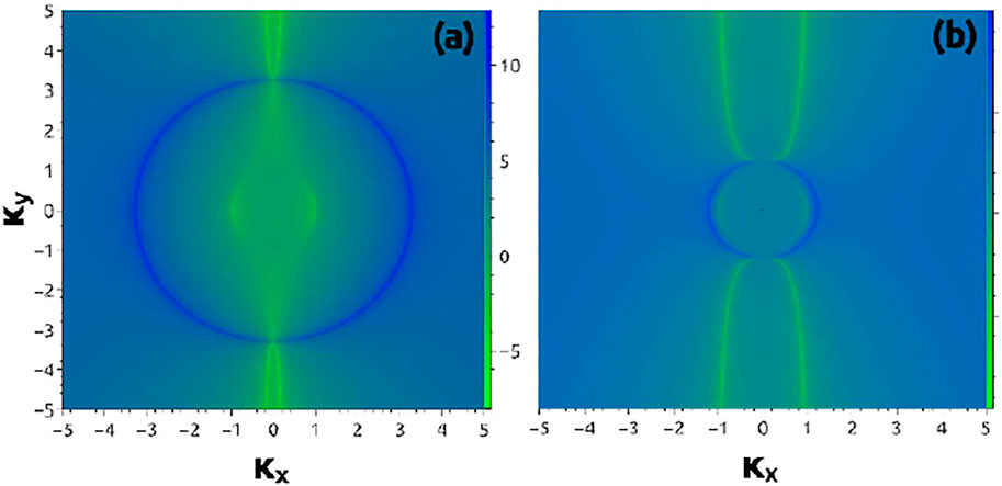
FIGURE 12. [41] Two dimensional intensity graph of the logarithm of diamond transient efficacy factor as a function of the normalized to the laser wavelength LIPSS wave vector components. In (A) ωp = 1.5 ωL and (B) ωp = 1.5 ωL.
5.2.7 Summary and Outlook
In the experimental part of our review, it was revealed that ultrashort intense laser pulses provide a unique technique for precise diamond micromachining, mainly due to high electric field strengths capable of inducing nonlinear absorption in transparent wide band gap materials as diamond, due to minimized thermal effects and due to short processing times. It was demonstrated that this technique could be used for effective surface nanostructuring or fabrication of three-dimensional structures inside diamond, which allows rapid prototyping of integrated photonic and electronic devices such as photon-enhanced thermionic emitters, electrochemical electrodes and sensors. The confinement of the laser energy absorption to the focal volume situated on top of or inside the bulk of the material is performed experimentally by tight focusing and by tuning the laser parameters such as wavelength, energy density, pulse repetition rate, angle of incidence and polarization state. Surface nanostructuring results in significant modifications of the optical and electronic properties of diamond. One major experimental result is tailoring the optical transmissivity of diamond surfaces via creating laser induced periodic surface structures (LIPSS) with high degree of accuracy of structure periodicity, morphology and aspect ratio achieved by varying the laser parameters. An important experimental result is the fabrication of three-dimensional buried optical waveguides in diamond by focusing high repetition rate femtosecond laser pulses in the material. Despite this innovative capability, the fabricated waveguides still have high extinction coefficient.
Highly conductive graphitic wires with resistivity approaching that of polycrystalline graphite and capable of following any 3D path were fabricated in diamond. Conductive nanostructures of graphenic carbon were produced inside single crystal diamond by femtosecond laser irradiation and the ratio between the sp3 and sp2 carbon in the laser-modified heterophase was estimated. These achievements are directly applicable to the design of three dimensional diamond detectors. The current drawback is that diamond detectors with three-dimensional architecture are strongly limited by the excessive resistivity of the columnar electrodes, which increase the noise of the response and degrade the time resolution. The issue for three-dimensional diamond dosimeters is the uniformity of response of the single pixels, which is impaired by the uncontrolled properties of the columnar electrodes and the surrounding diamond lattice subjected to a high stress condition due to the lower density of the formed sp2 phase. As a major improvement of these issues, namely reducing the electrode resistance, the design, the fabrication and the characterization of timing 3D diamond sensors, with electrodes obtained through a pulsed laser graphitization technique combined with the application of adaptive optics was achieved recently.
In the theoretical part of the review, it is revealed that both mature theoretical and computational methods and advanced time resolved experimental techniques contribute to the fundamental understanding of the microscopic processes involved in ultrafast processing of diamond as a wide band gap semiconductor. The mechanisms are essentially governed by femtosecond pulsed laser-electronic system interaction that can trigger ultrafast electronic, optical and material response and affect the pulse propagation in the modified medium.
Some of the advanced theoretical methods can be used to model successfully the conditions for occurance of ultrafast phase transitions, optical breakdown and ablation in diamond starting from the material’s ground state band structure, and accurately describing initial carrier excitation and subsequent carrier dynamics induced by the ultrafst intense irradiation. Typically the calculations provide time- (and space)- dependent electron density and current, polarization, electronic excitation energies, energy deposited in a unit cell of the substrate, number density of excited electron-hole pairs, transient distribution function of conduction photoelectrons, and forces acting on the ions as functions of time. Optical properties are described at a different level of sophistication. Multiscale models are developed which include self-consistent description of carrier and lattice dynamics and pulse propagation.
The importance of treating some of the involved microscopic processes on an equal footing is demonstrated in view of achieving a deeper theoretical insight and guidance to experiments. Part of the advanced approaches incorporate at first principles level scattering and relaxation processes occurring in parallel with or following carrier ionization and excitation. Limitations of the described theoretical approaches are pointed out and the possibility of interfacing some of methods are discussed.
For instance, in order to engrave three dimensional electrodes in diamond bulk for the design of radiation sensors, extremely short laser pulses are used. In this irradiation regime, close to the experimental conditions, theoretical description of the phase transformation from diamond to conductive phase in the bulk of the material might be closely achieved using the first principles multiscale methods. On the other hand, it is critical for the applications to control the connection between conductive domains, which can be realized via laser annealing of the modified material. In this case it is important to use the first principle approaches based on many-body perturbation theories which successfully describe coupled electron and phonon dynamics. Recent developments in these approaches could also help predict and control the number of defects induced in the diamond bandgap during fabrication which is also of paramount importance for the efficiency of the produced devices.
Author Contributions
VK and IG contributed to the review of experimental methods and TA contributed to the review of theoretical models, some of the experimental methods and the overall text of the manuscript.
Funding
The authors VK and IG declare that this study received funding from NoviNano Lab, LLC (Ukraine). The funder had the following involvement with the study: the description of part of the experimental data.
Conflict of Interest
VK and IG are employees of NoviNano Lab, LLC.
The remaining author declares that the research was conducted in the absence of any commercial or financial relationships that could be construed as a potential conflict of interest.
Publisher’s Note
All claims expressed in this article are solely those of the authors and do not necessarily represent those of their affiliated organizations, or those of the publisher, the editors and the reviewers. Any product that may be evaluated in this article, or claim that may be made by its manufacturer, is not guaranteed or endorsed by the publisher.
Acknowledgments
The authors acknowledge Cost Action CA17126. Support is acknowledged from the Bulgarian National Science Fund under Contract No. KP-06-KOST, No. DN-18/7 and No. DN-18/11 (TA). T.A. expresses gratitude to Professor S. Sciortino from the Department of Physics of Florence for useful discussions on the experimental aspects of the physics of laser-irradiated diamond.
References
1. Prelas M, Popovici G, Bigelow L. Handbook of Industrial Diamonds and Diamond Films. New York: Marcel Dekker (1997).
2. Coe SE, Sussmann RS. Optical, Thermal and Mechanical Properties of CVD Diamond. Diamond Relat Mater (2000) 9:1726–9. doi:10.1016/s0925-9635(00)00298-3
3. Isberg J, Hammersberg J, Johansson E, Wikstrom T, Twitchen DJ, Whitehead AJ, et al. High Carrier Mobility in Single-Crystal Plasma-Deposited Diamond. Science (2002) 297:1670–2. doi:10.1126/science.1074374
4. Chen Y-C, Salter PS, Knauer S, Weng L, Frangeskou AC, Stephen CJ, et al. Laser Writing of Coherent Colour Centres in Diamond. Nat Photon (2017) 11:77–80. doi:10.1038/nphoton.2016.234
5. Chen Y-C, Ishmael SN, Lekhai Y, Johnson S, Stephen CJ, Green BL, et al. Laser Writing of Individual Nitrogen-Vacancy Defects in diamond with Near-unity Yield. Optica (2019) 6:662. doi:10.1364/optica.6.000662
6. Konov VI. Laser in Micro and Nanoprocessing of Diamond Materials. Laser Photon Rev (2012) 6:739–66. doi:10.1002/lpor.201100030
7. Kuznetsov AI, Miroshnichenko AE, Brongersma ML, Kivshar YS, Luk’yanchuk B. Optically Resonant Dielectric Nanostructures. Science (2016) 354(6314):aag2472. doi:10.1126/science.aag2472
8. Ozkan AM, Malshe AP, Railkar TA, Brown WD, Shirk MD, Molian PA. Femtosecond Laser-Induced Periodic Structure Writing on Diamond Crystals and Microclusters. Appl Phys Lett (1999) 75:3716–8. doi:10.1063/1.125439
9. Pham M, Saraeva N. Ultrafast Photoionization and Excitation of Surface- Plasmon-Polaritons on Diamond Surfaces. Commun Phys (2016) 26.
10. Ivanova AK, Ionin AA, Khmelnitskii RA, Kudryashov SI, Levchenko AO, Mel’nik NN, et al. Laser Ablative Decoration of Micro-diamonds by Gold Nanoparticles for Fabrication of Hybrid Plasmonic-Dielectric Antennae. Laser Phys Lett (2017) 14:065902. doi:10.1088/1612-202X/aa6c1a
11. Boltasseva A, Atwater HA. Low-loss Plasmonic Metamaterials. Science (2011) 331:290–1. doi:10.1126/science.1198258
12. Jahani S, Jacob Z. All-dielectric Metamaterials. Nat Nanotech (2016) 11:23–36. doi:10.1038/nnano.2015.304
13. Pan L, Kania D. Diamond: Electronic Properties and Applications. Springer Science and Business Media (2013).
14. Amaratunga GAJ. A Dawn for Carbon Electronics. Science (2002) 297(5587):1657–8. doi:10.1126/science.1075868
15. Shimano R, Nagai M, Horiuchi K, Kuwata-Gonokami M. Formation of a High T(c) Electron-Hole Liquid in diamond. Phys Rev Lett (2002) 88:057484. doi:10.1103/physrevlett.88.057404
16. Kozák M, Trojánek F, Popelář T, Malý P. Dynamics of Electron–Hole Liquid Condensation in CVD diamond Studied by Femtosecond Pump and Probe Spectroscopy. Diam Relat Mater (2013) 34:13. doi:10.1016/j.diamond.2013.01.008
17. Tokuda N, Umezawa H, Yamabe K, Okushi H, Yamasaki S. Growth of Atomically Step-free Surface on diamond {111} Mesas. Diamond Relat Mater (2010) 19:288–90. doi:10.1016/j.diamond.2009.11.015
18. Burns RC, Hansen JO, Spits RA, Sibanda M, Welbourn CM, Welch DL. Growth of High Purity Large Synthetic Diamond Crystals. Diamond Relat Mater (1999) 8:1433–7. doi:10.1016/s0925-9635(99)00042-4
19. Spitsyn BV, Bouilov LL, Derjaguin BV. Vapor Growth of Diamond on Diamond and Other Surfaces. J Cryst Growth (1981) 52:219–26. doi:10.1016/0022-0248(81)90197-4
20. Talamonti C, Kanxheri K, Pallotta S, Servoli L. Diamond Detectors for Radiotherapy X-Ray Small Beam Dosimetry. Front Phys (2021) 9:112. doi:10.3389/fphy.2021.632299
21. Schreck M, Gsell S, Brescia R, Fischer M. Ion Bombardment Induced Buried Lateral Growth: The Key Mechanism for the Synthesis of Single Crystal Diamond Wafers. Sci Rep (2017) 7:44462. doi:10.1038/srep44462
22. Shirk MD, Molian PA, Malshe AP. Ultrashort Pulsed Laser Ablation of Diamond. J Laser Appl (1998) 10:64–70. doi:10.2351/1.521822
23. Okuchi T, Ohfuji H, Odake S, Kagi H, Nagatomo S, Sugata M, et al. Micromachining and Surface Processing of the Super-hard Nano-Polycrystalline diamond by Three Types of Pulsed Lasers. Appl Phys A (2009) 96:833–42. doi:10.1007/s00339-009-5326-8
24. Kononenko VV, Konov VI, Gololobov VM, Zavedeev EV. Propagation and Absorption of High-Intensity Femtosecond Laser Radiation in diamond. Quan Electron. (2014) 44(12):1099–103. doi:10.1070/qe2014v044n12abeh015459
25. Polikarpov M, Kononenko TV, Ralchenko VG, Ashkinazi EE, Konov VI, Ershov P, et al. Diamond X-ray Refractive Lenses Produced by Femto-Second Laser Ablation. In: Proceedings Vol. 9963 Advances in X-Ray/EUV Optics and Components XI (2016). p. 99630Q. doi:10.1117/12.2238029
26. He X, Datta A, Nam W, Traverso LM, Xu X. Sub-Diffraction Limited Writing Based on Laser Induced Periodic Surface Structures (LIPSS). Sci Rep (2016) 6:35035. doi:10.1038/srep35035
27. Granados E, Martinez-Calderon M, Gomez M, Rodriguez A, Olaizola SM. Photonic Structures in Diamond Based on Femtosecond UV Laser Induced Periodic Surface Structuring (LIPSS). Opt Express (2017) 25:15330. doi:10.1364/oe.25.015330
28. Shimizu M, Shimotsuma Y, Sakakura M, Yuasa T, Homma H, Minowa Y, et al. Periodic Metallo-Dielectric Structure in Diamond. Opt Express (2009) 17:46. doi:10.1364/oe.17.000046
29. Kononenko TV, Konov VI, Pimenov SM, Rossukanyi NM, Rukovishnikov AI, Romano V. Three-dimensional Laser Writing in Diamond Bulk. Diamond Relat Mater (2011) 20(2):264–8. doi:10.1016/j.diamond.2010.12.013
30. Sun B, Salter PS, Booth MJ. High Conductivity Micro-wires in Diamond Following Arbitrary Paths. Appl Phys Lett (2014) 105:231105. doi:10.1063/1.4902998
31. Anderlini L, Bellini M, Bizzeti A, Cardini A, Ciaranfi R, Corsi C, et al. Fabrication and Characterisation of 3D Diamond Pixel Detectors with Timing Capabilities. Front Phys (2020) 8. 589844, doi:10.3389/fphy.2020.589844
32. Lagomarsino S, Bellini M, Corsi C, Fanetti S, Gorelli F, Liontos I, et al. Electrical and Raman-Imaging Characterization of Laser-Made Electrodes for 3D Diamond Detectors. Diamond Relat Mater (2014) 43:23–8. doi:10.1016/j.diamond.2014.01.002
33. Kononenko VV, Kononenko TV, Pimenov SM, Konov VI, Fischer P, Romano V, et al. International Society for Optics and Photonics. Laser- Induced Structure Transformations of Diamonds. In: Laser Processing of Advanced Materials and Laser Microtechnologies (2003). p. 259–70.
34. Ogawa Y, Nakamoto K, Fukaya T, Russell M, Zohdi TI, Yamazaki K, et al. A Study on Machining of Binder-Less Polycrystalline diamond by Femtosecond Pulsed Laser for Fabrication of Micro Milling Tools. CIRP Ann (2016) 65(1):245–8.
35. Ozkan AM, Malshe AP, Railkar TA, Brown WD, Shirk MD, Molian PA. Femtosecond Laser-Induced Periodic Structure Writing on diamond Crystals and Microclusters. Appl Phys Lett (1999) 75:371.
36. Shinoda M, Gattass RR, Mazur E. Femtosecond Laser-Induced Formation of Nanometer-Width Grooves on Synthetic Single-Crystal Diamond Surfaces. J Appl Phys (2009) 105:053102. doi:10.1063/1.3079512
37. Wu Q, Ma Y, Fang R, Liao Y, Yu Q, Chen X, et al. Femtosecond Laser-Induced Periodic Surface Structure on diamond Film. Appl Phys Lett (2003) 82:1703–5. doi:10.1063/1.1561581
38. Huang M, Zhao F, Cheng Y, Xu N, Xu Z. Mechanisms of Ultrafast Laser-Induced Deep-Subwavelength Gratings on Graphite and diamond. Phys Rev B (2009) 79:125436. doi:10.1103/physrevb.79.125436
39. Kononenko VV, Gololobov VM, Komlenok MS, Konov VI. Nonlinear Photooxidation of Diamond Surface Exposed to Femtosecond Laser Pulses. Laser Phys Lett (2015) 12:096101. doi:10.1088/1612-2011/12/9/096101
40. Hsu EM, Mailman NA, Botton GA, Haugen HK. Microscopic Investigation of Single-Crystal Diamond Following Ultrafast Laser Irradiation. Appl Phys A (2011) 103:185–92. doi:10.1007/s00339-010-5986-4
41. Apostolova T, Obreshkov BD, Ionin AA, Kudryashov SI, Makarov SV, Mel’nik NN, et al. Ultrafast Photoionization and Excitation of Surface-Plasmon-Polaritons on diamond Surfaces. Appl Surf Sci (2018) 427:334–43. doi:10.1016/j.apsusc.2017.07.263
42. Calvani P, Bellucci A, Girolami M, Orlando S, Valentini V, Lettino A, et al. Optical Properties of Femtosecond Laser-Treated Diamond. Appl Phys A (2014) 117:25–9. doi:10.1007/s00339-014-8311-9
43. Trucchi DM, Cappelli E, Conte G, Mattei G, Gramaccioni C, Ascarelli P. The Influence of Grain-Boundaries on the Electronic Performance of CVD diamond Filmsfluence of Grain-Boundaries on the Electronic Performance of CVD Diamond Films. Diamond Relat Mater (2005) 14:575–9. doi:10.1016/j.diamond.2004.12.044
44. Martínez-Calderon M, Azkona JJ, Casquero N, Rodríguez A, Domke M, Gómez-Aranzadi M, et al. Tailoring Diamond’s Optical Properties via Direct Femtosecond Laser Nanostructuring. Sci Rep (2018) 8:1. doi:10.1038/s41598-018-32520-0
45. Kononenko VV, Khomich AA, Khomich AV, Khmelnitskii RA, Gololobov VM, Komlenok MS, et al. Highly Oriented Graphite Produced by Femtosecond Laser on Diamond. Appl Phys Lett (2019) 114:251903. doi:10.1063/1.5097986
46. Abdelmalek A, Sotillo B, Bedrane Z, Bharadwaj V, Pietralunga S, Ramponi R, et al. Origin of Femtosecond Laser Induced Periodic Nanostructure on Diamond. AIP Adv (2017) 7:105105. doi:10.1063/1.5001942
47. Shimotsuma Y, Sakakura M, Kanehira S, Qiu J, Kazansky PG, Miura K, et al. Three-dimensional Nanostructuring of Transparent Materials by the Femtosecond Laser Irradiation. Jlmn (2006) 1:181–4. doi:10.2961/jlmn.2006.03.0006
48. Kononenko TV, Komlenok MS, Pashinin VP, Pimenov SM, Konov VI, Neff M, et al. Femtosecond Laser Microstructuring in the Bulk of Diamond. Diamond Relat Mater (2009) 18:196–9. doi:10.1016/j.diamond.2008.07.014
49. Pimenov SM, Khomich AA, Vlasov , Zavedeev EV, Khomich AV, Neuenschwander B, et al. Metastable Carbon Allotropes in Picosecond-Laser-Modified Diamondfied Diamond. Appl Phys A (2014) 116:545–54. doi:10.1007/s00339-014-8530-0
50. Ashikkalieva KK, Kononenko TV, Obraztsova EA, Zavedeev EV, Khomich AA, Ashkinazi EE, et al. Direct Observation of Graphenic Nanostructures inside Femtosecond-Laser Modified Diamondfied Diamond. Carbon (2016) 102:383–9. doi:10.1016/j.carbon.2016.02.044
51. Pimenov SM, Vlasov , Khomich AA, Neuenschwander B, Muralt M, Romano V. Picosecond-laser-induced Structural Modifications in the Bulk of Single-crystal Diamondfications in the Bulk of Single-Crystal Diamond. Appl Phys A (2011) 105:673–7. doi:10.1007/s00339-011-6645-0
52. Salter PS, Booth MJ, Courvoisier A, Moran DAJ, MacLaren DA. High Resolution Structural Characterisation of Laser-Induced Defect Clusters inside Diamond. Appl Phys Lett (2017) 111:081103. doi:10.1063/1.4993118
53. Oh A, Caylar B, Pomorski M, Wengler T. A Novel Detector with Graphitic Electrodes in CVD Diamond. Diamond Relat Mater (2013) 38:9–13. doi:10.1016/j.diamond.2013.06.003
54. Sotillo B, Bharadwaj V, Hadden J, Rampini S, Chiappini A, Fernandez T, et al. Visible to Infrared Diamond Photonics Enabled by Focused Femtosecond Laser Pulses. Micromachines (2017) 8:60. doi:10.3390/mi8020060
55. Courvoisier A, Booth MJ, Salter PS. Inscription of 3D Waveguides in Diamond Using an Ultrafast Laser. Appl Phys Lett (2016) 109:031109. doi:10.1063/1.4959267
56. Burek MJ, Chu Y, Liddy MSZ, Patel P, Rochman J, Meesala S, et al. High Quality-Factor Optical Nanocavities in Bulk Single-Crystal Diamond. Nat Commun (2014) 5:5718. doi:10.1038/ncomms6718
57. Booth MJ, Forcolin GT, Grilj V, Hamilton B, Haughton I, McGowan M, et al. Study of Cubic and Hexagonal Cell Geometries of a 3D Diamond Detector with a Proton Micro-beam. Diamond Relat Mater (2017) 77:137–45. doi:10.1016/j.diamond.2017.06.014
58. Caylar B, Pomorski M, Bergonzo P. Laser-processed Three Dimensional Graphitic Electrodes for Diamond Radiation Detectors. Appl Phys Lett (2013) 103:043504. doi:10.1063/1.4816328
59. Kononenko TV, Meier M, Komlenok MS, Pimenov SM, Romano V, Pashinin VP, et al. Microstructuring of Diamond Bulk by IR Femtosecond Laser Pulses. Appl Phys A (2008) 90:645–51. doi:10.1007/s00339-007-4350-9
60. Lagomarsino S, Bellini M, Corsi C, Cindro V, Kanxheri K, Morozzi A, et al. Radiation Hardness of Three-Dimensional Polycrystalline Diamond Detectors. Appl Phys Lett (2015) 106:193509. doi:10.1063/1.4921116
61. Salter PS, Baum M, Alexeev I, Schmidt M, Booth MJ. Exploring the Depth Range for Three-Dimensional Laser Machining with Aberration Correction. Opt Express (2014) 22:17644. doi:10.1364/oe.22.017644
62. Simmonds RD, Salter PS, Jesacher A, Booth MJ. Three Dimensional Laser Microfabrication in Diamond Using a Dual Adaptive Optics System. Opt Express (2011) 19:24122. doi:10.1364/oe.19.024122
63. Haughton I, Paz IL, McGowan M, Oh A, Porter A, Salter PS, et al. Barrier Potential for Laser Written Graphitic Wires in Diamond. Diamond Relat Mater (2020) 111:108164.
64. Wulz T, Davis L, Canfield BK, Spanier MS, Lukosi E, Spanier S, et al. Pulsed Femtosecond-Laser Machining and Deep Reactive Ion Etching of Diamond. Diamond Relat Mater (2017) 74:108–13. doi:10.1016/j.diamond.2017.02.018
65. Bloomer C, Newton ME, Rehm G, Salter PS. A Single-Crystal Diamond X-Ray Pixel Detector with Embedded Graphitic Electrodes. J Synchrotron Radiat (2020) 27(3):599–607. doi:10.1107/S160057752000140X
66. Rossi MC, Salvatori S, Conte G, Kononenko T, Valentini V. Phase Transition, Structural Defects and Stress Development in Superficial and Buried Regions of Femtosecond Laser Modified diamond. Opt Mater (2019) 96. doi:10.1016/j.optmat.2019.109214
67. Stephen CJ, Green BL, Lekhai YND, Weng L, Hill P, Johnson S, et al. Deep Three-Dimensional Solid-State Qubit Arrays with Long-Lived Spin Coherence. Phys Rev Appl (2019) 12:064005. doi:10.1103/physrevapplied.12.064005
68. Brunetto R, Baratta GA, Strazzulla G. Amorphization of Diamond by Ion Irradiation: A Raman Study. Gerace: IOP Publishing (2005). 120–5. doi:10.1088/1742-6596/6/1/011
69. Hickey DP, Jones KS, Elliman RG. Amorphization and Graphitization of Single-Crystal Diamond - A Transmission Electron Microscopy Study. Diamond Relat Mater (2009) 18:1353–9. doi:10.1016/j.diamond.2009.08.012
70. Hickey DP. Ion Implantation Induced Defect Formation and Amorphization in the Group IV Semiconductors: Diamond, Silicon, and Germanium. [Doctoral dissertation]. Gainesville: University of Florida (2007).
71. Medvedev N, Ziaja B. Multistep Transition of Diamond to Warm Dense Matter State Revealed by Femtosecond X-Ray Diffraction. Sci Rep (2018) 8:5284. doi:10.1038/s41598-018-23632-8
72. Tavella F, Höppner H, Tkachenko V, Medvedev N, Capotondi F, Golz T, et al. Soft X-Ray Induced Femtosecond Solid-To-Solid Phase Transition. High Energ Density Phys (2017) 24:22–7. doi:10.1016/j.hedp.2017.06.001
73. Toleikis S, Tavella F, Höppner H, Tkachenko V, Medvedev N, Capotondi F, et al. Time-resolved Studies of the Diamond-to-graphite Transition Induced by a Short-Wavelength Free-Electron Laser Radiation. In: Proc. SPIE 11035, Optics Damage and Materials Processing by EUV/X-ray Radiation VII (2019). p. 1103508.
74. García G, Preda I, Díaz-Híjar M, Tormo-Márquez V, Peña-Rodríguez O, Olivares J, et al. Micro and Nano-Patterning of Single-Crystal Diamond by Swift Heavy Ion Irradiation. Diamond Relat Mater (2016) 69:1–7. doi:10.1016/j.diamond.2016.06.015
75. Lang M, Glasmacher UA, Neumann R, Schardt D, Trautmann C, Wagner GA. Energy Loss of 50-GeV Uranium Ions in Natural Diamond. Appl Phys A (2005) 80:691–4. doi:10.1007/s00339-004-3104-1
76. Burenkov AF, Komarov FF, Fedotov SA. The Ion Charge State Fluctuation Effect during High Energy Ion Implantation: Monte Carlo Simulation. Nucl Instr Methods Phys Res Section B: Beam Interactions Mater Atoms (1992) 67:35–8. doi:10.1016/0168-583x(92)95766-k
77. Erchak DP, Efimov VG, Zaitsev AM, Stelmakh VF, Penina NM, Varichenko VS, et al. Peculiarities of Damage in Diamond Irradiated by High Energy Ions. Nucl Instr Methods Phys Res Section B: Beam Interactions Mater Atoms (1992) 69:443–51. doi:10.1016/0168-583x(92)95300-g
78. Poklonskaya ON, Vyrko SA, Khomich AA, Averin AA, Khomich AV, Khmelnitsky RA, et al. Raman Scattering in Natural Diamond Crystals Implanted with High-Energy Ions and Irradiated with Fast Neutrons. J Appl Spectrosc (2015) 81:969–77. doi:10.1007/s10812-015-0037-8
79. Medvedev N, Volkov AE, Ziaja B. Electronic and Atomic Kinetics in Solids Irradiated with Free-Electron Lasers or swift-heavy Ions. Nucl Instr Methods Phys Res Section B: Beam Interactions Mater Atoms (2015) 365:437–46. doi:10.1016/j.nimb.2015.08.063
80. Medvedev NA, Rymzhanov RA, Volkov AE. Time-resolved Electron Kinetics in swift Heavy Ion Irradiated Solids. J Phys D: Appl Phys (2015) 48:355303. doi:10.1088/0022-3727/48/35/355303
81. Khmelnitski RA, Kononenko VV, O'Connell JH, Skuratov VA, Syrykh GF, Gippius AA, et al. Effect of the Electronic Kinetics on Graphitization of Diamond Irradiated with Swift Heavy Ions and Fs-Laser Pulses. Nucl Instr Methods Phys Res Section B: Beam Interactions Mater Atoms (2019) 460:47–51. doi:10.1016/j.nimb.2018.11.021
82. Dresselhaus MS, Kalish R. Ion Implantation in Diamond, Graphite and Related Materials. Springer Verlag berlin Heidelberg: Springer Series in material Science (1992).
83. Saslow W, Bergstresser TK, Cohen ML. Band Structure and Optical Properties of Diamond. Phys Rev Lett (1966) 16:354–6. doi:10.1103/physrevlett.16.354
84. Hemstreet LA, Fong CY, Cohen ML. Calculation of the Band Structure and Optical Constants of Diamond Using the Nonlocal-Pseudopotential Method. Phys Rev B (1970) 2:2054–63. doi:10.1103/physrevb.2.2054
85. Cohen ML, Phillips JC. Spectral Analysis of Photoemissive Yields in Si, Ge, GaAs, GaSb, InAs, and InSb. Phys Rev (1965) 139:A912, A920. doi:10.1103/physrev.139.a912
86. Cohan NV, Pugh D, Tredgold RH. Band Structure of Diamond. Proc Phys Soc (1963) 82:65–73. doi:10.1088/0370-1328/82/1/309
87. Chaney RC, Lin CC, Lafon EE. Application of the Method of Tight Binding to the Calculation of the Energy Band Structures of Diamond, Silicon, and Sodium Crystals. Phys Rev B (1971) 3:459–72. doi:10.1103/physrevb.3.459
88. Pere J, Gelizé-Duvignau M, Lichanot A. Comparison of Hartree-Fock and Density Functional Theory Structure Factors and Charge Density in Diamond, Silicon and Germanium. J Phys Condens Matter (1999) 11:5827–43. doi:10.1088/0953-8984/11/30/312
89. Barnard AS, Russo SP, Snook IK. Comparative Hartree-Fock and Density-Functional Theory Study of Cubic and Hexagonal Diamond. Philosophical Mag B (2002) 82:1767–76. doi:10.1080/13642810208222938
90. Kohn W, Sham LJ. Self-Consistent Equations Including Exchange and Correlation Effects. Phys Rev (1965) 140:A1133–A1138. doi:10.1103/physrev.140.a1133
93. Shishkin M, Marsman M, Kresse G. Accurate Quasiparticle Spectra from Self-ConsistentGWCalculations with Vertex Corrections. Phys Rev Lett (2007) 99:246403. doi:10.1103/physrevlett.99.246403
94. Allen PB. Solids with Thermal or Static Disorder. I. One-Electron Properties. Phys Rev B (1978) 18:5217–24. doi:10.1103/physrevb.18.5217
95. Shah V, Sanghavi B, Ramchandani R, Gururajan MP, Prasanna TRS. Finite Temperature Electronic Structure of Diamond and Silicon. arXiv:1802.07179 (2018).
96. Faleev SV, van Schilfgaarde M, Kotani T, Léonard F, Desjarlais MP. Finite-temperature Quasiparticle Self-consistentGWapproximation. Phys Rev B (2006) 74:033101. doi:10.1103/physrevb.74.033101
97. Belenkov EA, Brzhezinskaya MM, Greshnyakov VA. Crystalline Structure and Properties of Diamond-like Materials. Nanosystems: Phys Chem Math (2017) 8:127–36. doi:10.17586/2220-8054-2017-8-1-127-136
98. Kotani T. Quasiparticle Self-Consistent GW Method Based on the Augmented Plane-Wave and Muffin-Tin Orbital Methodfin-Tin Orbital Method. J Phys Soc Jpn (2014) 83(9):094711. doi:10.7566/jpsj.83.094711
99. Klimeš J, Kaltak M, Kresse G, Predictive GW. Calculations Using Plane Waves and Pseudopotentials. Phys Rev B (2014) 90:075125.
100. Apostolova T, Obreshkov B. Subcycle Dynamics of Electron–Hole Pairs and High-Harmonic Generation in Bulk Diamond Subjected to Intense Femtosecond Laser Pulse. Opt Quan Elect (2018) 50:1. doi:10.1007/s11082-018-1666-y
101. Stuart BC, Feit MD, Herman S, Rubenchik AM, Shore BW, Perry MD. Nanosecond-to-femtosecond Laser-Induced Breakdown in Dielectrics. Phys Rev B (1996) 53:1749–61. doi:10.1103/physrevb.53.1749
102. Chimier B, Utéza O, Sanner N, Sentis M, Itina T, Lassonde P, et al. Damage and Ablation Thresholds of Fused-Silica in Femtosecond Regime. Phys Rev B (2011) 84:094104. doi:10.1103/physrevb.84.094104
103. Keldysh LV. Ionization in the Field of a Strong Electromagnetic Wave. Sov Phys J Exp Theor Phys (1965) 20:1307.
104. Gruzdev VE. Photoionization Rate in Wide Band-gap Crystals. Phys Rev B (2007) 75:205106. doi:10.1103/physrevb.75.205106
105. Shcheblanov NS, Povarnitsyn ME, Terekhin PN, Guizard S, Couairon A. Nonlinear Photoionization of Transparent Solids: A Nonperturbative Theory Obeying Selection Rules. Phys Rev A (2017) 96:063410. doi:10.1103/physreva.96.063410
106. Zhokhov PA, Zheltikov AM. Field-cycle-resolved Photoionization in Solids. Phys Rev Lett (2014) 113:133903. doi:10.1103/physrevlett.113.133903
107. Lagomarsino S, Sciortino S, Obreshkov B, Apostolova T, Corsi C, Bellini M, et al. Photoionization of Monocrystalline CVD Diamond Irradiated with Ultrashort Intense Laser Pulse. Phys Rev B (2016) 93:085128. doi:10.1103/physrevb.93.085128
108. Kozák M, Otobe T, Zukerstein M, Trojánek F, Malý P. Anisotropy and Polarization Dependence of Multiphoton Charge Carrier Generation Rate in Diamond. Phys Rev B (2019) 99:104305. doi:10.1103/physrevb.99.104305
109. Zhokhov PA, Zheltikov AM. Optical Breakdown of Solids by Few-Cycle Laser Pulses. Sci Rep (2018) 8:1824. doi:10.1038/s41598-017-18624-z
110. Gruzdev V, Sergaeva O. Ultrafast Modification of Band Structure of Wide-Band-gap Solids by Ultrashort Pulses of Laser-Driven Electron Oscillationsfication of Band Structure of Wide-Band-Gap Solids by Ultrashort Pulses of Laser-Driven Electron Oscillations. Phys Rev B (2018) 98:115202. doi:10.1103/physrevb.98.115202
111. Lindberg M, Koch SW. Effective Bloch Equations for Semiconductors. Phys Rev B (1988) 38(5):3342–50. doi:10.1103/physrevb.38.3342
112. Kruchinin SY, Korbman M, Yakovlev VS. Theory of strong-field Injection and Control of Photocurrent in Dielectrics and Wide Band gap Semiconductors. Phys Rev B (2013) 87:115201. doi:10.1103/physrevb.87.115201
113. Hohenleutner M, Langer F, Schubert O, Knorr M, Huttner U, Koch SW, et al. Real-time Observation of Interfering crystal Electrons in High-Harmonic Generation. Nature (2015) 523:572–5. doi:10.1038/nature14652
114. Floss I, Lemell C, Wachter G, Smejkal V, Sato SA, Tong X-M, et al. Ab Initio multiscale Simulation of High-Order Harmonic Generation in Solids. Phys Rev A (2018) 97:011401. doi:10.1103/physreva.97.011401
115. Otobe T, Yamagiwa M, Iwata J-I, Yabana K, Nakatsukasa T, Bertsch GF. First-principles Electron Dynamics Simulation for Optical Breakdown of Dielectrics under an Intense Laser Field. Phys Rev B (2008) 77(16):165104. doi:10.1103/physrevb.77.165104
116. Yamada A, Yabana K, Energy Transfer from Intense Laser Pulse to Dielectrics in Time-dependent Density Functional Theory, Eur Phys J D (2019) 73, 87, doi:10.1140/epjd/e2019-90334-7
117. Ghimire S, DiChiara AD, Sistrunk E, Agostini P, DiMauro LF, Reis DA. Observation of High-Order Harmonic Generation in a Bulk crystal. Nat Phys (2011) 7:138–41. doi:10.1038/nphys1847
118. Otobe T. First-Principle Description for the High-Harmonic Generation in a Diamond by Intense Short Laser Pulse. J Appl Phys (2012) 111:093112. doi:10.1063/1.4716192
119. Apostolova T, Obreshkov B. High Harmonic Generation from Bulk Diamond Driven by Intense Femtosecond Laser Pulse. Diamond Relat Mater (2018) 82:165–72. doi:10.1016/j.diamond.2017.12.013
120. Floss I, Lemell C, Yabana K, Burgdörfer J. Incorporating Decoherence into Solid-State Time-dependent Density Functional Theory. Phys Rev B (2019) 99:224301. doi:10.1103/physrevb.99.224301
121. Wachter G, Lemell C, Burgdörfer J, Sato SA, Tong XM, Yabana K. Ab Initio Simulation of Electrical Currents Induced by Ultrafast Laser Excitation of Dielectric Materials. Phys Rev Lett (2014) 113:087401. doi:10.1103/PhysRevLett.113.087401
122. Schiffrin A, Paasch-Colberg T, Karpowicz N, Apalkov V, Gerster D, Mühlbrandt S, et al. Optical-field-induced Current in Dielectricsfield-Induced Current in Dielectrics. Nature (2013) 493:70–4. doi:10.1038/nature11567
123. Higuchi T, Heide C, Ullmann K, Weber HB, Hommelhoff P. Light-field-driven Currents in Graphenefield- Driven Currents in Graphene. Nature (2017) 550:224–8. doi:10.1038/nature23900
124. Gao LL, Wang F, Jiang L, Qu LT, Lu YF. Optical-induced Electrical Current in Diamond Switched by Femtosecond-Attosecond Laser Pulses Byab Initiosimulations. J Phys D: Appl Phys (2015) 49:025102. doi:10.1088/0022-3727/49/2/025102
127. Watanabe T, Teraji T, Ito T, Kamakura Y, Taniguchi K. Monte Carlo Simulations of Electron Transport Properties of diamond in High Electric fields Using Full Band Structurefields Using Full Band Structure. J Appl Phys (2004) 95:4866–74. doi:10.1063/1.1682687
128. Kootstra F, de Boeij PL, Snijders JG. Efficient Real-Space Approach to Time-dependent Density Functional Theory for the Dielectric Response of Nonmetallic Crystals. J Chem Phys (2000) 112:6517–31. doi:10.1063/1.481315
129. Bertsch GF, Iwata J-I, Rubio A, Yabana K. Real-space, Real-Time Method for the Dielectric Function. Phys Rev B (2000) 62:7998–8002. doi:10.1103/physrevb.62.7998
130. Sato SA, Yabana K, Shinohara Y, Otobe T, Bertsch GF. Numerical Pump-Probe Experiments of Laser-Excited Silicon in Nonequilibrium Phase. Phys Rev B (2014) 89:064304. doi:10.1103/physrevb.89.064304
131. Zhang X, Wang F, Jiang L, Yao Y. Manipulation of the Dielectric Properties of Diamond by an Ultrashort Laser Pulse. Phys Rev B (2017) 95:184301. doi:10.1103/physrevb.95.184301
132. Zhang B, Liu S, Wu X, Yi T, Fang Y, Zhang J, et al. Ultrafast Dynamics of Carriers and Nonlinear Refractive Index in Bulk Polycrystalline Diamond. Optik (2017) 130:1073–9. doi:10.1016/j.ijleo.2016.11.107
133. Otobe T, Shinohara Y, Sato SA, Yabana K. Femtosecond Time-Resolved Dynamical Franz-Keldysh Effect. Phys Rev B (2016) 93:045124. doi:10.1103/physrevb.93.045124
134. Lucchini M, Sato SA, Ludwig A, Herrmann J, Volkov M, Kasmi L, et al. Attosecond Dynamical Franz-Keldysh Effect in Polycrystalline Diamond. Science (2016) 353:916–9. doi:10.1126/science.aag1268
135. Kwon O, Paasch-Colberg T, Apalkov V, Kim B-K, Kim J-J, Stockman MI, et al. Semimetallization of Dielectrics in strong Optical fields. Sci Rep (2016) 6:21272. doi:10.1038/srep21272
136. Tkachenko V, Medvedev N, Ziaja B. Transient Changes of Optical Properties in Semiconductors in Response to Femtosecond Laser Pulses. Appl Sci (2016) 6:238. doi:10.3390/app6090238
137. Yamada A, Yabana K, Multiscale Time-dependent Density Functional Theory for a Unified Description of Ultrafast Dynamics: Pulsed Light, Electron, and Lattice Motions in Crystalline Solids, Phys Rev B (2019) 99, 245103. doi:10.1103/PhysRevB.99.245103
138. Yamada A, Yabana K, Modulation of the Probe Signal in Coherent Phonon Detection Revisited: Analytical and First-Principles Computational Analyses Phys Rev B (2020) 101, 214313, doi:10.1103/PhysRevB.101.214313
139. Benedict L, Shirley EL, Bohn RB, Theory of Optical Absorption in diamond, Si, Ge, and GaAs. Phys Rev B (1998) 57:R9385–R9387. doi:10.1103/physrevb.57.r9385
140. Tal A, Liu P, Kresse G, Pasquarello A. Accurate Optical Spectra through Time-dependent Density Functional Theory Based on Screening-dependent Hybrid Functionals. Phys Rev Res (2020) 2:032019.
141. Moloney JV, Indik RA, Hader J, Koch SW. Modeling Semiconductor Amplifiers and Lasers: from Microscopic Physics to Device Simulation. J Opt Soc Am B (1999) 16:2023. doi:10.1364/josab.16.002023
142. Kozák M, Martínek M, Otobe T, Trojánek F, Malý P. Observation of Ultrafast Impact Ionization in Diamond Driven by Mid-infrared Femtosecond Pulses. J Appl Phys (2020) 128:015701. doi:10.1063/5.0001983
143. Picozzi S, Asahi R, Geller CB, Freeman AJ. Accurate First-Principles Detailed-Balance Determination of Auger Recombination and Impact Ionization Rates in Semiconductors. Phys Rev Lett (2002) 89:197601. doi:10.1103/physrevlett.89.197601
144. Zeiger HJ, Vidal J, Cheng TK, Ippen EP, Dresselhaus G, Dresselhaus MS. Theory for Displacive Excitation of Coherent Phonons. Phys Rev B (1992) 45:768–78. doi:10.1103/physrevb.45.768
145. Lindenberg AM, Kang I, Johnson SL, Missalla T, Heimann PA, Chang Z, et al. Time-Resolved X-Ray Diffraction from Coherent Phonons during a Laser-Induced Phase Transition. Phys Rev Lett (2000) 84:111–4. doi:10.1103/physrevlett.84.111
146. Shinohara Y, Kawashita Y, Iwata J-I, Yabana K, Otobe T, Bertsch GF. First-principles Description for Coherent Phonon Generation in Diamond. J Phys Condens Matter (2010) 22(38):384212. doi:10.1088/0953-8984/22/38/384212
147. Zukerstein M, Trojánek F, Rezek B, Šobáň Z, Kozák M, Malý P. Coherent Phonon Dynamics in Diamond Detected via Multiphoton Absorption. Appl Phys Lett (2019) 115:161104. doi:10.1063/1.5119056
148. Beaud P, Johnson SL, Vorobeva E, Staub U, Souza RAD, Milne CJ, et al. Ultrafast Structural Phase Transition Driven by Photoinduced Melting of Charge and Orbital Order. Phys Rev Lett (2009) 103:155702. doi:10.1103/physrevlett.103.155702
149. Kanasaki J, Inami E, Tanimura K, Ohnishi H, Nasu K. Formation of Sp3-Bonded Carbon Nanostructures by Femtosecond Laser Excitation of Graphite. Phys Rev Lett (2009) 102:087402. doi:10.1103/PhysRevLett.102.087402
150. Zijlstra ES, Kalitsov A, Zier T, Garcia ME. Squeezed Thermal Phonons Precurse Nonthermal Melting of Silicon as a Function of Fluence. Phys Rev X (2013) X3:011005152. doi:10.1103/physrevx.3.011005
151. Sokolowski-Tinten K, Blome C, Dietrich C, Tarasevitch A, Horn von Hoegen M, von der Linde D, et al. Femtosecond X-ray Measurement of Ultrafast Melting and Large Acoustic Transients. Phys Rev Lett (2001) 87:225701. doi:10.1103/physrevlett.87.225701
152. Rousse A, Rischel C, Fourmaux S, Uschmann I, Sebban S, Grillon G, et al. Non-thermal Melting in Semiconductors Measured at Femtosecond Resolution. Nature (2001) 410:65–8. doi:10.1038/35065045
153. Sundaram SK, Mazur E. Inducing and Probing Non-Thermal Transitions in Semiconductors Using Femtosecond Laser Pulses. Nat Mater (2002) 1:217–24. doi:10.1038/nmat767
154. flBennemannStampflifli PKH, Bennemann KH. Theory for the Instability of the Diamond Structure of Si, Ge, and C Induced by a Dense Electron-Hole Plasma. Phys Rev B (1990) 42:7163–73. doi:10.1103/physrevb.42.7163
155. Jeschke HO, Garcia ME, Bennemann KH. Microscopic Analysis of the Laser-Induced Femtosecond Graphitization of Diamond. Phys Rev B (1999) 60:R3701–R3704. doi:10.1103/physrevb.60.r3701
156. Bennemann KH. Ultrafast Dynamics in Solids. J Phys Condens Matter (2004) 16(30):R995–R1056. doi:10.1088/0953-8984/16/30/r01
157. Bennemann KH. Photoinduced Phase Transitions. J Phys Condens Matter (2011) 23(7):073202. doi:10.1088/0953-8984/23/7/073202
158. Shank CV, Yen R, Hirlimann C. Time-Resolved Reflectivity Measurements of Femtosecond-Optical-Pulse-Induced Phase Transitions in Siliconflectivity Measurements of Femtosecond-Optical-Pulse-Induced Phase Transitions in Silicon. Phys Rev Lett (1983) 50:454–7. doi:10.1103/physrevlett.50.454
159. Tom HWK, Aumiller GD, Brito-Cruz CH. Time-Resolved Study of Laser-Induced Disorder of Si Surfaces. Phys Rev Lett (1988) 60:1438–41. doi:10.1103/physrevlett.60.1438
160. Silvestrelli PL, Alavi A, Parrinello M, Frenkel D. Ab initioMolecular Dynamics Simulation of Laser Melting of Silicon. Phys Rev Lett (1996) 77:3149–52. doi:10.1103/physrevlett.77.3149
161. Recoules V, Clérouin J, Zérah G, Anglade PM, Mazevet S. Effect of Intense Laser Irradiation on the Lattice Stability of Semiconductors and Metals. Phys Rev Lett (2006) 96:055503. doi:10.1103/PhysRevLett.96.055503
162. Pötz W, Kocevar P. Electronic Power Transfer in Pulsed Laser Excitation of Polar Semiconductors. Phys Rev B (1983) 28:7040–7. doi:10.1103/physrevb.28.7040
163. Leo K, Collet JH. Influence of Electron-Hole Scattering on the Plasma Thermalization in Doped GaAsfluence of Electron-Hole Scattering on the Plasma Thermalization in Doped GaAs. Phys Rev B (1991) 44:5535–9. doi:10.1103/physrevb.44.5535
164. Zheng TF, Cai W, Hu P, Lax M. Simulation of Ultrafast Relaxation of Photoexcited Electrons via Analytical Distribution Functions. Solid-State Elect (1989) 32:1089–93. doi:10.1016/0038-1101(89)90195-0
165. Fadel M, Rieger M, Vaissiere JC, Nougier JP, Kocevar P. Hot Phonon-Hot Electron Coupled Boltzmann Equations. Solid-State Elect (1989) 32:1229–33. doi:10.1016/0038-1101(89)90219-0
166. Grinberg A, Luryi S. Nonstationary Quasiperiodic Energy Distribution of an Electron Gas upon Ultrafast thermal Excitation. Phys Rev Lett (1990) 65:1251–4. doi:10.1103/physrevlett.65.1251
167. Binder R, Scott D, Paul AE, Lindberg M, Henneberger K, Koch SW. Carrier-Carrier Scattering and Optical Dephasing in Highly Excited Semiconductors. Phys Rev B (1992) 45:1107–15. doi:10.1103/physrevb.45.1107
168. Lugli P, Bordone P, Reggiani L, Rieger M, Kocevar P, Goodnick SM. Monte Carlo Studies of Nonequilibrium Phonon Effects in Polar Semiconductors and Quantum wells. I. Laser Photoexcitation. Phys Rev B (1989) 39:7852–65. doi:10.1103/physrevb.39.7852
169. Stanton CJ, Bailey DW, Hess K. Femtosecond-Pump, Continuum-Probe Nonlinear Absorption in GaAs. Phys Rev Lett (1991) 66:242. doi:10.1103/physrevlett.66.242.2
170. Ferry DK, Kriman AM, Hida H, Yamaguchi S. Collision Retardation and its Role in Femtosecond-Laser Excitation of Semiconductor Plasmas. Phys Rev Lett (1991) 67:633–5. doi:10.1103/physrevlett.67.633
171. Kuhn T, Rossi F. Monte Carlo Simulation of Ultrafast Processes in Photoexcited Semiconductors: Coherent and Incoherent Dynamics. Phys Rev B (1992) 46:7496–514. doi:10.1103/physrevb.46.7496
172. Schmitt-Rink S, Ell C, Haug H. Many-body Effects in the Absorption, Gain, and Luminescence Spectra of Semiconductor Quantum-Well Structures. Phys Rev B (1986) 33:1183–9. doi:10.1103/physrevb.33.1183
173. Schmitt-Rink S, Chemla DS, Haug H. Nonequilibrium Theory of the Optical Stark Effect and Spectral Hole Burning in Semiconductors. Phys Rev B (1988) 37:941–55. doi:10.1103/physrevb.37.941
174. Kuznetsov AV. Interaction of Ultrashort Light Pulses with Semiconductors: Effective Bloch Equations with Relaxation and Memory Effects. Phys Rev B (1991) 44:8721–44. doi:10.1103/physrevb.44.8721
175. Schmitt-Rink S, Chemla DS. Collective Excitations and the Dynamical Stark Effect in a Coherently Driven Exciton System. Phys Rev Lett (1986) 57:2752–5. doi:10.1103/physrevlett.57.2752
176. Zimmermann R. Transverse Relaxation and Polarization Specifics in the Dynamical Stark Effectfics in the Dynamical Stark Effect. Phys Stat Sol (B) (1990) 159:317–26. doi:10.1002/pssb.2221590137
177. Huang D, Alsing P, Apostolova T, Cardimona D. Effect of Photon-Assisted Absorption on the Thermodynamics of Hot Electrons Interacting with an Intense Optical Field in Bulk GaAs. Phys Rev B (2005) 71:045204. doi:10.1103/physrevb.71.045204
178. Kozák M, Trojánek F, Malý P. Hot-carrier Transport in Diamond Controlled by Femtosecond Laser Pulses. New J Phys (2015) 17:053027. doi:10.1088/1367-2630/17/5/053027
179. Popelář T, Trojánek F, Kozák M, Malý P. Dynamics of Photoexcited Carriers in CVD Diamond Studied by Mid-infrared Femtosecond Spectroscopy. Diamond Relat Mater (2017) 71:13–9.
180. Monserrat B, Needs RJ. Comparing Electron-Phonon Coupling Strength in Diamond, Silicon, and Silicon Carbide: First-Principles Study. Phys Rev B (2014) 89:214304. doi:10.1103/physrevb.89.214304
181. Karsai F, Engel M, Flage-Larsen E, Kresse G. Electron-Phonon Coupling in Semiconductors within the GW Approximation. New J Phys (2018) 20:123008. doi:10.1088/1367-2630/aaf53f
182. Pavone P, Karch K, Schütt O, Strauch D, Windl W, Giannozzi P, et al. Ab Initiolattice Dynamics of diamond. Phys Rev B (1993) 48(5):3156–63. doi:10.1103/physrevb.48.3156
183. Yang W, Jhi S-H, Lee S-H, Son Y-W. Ab Initio study of Lattice Dynamics of Group IV Semiconductors Using Pseudohybrid Functionals for Extended Hubbard Interactions. Phys Rev B (2021) 104:104313. doi:10.1103/PhysRevB.104.104313
184. Warren JL, Yarnell JL, Dolling G, Cowley RA. Lattice Dynamics of Diamond. Phys Rev (1967) 158:805–8. doi:10.1103/physrev.158.805
185. Giustino F, Cohen ML, Louie SG. Electron-phonon Interaction Using Wannier Functions. Phys Rev B (2007) 76(16):165108. doi:10.1103/physrevb.76.165108
186. Giustino F, Louie SG, Cohen ML. Electron-Phonon Renormalization of the Direct Band gap of Diamond. Phys Rev Lett (2010) 105:265501. doi:10.1103/physrevlett.105.265501
187. Cannuccia E, Marini A. Zero Point Motion Effect on the Electronic Properties of Diamond, Trans-polyacetylene and Polyethylene. Eur Phys J B (2012) 85:320. doi:10.1140/epjb/e2012-30105-4
188. Tandon N, Albrecht JD, Ram-Mohan LR. Electron-phonon Coupling and Associated Scattering Rates in Diamond. Diamond Relat Mater (2015) 56:1–5. doi:10.1016/j.diamond.2015.03.019
189. Haug H, Jauho AP. Quantum Kinetics in Transport and Optics of Semiconductors (Vol. 2). Berlin: Springer (2008).
190. Murphy-Armando F, Murray ED, Savi´c I, Trigo M, Reis D, Fahy S (2020) Evolution of Non-thermal Phonon and Electron Populations in Photo-Excited Germanium on Picosecond Timescales
191. Tong X, Bernardi M. Toward Precise Simulations of the Coupled Ultrafast Dynamics of Electrons and Atomic Vibrations in Materials. Phys Rev Reasearch (2021) 3:023072. doi:10.1103/physrevresearch.3.023072
192. Onida G, Reining L, Rubio A. Electronic Excitations: Density-Functional versus many-body Green's-function approachesElectronic Excitations: Density Functional versus many-body Green’s-function Approaches. Rev Mod Phys (2002) 74:601–59. doi:10.1103/revmodphys.74.601
193. Attacalite C, Grüning M, Marini A. Real-time Approach to the Optical Properties of Solids and Nanostructures: Time-dependent Bethe-Salpeter Equation. Phys Rev B (2011) 84:245110. doi:10.1103/physrevb.84.245110
194. Wang Z, Zeng B, Li G, Xie H, Chu W, He F, et al. Time-resolved Shadowgraphs of Transient Plasma Induced by Spatiotemporally Focused Femtosecond Laser Pulses in Fused Silica Glass. Opt Lett (2015) 40:5726. doi:10.1364/ol.40.005726
195. Hayasaki Y, Iwata K, Hasegawa S, Takita A, Juodkazis S. Time-resolved Axial-View of the Dielectric Breakdown under Tight Focusing in Glass. Opt Mater Express (2011) 1:1399. doi:10.1364/ome.1.001399
196. Marini A. Competition between the Electronic and Phonon-Mediated Scattering Channels in the Out-Of-Equilibrium Carrier Dynamics of Semiconductors: An Ab-Initio Approach. J Phys Conf Ser (2013) 427:012003. doi:10.1088/1742-6596/427/1/012003
197. Sangalli D, Marini A. Ultra-fast Carriers Relaxation in Bulk Silicon Following Photo-Excitation with a Short and Polarized Laser Pulse. EPL (2015) 110:47004. doi:10.1209/0295-5075/110/47004
198. Sangalli D, Marini A. Complete Collisions Approximation to the Kadanoff-Baym Equation: a First-Principles Implementation. J Phys Conf Ser (2015) 609:12006.
199. Bernardi M. First-principles Dynamics of Electrons and Phonons*. Eur Phys J B (2016) 89:239. doi:10.1140/epjb/e2016-70399-4
200. Baroni S, de Gironcoli S, Dal Corso A, Giannozzi P. Phonons and Related crystal Properties from Density-Functional Perturbation Theory. Rev Mod Phys (2001) 73:515–62. doi:10.1103/revmodphys.73.515
201. Reitze DH, Ahn H, Downer MC. Optical Properties of Liquid Carbon Measured by Femtosecond Spectroscopy. Phys Rev B (1992) 45:2677.
202. Jeschke HO, Garcia ME. Theoretical Description of the Ultrafast Ablation of Diamond and Graphite: Dependence of Thresholds on Pulse Duration. Appl Surf Sci (2002) 197-198:107–13. doi:10.1016/s0169-4332(02)00312-4
203. Kudryashov SI. Femtosecond Laser Damage in Diamond and its Modeling. In: Laser-Induced Damage in Optical Materials: 5991. Boulder: International Society for Optics and Photonics (2005). p. 59910V. doi:10.1117/12.638602
204. Li ZQ, Wang J, Wu Q. Molecular Dynamics Simulation of the Ablation Process in Ultrashort Pulsed Laser Machining of Polycrystalline Diamond. AMR (2012) 500:351–6. doi:10.4028/www.scientific.net/amr.500.351
205. Boerner P, Hajri M, Ackerl N, Wegener K. Experimental and Theoretical Investigation of Ultrashort Pulsed Laser Ablation of Diamond. J Laser Appl (2019) 31:022202. doi:10.2351/1.5096088
206. Yin J, Chen G, Zhu Z, Jin M, Hu B. Ablation Mechanism Investigation and Ablation Threshold Prediction of Single Crystal Diamond Irradiated by Femtosecond Laser. Diamond Relat Mater (2021) 111:108173. doi:10.1016/j.diamond.2020.108173
207. Sotillo B, Bharadwaj V, Hadden JP, Sakakura M, Chiappini A, Fernandez TT, et al. Diamond Photonics Platform Enabled by Femtosecond Laser Writing. Sci Rep (2016) 6:35566. doi:10.1038/srep35566
208. Wang CZ, Ho KM, Shirk MD, Molian PA. Laser-induced Graphitization on a Diamond (111) Surface. Phys Rev Lett (2000) 85:4092–5. doi:10.1103/physrevlett.85.4092
209. Medvedev N, Jeschke HO, Ziaja B. Nonthermal Graphitization of Diamond Induced by a Femtosecond X-ray Laser Pulse. Phys Rev B (2013) 88:224304. doi:10.1103/physrevb.88.224304
210. Kumar S, Sotillo B, Chiappini A, Ramponi R, Di Trapani P, Eaton SM, et al. Study of Graphitic Microstructure Formation in Diamond Bulk by Pulsed Bessel Beam Laser Writing. Appl Phys A (2017) 123:1. doi:10.1007/s00339-017-1303-9
211. Gattass RR, Mazur E. Femtosecond Laser Micromachining in Transparent Materials. Nat Photon (2008) 2:219–25. doi:10.1038/nphoton.2008.47
212. Sato SA, Yabana K, Shinohara Y, Otobe T, Lee K-M, Bertsch GF. Time-dependent Density Functional Theory of High-Intensity Short-Pulse Laser Irradiation on Insulators. Phys Rev B (2015) 92:205413. doi:10.1103/physrevb.92.205413
213. Sipe JE, Young JF, Preston JS, van Driel HM. Laser-Induced Periodic Surface Structure. I. Theory. Phys Rev B (1983) 27:1141–54. doi:10.1103/physrevb.27.1141
214. Skolski JZP, Romer GRBE, Obona JV, Ocelik V, Huis in’t Veld AJ, De Hosson JTM. Laser-induced Periodic Surface Structures: Fingerprints of Light Localization. Phys Rev B (2012) 85:075320, doi:10.1103/physrevb.85.075320
215. Huang M, Zhao F, Cheng Y, Xu N, Xu Z. Origin of Laser-Induced Near-Subwavelength Ripples: Interference between Surface Plasmons and Incident Laser. ACS Nano (2009) 3:4062–70. doi:10.1021/nn900654v
Keywords: femtosecond laser, diamond, photoionization, impact ionization, carrier scattering, optical breakdown, laser induced periodic surface structures, graphitization
Citation: Apostolova T, Kurylo V and Gnilitskyi I (2021) Ultrafast Laser Processing of Diamond Materials: A Review. Front. Phys. 9:650280. doi: 10.3389/fphy.2021.650280
Received: 06 January 2021; Accepted: 17 May 2021;
Published: 07 December 2021.
Edited by:
Paul Sellin, University of Surrey, United KingdomReviewed by:
Mauro Menichelli, Istituto Nazionale di Fisica Nucleare di Perugia, ItalyLeonello Servoli, Istituto Nazionale di Fisica Nucleare di Perugia, Italy
Copyright © 2021 Apostolova, Kurylo and Gnilitskyi. This is an open-access article distributed under the terms of the Creative Commons Attribution License (CC BY). The use, distribution or reproduction in other forums is permitted, provided the original author(s) and the copyright owner(s) are credited and that the original publication in this journal is cited, in accordance with accepted academic practice. No use, distribution or reproduction is permitted which does not comply with these terms.
*Correspondence: Tzveta Apostolova, dHp2ZXRhLmFwb3N0b2xvdmFAbmJ1LmJn