 A. A. Zakharov
94% of researchers rate our articles as excellent or good
Learn more about the work of our research integrity team to safeguard the quality of each article we publish.
Find out more
ORIGINAL RESEARCH article
Front. Phys., 13 April 2021
Sec. Condensed Matter Physics
Volume 9 - 2021 | https://doi.org/10.3389/fphy.2021.641168
This article is part of the Research TopicOptoelectronic Properties of Two-Dimensional SystemsView all 5 articles
For the realization of graphene-based electronic and optic devices, the functionalization of this material becomes essential. Graphene doping through intercalation and tuning the chemical potential is one among other promising concepts. Intercalation of germanium is particularly interesting in view of its ambipolar doping behavior. Both p- and n-type doped graphene and their doping levels were identified by x-ray photoelectron emission microscopy (XPEEM), low-energy electron microscopy (LEEM), and angle-resolved photoemission microspectroscopy (μ-ARPES). The absolute amount of intercalated Ge was determined to be roughly 1 ML and 2 MLs for n- and p-phases, respectively. For the samples in the present study, we utilized the transition from 2 ML to 1 ML Ge via a mix phase after a high temperature annealing. Concrete implementation of mutual distribution of p- and n-phases depends on the temperature, mobility of Ge atoms in the second intercalated layer, and cooling/heating protocol, and can be nicely followed live in low-energy electron microscope (LEEM) during heating/cooling below 500°C. The process has a significant temperature hysteresis, which is an indication of the first-order phase transition. The enhanced Ge diffusion in the second layer can be suitable for tailoring ultrashort junction lengths so that pseudo-spin mismatch can be used in future electronic concepts. Another application can utilize the negative relative refractive index at the p–n boundary and can find possible applications in focusing electron optics.
Intercalation of atomic species through epitaxial graphene not only modifies its electronic properties but intercalant itself can exhibit intriguing properties of 2D materials. The best platform to study both effects is graphene grown on hexagonal silicon carbide (SiC) wafers. While epitaxial graphene on SiC(000–1) (C-face) surface suffers a rotational disorder and poor thickness control [1–3], on SiC(0,001) (Si face), epitaxially ordered graphene can be grown with a very well-defined number of layers [4–6]. The first carbon layer, which is commonly referred to as the buffer layer, undergoes a (6sqrt3x6sqrt3)R30° reconstruction and always presents between graphene and SiC. Despite the fact that the carbon atoms in the buffer layer are arranged in a graphene-like honeycomb structure, a significant number of carbon atoms in this layer are strongly bound to the silicon atoms of the SiC(0,001) surface [7, 8]. As a result, in the electronic structure, the buffer layer exhibits graphene-like σ bands but fails to do so with π bands which are responsible for linear dispersion (Dirac cones) typical for graphene [9]. The buffer layer also introduces intrinsic electron doping (n = 1013cm−2) in overlying graphene and reduces its mobility. An elegant way to get around the problem of the buffer layer is the intercalation of atomic species to the buffer layer/SiC interface. The intercalation breaks Si–C bonds, physically and electronically decouples the buffer layer from SiC, and turns it into the freestanding graphene. A milestone in this type of modification of epitaxial graphene was the hydrogen intercalation of zero layer and 1 ML graphene grown on SiC(0,001) [10]. After intercalation, the buffer layer is turned into a quasi-freestanding graphene monolayer with its typical linear electron dispersion. Similarly, monolayer graphene turns into a decoupled bilayer. Besides the drastic change of the interface, the doping level and even the type of doping are also affected by the intercalation which allows functionalizing the π band structure. Especially attractive is the intercalation of species when both p- and n-doped phases could be retrieved depending on the amount of intercalated material. Among elements showing such ambivalent behavior most studied are Au [11, 12] and Ge [13–15]. In case of germanium, two symmetrically doped (n- and p-type) phases that are characterized by different number of layers of intercalated Ge (1 ML and 2 ML for n-type and p-types, respectively) can be obtained. These two phases can be prepared individually by annealing the system at different temperatures. In the intermediate temperature regime, a coexistence of two phases can be produced. It turns out that Ge atoms in the incomplete second layer are mobile at relatively low (<500°C) temperatures and display a first-order phase transition upon heating (cooling). In the present work, this transition has been studied live in the low-energy electron microscope.
The initial (6√3 × 6√3)R30° reconstructed buffer layers were prepared in a furnace under an argon atmosphere by annealing either at high temperatures (≥1800°C) and short growth time [16] or at lower temperatures (<1500°C) for a longer time [5]. The results on both types of samples were similar and do not depend on the growth method used.
Germanium deposition (5-6 monolayers) has been done in UHV using commercial EFM evaporator. Ge deposition rate was calibrated by using a quartz microbalance. Additional thickness check was done at low Ge coverages by recording the Si2p photoelectron intensity from the substrate. Annealing at 700°C initiated Ge intercalation and formation of the p-type doped graphene, while a further increase of annealing temperature up to 800°C allows retrieving the mix of n- and p-phases.
The whole set of experimental data was collected at the MAXPEEM beamline at the MAXIV Laboratory in Lund, Sweden. The beamline is equipped with an aberration corrected low-energy electron microscope (ACLEEM) with a plethora of imaging modes. In real space, it allows performing low energy electron microscopy (LEEM) and x-ray photoelectron emission microscopy (XPEEM). In reciprocal space, both micro-LEED and micro-ARPES measurements are possible collecting structural and electronic information for individual n- and p-phases in the mixes. In addition, one can project the dispersive plane of the analyzer onto the detector and record spatially resolved micro-XPS data. The transition between different modes of operation is accomplished by changing the excitation of intermediate and projective lenses, two apertures (selected area and contrast aperture), and the energy slit in the dispersive plane of the energy analyzer. The microscope also allows near video frequency imaging at elevated temperatures which we utilize in the present study. Two different electron detectors were used–multichannel plate (MCP) + CCD camera and more sensitive CMOS camera F216 from TVIPS [17].
The mix phase of Ge-intercalated graphene can be nicely imaged in the low-energy (photo) electron microscope as shown in Figures 1, 2. In Figure 1, real space LEEM and XPEEM images are presented. The white islands of different sizes in the LEEM image (Figure 1A) are p-doped area of graphene due to the extra germanium (second layer) at the interfaces. The different Ge thickness over the surface is directly confirmed by the strong contrast in the intensity of the Ge3d core-level signal (Figure 2B). The quantitative analysis of the Ge3d peak intensity (including the attenuation factor) indicates that the p-phase has twice as much germanium compared to the n-phase. The same conclusion can be deduced from the Si2p XPEEM image (Figure 1C) where p-doped areas appear black due to a stronger attenuation of the photoelectron signal (the Si2p photoelectrons have to go through a double germanium layer). Besides the different Ge thickness, p- and n-doped regions have a markedly different LEEMIV curve (Figures 1D,E) which makes the identification of the corresponding areas in LEEM images quite simple. Such distinct reflectivity curves produce a nice LEEM contrast almost in the whole low-electron energy range (from 1 to 8 eV). In the diffraction experiments (Figure 2) made on a different substrate, the difference between the two phases is less noticeable. Again, a LEEM image (Figure 2A) gives a nice, though reverse, contrast with respect to Figure 1A. The reason for that is higher electron energy (6.5 eV) where reflectivity of the n-phase is higher than that of the p-phase (Figures 1D,E). The sampling area for the diffraction patterns is 1.5 μm which is denoted by the yellow and red circles in the LEEM image. Low energy electron diffraction (LEED) patterns (Figures 2B,C) look similar for both phases; graphene is free-standing after intercalation without any traces of the buffer layer, no matter how much germanium is at the interface. One difference between these two LEED patterns is that the substrate (SiC) spots are much better seen in the n-doped phase (Figure 2B) which is explained by a thinner interface for this phase. Information about the electronic structure can be obtained from the photoelectron diffraction mode of the microscope. XPEEM microscope equipped with an energy analyzer is capable of fast acquisition of momentum-resolved photoelectron angular distribution patterns in a complete cone [18]. As a result, 3D (E, Kx, Ky) electronic band structure can be observed by scanning kinetic energy of the outcoming photoelectrons. Figures 2D,E shows 2D momentum-resolved (Kx, Ky) photoelectron angular distribution diffraction patterns for p- and n-doped freestanding Ge-intercalated graphene, correspondingly. The energy cut has been done in the vicinity (Eb = 0.2 eV) of the Fermi level. By scanning the electron kinetic energy, it is possible to retrieve the energy dispersion E(k) (Figures 2F,G) in differently doped graphene patches. The Dirac point locates above and below the Fermi level for the p-doped and n-doped phases, respectively.
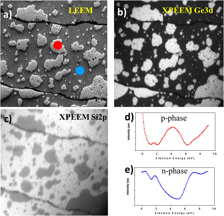
FIGURE 1. The real space characterization of the mixed phase in Ge-intercalated graphene. (A) A LEEM image (electron energy 3.5 eV) showing the islands of the p-doped phase in the sea of the n-doped phase. The height difference between p- and n-doped phases in the LEEM image is emphasized by moving the contrast aperture slightly away from the optimal position. (B) Ge3d XPEEM image of the same area as in (A). The white islands belong to the p-phase that has twice as much germanium compared to the n-phase. Photon energy hν = 100 eV and electron kinetic energy = 64 eV. (C) Si2p XPEEM image showing an extra attenuation of the Si2p photoelectrons going through the p-type islands. Photon energy hν = 150 eV and electron kinetic energy 45.2 eV. Field of view is 10 μm in all three images. (D,E) LEEM IV curves collected from areas marked by red and blue circles, respectively, in the LEEM image (A) displaying drastic difference in the reflectivity for p- and n-doped Ge-intercalated graphene.
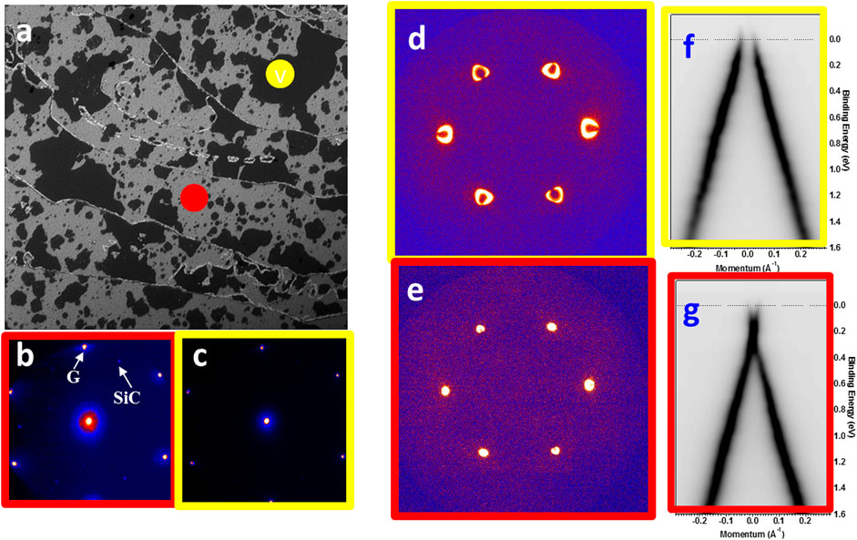
FIGURE 2. The reciprocal space (diffraction) characterization of the mixed-phase Ge-intercalated graphene. (A) A LEEM image of the surface: electron energy 6.5 eV and FoV = 25 μm. Yellow and red circles depict the areas where all diffraction data were collected (sampling area 1.5 μm). (B,C) Low-energy (50 eV) electron diffraction (LEED) from the n-doped and the p-doped graphene, respectively. (D,E) (Kx,Ky) photoelectron diffraction pattern acquired at Eb = 0.2 eV below the Fermi level from p-doped and n-doped areas, correspondingly. Photon energy 45 eV. (F,G) E(k) plot perpendicular to the G–K direction for the p-doped and n-doped phases, respectively.
Phase transition during the course of intercalation is not the only one in the SiC/Ge/graphene system. In the mixed phase, the ratio of p- and n-doped areas is governed by the annealing temperature of the intercalated p-phase (around 900°C). But the concrete surface morphology is the result of another phase transition which occurs at much lower temperatures (<500°C). In Figure 3, four still LEEM images are shown from the movie upon heating the sample (on yet another substrate) from room temperature up to 500°C (the full movie “heating.avi” is in the Supplementary information). No image drift correction has been applied to the whole set of data. The imaging electron energy is 4.5 eV which makes p-type doped graphene bright and n-type graphene dark (cf the LEEMIV curves in Figures 1D,E). At room temperature (Figure 3A), there are terraces which almost entirely p-doped and just slightly perforated by the n-phase (upper half of the LEEM image in Figure 3A). The terraces at the lower half of the LEEM image contain mainly n-doped graphene with some inclusions of the p-doped islands. Upon annealing a drastic change first happens at the upper terraces–around 300°C, the surface there looks entirely p-doped without any traces of the n-phase (Figure 3B). With a further increase in temperature (at around 450°C), the p-type islands in the bottom part of the image start to disappear (Figure 3C) until the whole terrace looks entirely n-doped at 500°C (Figure 3D). The most natural explanation for this phenomenon is the high mobility of germanium atoms at the interface at elevated temperatures. The amount of Ge atoms in the second layer makes the surface either p- or n-doped and when they are in motion, the whole surface will appear as purely p- (n-) doped even if the real germanium content on the terrace is slightly less than 2 ML (slightly more than 1 ML), respectively. The diffusion length depends on the temperature and that is why the transition is first visible on the predominantly p-doped terraces where germanium atoms diffuse over relatively short distances. With further heating, the diffusion length increases and the transition becomes visible on predominantly n-doped terraces. Now mobile Ge atoms in the second Ge layer belong to the whole terrace which appears as n-doped. It is important to note here that the sample used in the study has exceptionally large (≥5 mkm) terraces. As a result, there is a huge (several nanometers) step bunching on the surface and mobile germanium atoms make random movements within the same terrace bouncing off its borders. On cooling the phase transition is reversed but the transition temperature is much lower, as can be seen in Figure 4. Here are presented four still LEEM images which are taken from another movie (“cooling.avi,” Supplementary info) showing the reverse sequence of transitions with significant temperature hysteresis. The appearance of the p-phase islands on the n-type terraces starts to occur below 420°C (Figure 4B) and the transition is complete at 390°C. On the p-doped terraces, the n-phase first appears at 220°C (Figure 4C) which is about 100° below compared to the onset of the same transition on heating. The hysteresis curves for the transitions in both phases are presented in Figure 5. The Y-axis in the plots is the fraction of the appearing p- (n-) phase that was calculated and averaged from several areas in the LEEM images on both heating and cooling. The temperature hysteresis indicates that this phase transition is a first-order transition and the cooling rate is an important parameter for the final distribution of the p- and n-phases. But as seen in both movies, exactly the same spatial pattern is achieved after the heating and cooling cycle. The main reason for that is that the change in the cooling rate in the microscope is limited by the presence of the massive manipulator and objective. The time needed for heating the sample from room temperature up to 500°C is about 10 min and for cooling in the same temperature interval is even longer. But, in a different set-up, the tailoring of the final pattern in the mixed phase can be manipulated. It may be particularly important for applications utilizing controllable ballistic p–n junctions. Transmission of electrons through the p–n interface resembles the refraction with negative refraction index at the surface of metamaterials [19–21]. The group velocity of electrons in the conduction band Vc and in the valence band Vgv has the opposite sign (Figure 6A). As a result, the wave propagating in the n-region with the wave vector (Kx, Ky) will be transmitted into the p-region with the wave vector (Kx, -Ky) which makes the focusing properties of the n–p interface possible (Figure 6B) [22]. For an optimal focusing, two conditions should be met: 1) the width of the interface, w, should be quite sharp and 2) the doping level on both sides of the junction should not be much different [19]. For Ge-intercalated graphene, the doping level is very close for both phases: hole concentration is p = 4.1 × 1012 cm−2 for the p-phase and electron concentration n = 4.8 × 1012 cm−2 for the n-phase [13]. As for the transition width w, it should be less than electronic de Broglie wavelength, λd, which, in turn, depends on the doping level. For a doping of E = 0.2 eV (Figures 2F,G) λd follows from the relation λdE = hνF as λd≈17 nm. In reality, the transition width from p- to n-phase is on the scale of a couple of nanometers (ideally, atomically sharp) and w << λd. All this makes the mix phase of the Ge-intercalated graphene a promising candidate for the engineering of electronic lenses and creating repeated structures smaller than the electronic Fermi wavelength. One of the practical ideas would be to use a pattern of the mix phase at high temperatures (like those in Figures 3D, 4A) with a single boundary of several tens of microns. Having access to a fast cooling equipment, one can quench the substrate keeping the same distribution pattern at low temperatures. Using e-beam lithography, it should be possible to produce gateless devices on such substrates.
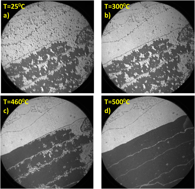
FIGURE 3. LEEM still images from the movie (“heating.avi”, Supplementary Material) showing low-temperature phase transition in the mix Ge-intercalated graphene upon heating. At room temperature (A), a mix phase is clearly seen, with different ratios of the p- and n-doped phases on different terraces. Ge atoms in the second layer start to move at around 300°C (B), and the upper terraces appear to be entirely p-doped. Upon further annealing at 460°C (C), the diffusion length increases, p-type islands start to disappear, and lower terraces appear to be entirely n-doped. At 500°C (D), the process is complete and Ge atoms in the second layer belong to the whole terrace in both phases. The electron energy is 4.5 eV, and FoV = 25 μm for all LEEM images.
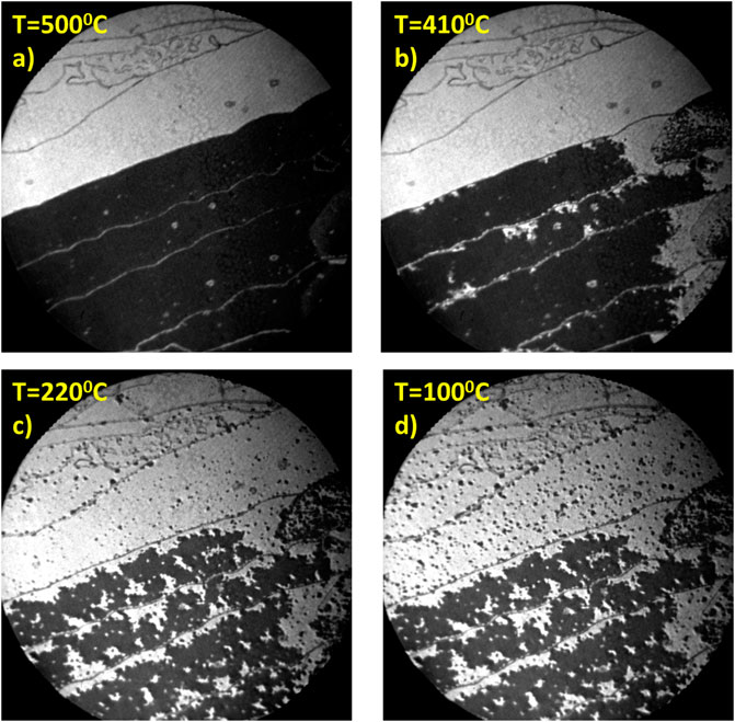
FIGURE 4. LEEM still images from another movie (“cooling.avi”, Supplementary information) showing low-temperature phase transition in the mix Ge-intercalated graphene on cooling. All transitions visible in Figure 3 are reversed but with a significant hysteresis. The p-type islands appears first on the n-type terraces at around 410°C (B), and the process completes at 370°C. N-type areas start to appear on the p-type terraces at much lower temperature, 220°C (C). The Ge atoms stop to move, and the phase transition is complete around 100°C (D). The electron energy is 4.5 eV, and FoV = 25 μm for all four LEEM images.
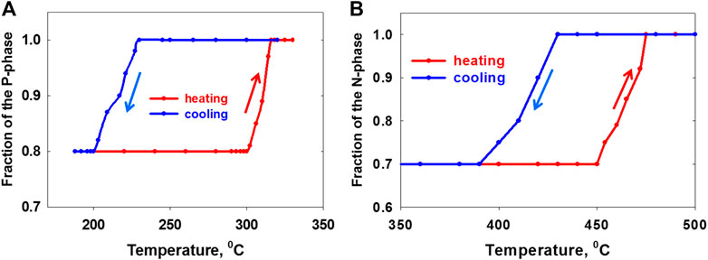
FIGURE 5. “Appeared” fraction of the p-phase (A) on the upper terraces and the n-phase (B) on the lower terraces upon heating (cooling). The plots demonstrate the first-order phase transition and significant temperature hysteresis. The corresponding fractions have been calculated and averaged over several areas (2 μm each) in the still LEEM images from the two movies.
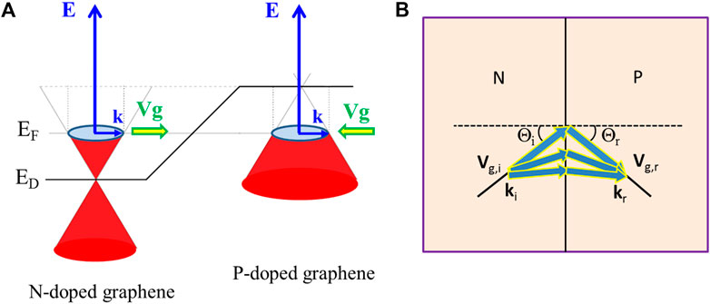
FIGURE 6. A) Energy diagram near a p–n junction in the Ge-intercalated graphene. Note the different signs of the electron group velocity on both sides of the junction. (B) A sketch of electron refraction at a sharp n–p boundary. The focusing effect occurs due to the negative refraction index at the sharp n–p interface.
Using spectroscopic photoemission and low-energy electron microscope with different imaging and spectroscopy modes, the mixed phase of germanium-intercalated graphene has been fully characterized. Upon Ge intercalation, the buffer layer, a quasi-freestanding graphene monolayer, forms and displays a moderate n- or p-doping depending on the amount of intercalated germanium. For the mixed phase, the second Ge-intercalated layer is incomplete and germanium atoms can move within a terrace at elevated temperatures (100°C < T < 500°C). This phase transition is the first-order transition with pronounced temperature hysteresis which implies that concrete realization of the p- and n-doped areas can be governed by the heating/cooling protocol. The enhanced Ge diffusion in the second layer can be suitable for tailoring ultrashort junction lengths so that pseudo-spin mismatch can be used in future electronic concepts. Due to the different sign of the electron group velocity on the p- and n-doped sides, the p–n boundary has a negative relative refractive index that can find possible applications in focusing electron optics.
The original contributions presented in the study are included in the article/Supplementary Material; further inquiries can be directed to the corresponding author.
AZ wrote the manuscript and made all experiments presented in the article.
The author declares that the research was conducted in the absence of any commercial or financial relationships that could be construed as a potential conflict of interest.
The handling editor declared a past co‐authorship with the author AZ.
The author thanks U. Starke and K. Emtsev who initiated Ge-intercalated project at the low-energy electron microscope at MAX-lab and provided wide terrace buffer layer graphene substrates for germanium intercalation. Another very good bunch of buffer layer samples used in the present study came from R. Yakimova. Support from the Swedish Foundation for Strategic Research (SSF), Grant Nos. RMA15–0024, is gratefully acknowledged.
The Supplementary Material for this article can be found online at: https://www.frontiersin.org/articles/10.3389/fphy.2021.641168/full#supplementary-material.
1. Berger C, Song Z, Li X, Wu X, Brown N, Naud C, et al. Electronic confinement and coherence in patterned epitaxial graphene. Science (2006) 312:1191. doi:10.1126/science.1125925
2. Johansson L, Xia C, Hassan J, Iakimov T, Zakharov A, Watcharinyanon S, et al. Is the registry between adjacent graphene layers grown on C-face SiC different compared to that on Si-face SiC. Crystals (2013) 3:1. doi:10.3390/cryst3010001
3. Starke U, Riedl C. Epitaxial graphene on SiC(0001) and SiC(0001): from surface reconstructions to carbon electronics. J Phys Condens Matter (2009) 21:134016. doi:10.1088/0953-8984/21/13/134016
4. Virojanadara C, Yakimova R, Zakharov AA, Johansson LI, Phys. D. Large homogeneous mono-/bi-layer graphene on 6H-SiC(0 0 0 1) and buffer layer elimination. J Phys D: Appl Phys (2010) 43:374010. doi:10.1088/0022-3727/43/37/374010
5. Emtsev KV, Bostwick A, Horn K, Jobst J, Kellogg GL, Ley L, et al. Towards wafer-size graphene layers by atmospheric pressure graphitization of silicon carbide. Nat Mater (2009) 8:203. doi:10.1038/nmat2382
6. Riedl C, Zakharov AA, Starke U. Precise in situ thickness analysis of epitaxial graphene layers on SiC(0001) using low-energy electron diffraction and angle resolved ultraviolet photoelectron spectroscopy. Appl Phys Lett (2008) 93:033106. doi:10.1063/1.2960341
7. Mattausch A, Pankratov O. Ab initio study of Graphene on SiC. Phys Rev Lett (2007) 99:076802. doi:10.1103/physrevlett.99.076802
8. Cavallucci T, Tozzini V. Intrinsic structural and electronic properties of the Buffer Layer on Silicon Carbide unraveled by Density Functional Theory. Scientific Rep (2018) 8:13097. doi:10.1038/s41598-018-31490-7
9. Emtsev K, Speck F, Seyller T, Ley L, Riley J. Interaction, growth, and ordering of epitaxial graphene on SiC{0001} surfaces: A comparative photoelectron spectroscopy study. Phys Rev (2008) B77:155303.
10. Riedl C, Coletti C, Iwasaki T, Zakharov AA, Starke U. Quasi-free-standing epitaxial Graphene on SiC obtained by hydrogen intercalation. Phys Rev Lett (2009) 103:246804. doi:10.1103/physrevlett.103.246804
11. Giertz I, Suzuki T, Weitz R, Lee D, Krauss B, Riedl C, et al. Electronic decoupling of an epitaxial graphene monolayer by gold intercalation. Phys Rev (2010) B81:235408.
12. Forti S, Link S, Stohr A, Niu Y, Zakharov AA, Coletti C, et al. Semiconductor to metal transition in two dimensional gold and its van der Waals heterostack with graphene. Nat Commun (2020) 11:2236. doi:10.1038/s41467-020-15683-1
13. Emtsev KV, Zakharov AA, Coletti C, Forti S, Starke U. Ambipolar doping in quasifree epitaxial graphene on SiC(0001) controlled by Ge intercalation. Phys Rev (2011) B84:125423.
14. Baringhaus J, Stöhr A, Forti S, Krasnikov SA, Zakharov AA, Starke U, et al. Bipolar gating of epitaxial graphene by intercalation of Ge. Appl Phys Lett (2014) 104:261602. doi:10.1063/1.4886411
15. Kim H, Dugerjav O, Lkhagvasuren A, Seo JM. Origin of ambipolar graphene doping induced by the ordered Ge film intercalated on SiC(0001). Carbon (2016) 108:154. doi:10.1016/j.carbon.2016.07.010
16. Yakimova R, Virojanadara C, Gogova D, Syväjärvi M, Siche D, Larsson K, et al. Analysis of the formation conditions for large area epitaxial graphene on SiC substrates. Msf (2010) 645-648:565. doi:10.4028/www.scientific.net/msf.645-648.565
17.Eremitenweg. Gauting, Germany. Available at: https://www.tvips.com/.
18. Zakharov AA, Virojanadara C, Watcharinyanon S, Yakimova R, Johansson L. Nanoscale 3-D (E, kx, ky) band structure imaging on graphene and intercalated graphene. IBM J Res Dev 55, no4, paper 6 (2011).
19. Veselago VG. The electrodynamics of substances with simultaneously negative values of ε and μ. Sov Phys Usp (1968) 10:509. doi:10.1070/pu1968v010n04abeh003699
20. Cheianov VV, Fal'ko V, Altshuler BL. The focusing of electron flow and a veselago lens in graphene p-n junctions. Science (2007) 315:1252. doi:10.1126/science.1138020
21. Lee G-H, Park G-H, Lee H-J. Observation of negative refraction of Dirac fermions in graphene. Nat Phys (2015) 11:925. doi:10.1038/nphys3460
Keywords: Graphene, Ge intercalation, p–n junctions, electron focusing, LEEM, XPEEM
Citation: Zakharov AA (2021) Ambipolar Behavior of Ge-Intercalated Graphene: Interfacial Dynamics and Possible Applications. Front. Phys. 9:641168. doi: 10.3389/fphy.2021.641168
Received: 13 December 2020; Accepted: 09 February 2021;
Published: 13 April 2021.
Edited by:
Stiven Forti, Italian Institute of Technology, ItalyReviewed by:
Marko Kralj, Institute of Physics, CroatiaCopyright © 2021 Zakharov. This is an open-access article distributed under the terms of the Creative Commons Attribution License (CC BY). The use, distribution or reproduction in other forums is permitted, provided the original author(s) and the copyright owner(s) are credited and that the original publication in this journal is cited, in accordance with accepted academic practice. No use, distribution or reproduction is permitted which does not comply with these terms.
*Correspondence: A. A. Zakharov, QWxleGVpLlpha2hhcm92QG1heGl2Lmx1LnNl
Disclaimer: All claims expressed in this article are solely those of the authors and do not necessarily represent those of their affiliated organizations, or those of the publisher, the editors and the reviewers. Any product that may be evaluated in this article or claim that may be made by its manufacturer is not guaranteed or endorsed by the publisher.
Research integrity at Frontiers
Learn more about the work of our research integrity team to safeguard the quality of each article we publish.