 Cinzia Da Via1,2*
 Paolo Petagna3
 Giulia Romagnoli3Desiree Hellenschmidt3Francisca Munoz-Sanchez1Nicholas Dann1
- 1Physics and Astronomy Department, The University of Manchester, Manchester, United Kingdom
- 2Physics and Astronomy Department, Stony Brook University, Stony Brook, NY, United States
- 3European Council for Nuclear Research, CERN, Geneva, Switzerland
The growing demand for miniaturized radiation-tolerant detection systems with fast responses and high-power budgets has increased the necessity for smart and efficient cooling solutions. Several groups have been successfully implementing silicon microfabrication to process superficial microchannels to circulate coolants, in particular, in high-energy physics experiments, where the combination of low material budget to reduce noise generated by multiple scattering events and high radiation fluences is required. In this study, we report tests performed on an 885-µm–thick vertically integrated system. The system consists of a layer of microfabricated silicon channels for temperature management integrated to radiation-tolerant microfabricated 3D sensors, with electrodes penetrating perpendicularly to the silicon bulk, bump-bonded to an ATLAS FE-I4 pixel readout chip of 100 µm thickness, 2 × 2 cm2, and 26,880 pixels (each measuring 250 × 50 μm2). The system’s electrical and temperature characterization under CO2 cooling as well as the response to minimum ionizing particles from radioactive sources and particle beams before and after 2.8 ×10¹⁵ neq cm−2 proton irradiation will be discussed.
Introduction
Microelectromechanical systems (MEMSs) made their appearance in the late 1980s and have been steadily growing their applications in several fields, ranging from car industry, mobile phones, fundamental science, space applications, and more [1–4]. The key asset of MEMS fabrication is the possibility of processing miniaturized tailor etching features inside high purity silicon and therefore uses contemporarily its semiconducting, electrical, and mechanical properties In fundamental science research, microfabrication was used in the 1990s to process 3D silicon sensors [5]. In 3D sensors, electrodes are deeply etched fully or partially through the silicon bulk to produce electrodes of p–n diodes. When a particle penetrates the silicon active volume to be detected, it loses energy. While the “ionizing” energy that goes into the creation of electron–hole pairs leads to fully reversible processes that leave no damage, “non-ionizing” energy transfers to the atoms of silicon crystal lead to irreversible changes. The latter depends on the type and energy of the particles. The most fundamental type of non-ionizing damage is the creation of a “Frenkel defect,” where an atom is knocked off its site into an interstitial position, leaving a vacancy behind. The energy transfer threshold for this process is 25 eV. For higher energy transfer, a primary knock-on atom can generate clusters of crystalline damage along its path. The vacancies and interstitials can migrate even at low temperatures. They would form stable defects when they combine with impurities, such as carbon and oxygen, and dopants, such as phosphorus and boron. Such defects act as carrier traps and, if they are near the middle of the bandgap, as efficient generation centers. The consequences of the presence of silicon radiation damage are leakage current increase and loss of signal due to the reduced carrier lifetime and can be mitigated by working at saturated drift velocity. The benefits of a complex design such as 3D became evident immediately: The generated signal is faster, and the sensor can tolerate a far greater amount of non-ionizing energy transfer compared to a traditional planar geometry because of the stronger and electric field throughout the bulk [6].
Microfabricated channels have also shown to be interesting for circulation of cooling fluids. Attempts in this respect have been successful in power managing microprocessors and latter in high energy physics experiments at the CERN Large Hadron Collider’s experiments aiming at pushing research discoveries by precision measurements of the particles’ trajectories [7–10]. The ATLAS experiment used 3D silicon sensors for the first time in the Insertable B-Layer (IBL), which was installed in 2012 and successfully collected data, together with innovative planar sensors since 2014 [11]. The inner tracker of ATLAS will undergo a full replacement in 2026 to prepare the experiment for the accelerator’s luminosity increase, which will allow accessing processes too rare to be seen with the current statistics. The further increase of luminosity and electronics performance, associated with the increased radiation exposure, will increase the power dissipation budget of the full system even with a low-power 65-nm technology chip such as the future RD53 [12]. This is the main motivation for exploring approaches, which demonstrated their validity in experiments, such as NA62, ALICE, and LHCb also to the larger, and more challenging, environments of experiments such as ATLAS.
The 3D Vertically Integrated Module
A sketch of the 3D vertically integrated module (not to scale) can be seen in Figure 1. The 885-µm thick vertically integrated stack is composed, from the top, by a 285-µm thick double-sided 3D silicon module, fabricated by CNM [13] using the IBL design with 75-µm inter electrode spacing and a full depletion bias voltage of 10 V, and bump-bonded to a 100-µm thick FE-I4A pixel readout electronics [14]. At the bottom, the sensor-electronics assembly is glued using a two-component Masterbond EP37-3FLFAO [15] to a custom-made 500-µm thick silicon-silicon direct-bonding (made at CSEM [16]) microchannel cooling device designed by the CERN PH-DT group and fabricated by the same group at the EPFL CMi [17] cleanroom.
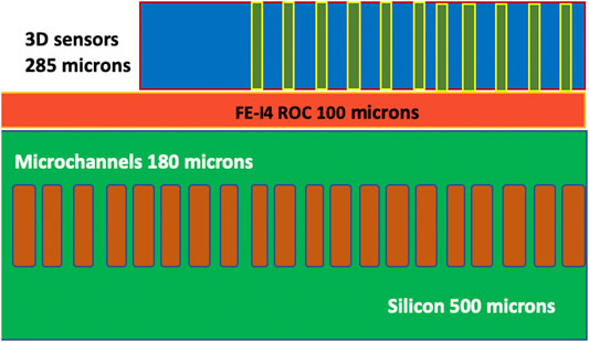
FIGURE 1. Sketch of the vertically integrated 3D system with 285-µm-thick double-sided partially through 3D sensors (top), 100-µm-thick FE-I4A ATLAS pixel readout electronics (middle), and 500-µm-thick silicon-etched microchannels for thermal management (bottom). The distance from the microchannels to the electronic chip is 120 µm; the channels’ depth is 180 µm. The total thickness of the system including the sensor and electronics is 885 µm.
A plan of the 2 × 4-cm2 microchannel device, conceived for operation with evaporative CO2 flows, is represented in Figure 2. The overall scheme is the same used for a device successfully adopted in a previous study [18]: Parallel channels are fed through restrictions from a single inlet manifold and have a “C-shape” to reach a common outlet manifold located on the same side of the inlet one. This arrangement simplifies the implementation of the hydraulic connections and allows for simple and relatively uniform fluid distribution underneath the chip area. In order to ensure a uniform distribution, CO2 enters the restrictions slightly sub-cooled (i.e., in the liquid phase) and is brought to saturation conditions at the entrance of each channel by the pressure drop induced by the restrictions. As shown in [18], this arrangement favors an immediate onset of nucleate boiling at the beginning of each channel. The device is operated with very low vapor quality at the exit; therefore, the difference in total pressure drop between channels caused by the simple “C-shape” geometry has negligible effects on the thermal uniformity. In this design, each of the 35 microchannels has dimensions 50 × 180 µm2 and is separated from the next one by 200 µm wide walls. With respect to the geometry previously studied, the number of parallel channels has been increased and a larger aspect ratio has been adopted for their cross section, favoring a larger heat transfer coefficient [19].
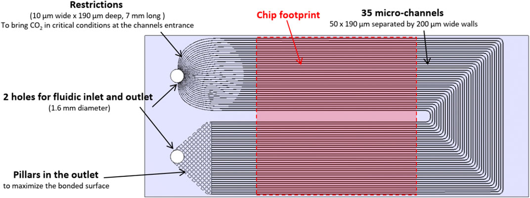
FIGURE 2. Plan of the 2 × 4-cm2 microchannel device, conceived for operation with evaporative CO2 flows showing the 35 parallel channels, 50 × 190 µm squared, separated by 200 µm wide walls, which are fed through restrictions from a single inlet manifold visible on the top left. They have a “C-shape” to reach a common outlet manifold located on the same side of the inlet one and visible on the bottom left. Both inlet and outlet holes have a 16 mm diameter.
Both 3D sensors with n+ and p+ electrodes penetrating partially from the front and back side wafer’s surfaces and microchannels for thermal management were fabricated using deep reactive ion etching technology to generate deep cylindrical holes in the former and superficial grooves in the latter [20].
After integration, the vertical assembly was mounted on a dedicated Printed Circuit Board (PCB) fabricated in the Physics Institute at Bonn University for the FE-I4 electronics readout followed by wire bonding at the CERN PH-DT bonding lab facility.
A 3D printed Acrylonitrile Butadiene Styrene (ABS) support was manufactured to host the PCB and a lateral support for the bended inlet and outlet stainless-steel tubes used to carry the CO2 to the microchannels, as can be seen in Figure 3.
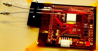
FIGURE 3. Picture of the 3D printed black ABS support hosting the FE-I4 compatible PCB, designed at Bonn University, and the support for the stainless-steel inlet–outlet pipes. The 4 cm2 vertically integrated 3D sensor is visible in the center (white square). On the left, the copper-plated Kovar connectors are connected (soldered) to the microchannel chip.
On the left of the 4 cm2 module, the Kovar connectors [21] laser soldered to the copper-coated stainless-steel tubes are visible. A characteristic feature of two-phase CO2 circuits is their relatively high pressure, typically reaching levels in the order of 60 bars when operated at room temperature. One of the main concerns for any hydraulic circuit subject to high pressure is the mechanical resistance of the connector. Pressure tests performed on the Kovar connectors demonstrated reliability in excess to 80 bars, thus providing a comfortable safety margin with respect to the highest expected pressure in operation.
Experimental Results
Thermal Tests
To assess the successful performance of the microchannel cooling structure, tests were carried out using the Transportable Refrigeration Apparatus for CO2 Investigation (TRACI) system [22]. To protect the module from freezing, the board was housed in a vessel equipped with a vacuum pump that provides a vacuum level of 10–3 bar. A flange with electrical feedthroughs was used to carry in the input bias voltages and out the electrical signals, as can be seen in Figure 4. The temperature in different points of the boards and the module was measured using PT100 thermal sensors. A map of the sensors’ position can be seen in Figure 5A on the board and (B) on the microchannel chip.
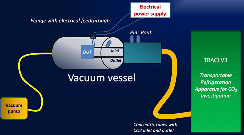
FIGURE 4. Sketch of the refrigeration system used to test the vertically integrated module. A vacuum pumped vessel is used to host the module and is connected to TRACI with CO2 inlet and outlet tubes. A flange with electrical feedthroughs allows the applications of bias voltages and the extraction of electrical signals from the vessel.
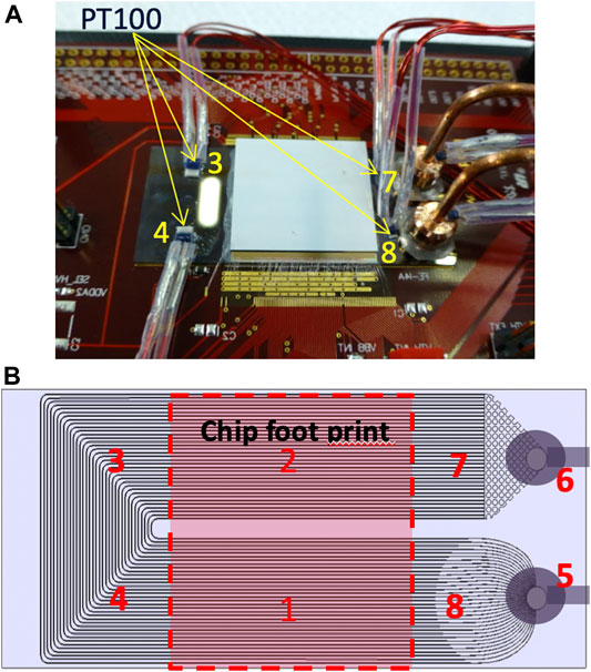
FIGURE 5. (A) Position of the FP100 temperature sensors on the PCB board. (B) Numbered position of the PT100 thermal sensors on the microchannel chip. Sensors 1 and 2 were glued on the back of the module and were therefore about 400 µm away from the channel themselves.
As can be seen from Figure 5B, the silicon microchannels, custom designed for the FE-I4 sensor chip, have a “C” shape and larger dimensions than the 4 cm2 FE-I4 footprint to allow the CO2 evaporation to take place in the channels before reaching the chip itself. The FE-I4 chip was positioned at the center of the microchannels as indicated by the red footprint in the figure, while point 5 corresponds to the coolant “inlet” and point 6 indicates the “outlet.” Due to limitations of the setup, it was impossible to set the CO2 flow during the cooling process to a lower value than 0.5 g/s: This is a large overflow with respect to the power dissipated by the chip, producing a very low vapor quality at the outlet of the cooling device, below 1%. It is worth noticing that a large vapor quality would produce a higher heat transfer coefficient and therefore a more effective thermal management. The performance recorded for the cooling device in the present tests is therefore suboptimal and could be enhanced by a finer regulation of the mass flow rate. Further details on the CO2 microchannel cooling evaporative functionality can be found in References [10, 23].
The 3D sensor’s current–voltage (IV) curves at different temperatures are visible in Figure 6A. During the IV measurements, the FE-I4 chip was switched off. A bias voltage interval between −50 and 0 V was chosen to check the sensor robustness. A negative voltage of −15 V is necessary for the junction full depletion bias, and no breakdown is observed well above over depletion. The accuracy of the PT100 measurements was evaluated at ±0.1°C. The temperature difference between the TRACI setpoint and the CO2 temperature measured by the PT100 at point five was recorded to be in average 2°C. Each temperature recorded on the microchannels by the PT100 sensors was an average of 10 measurements.
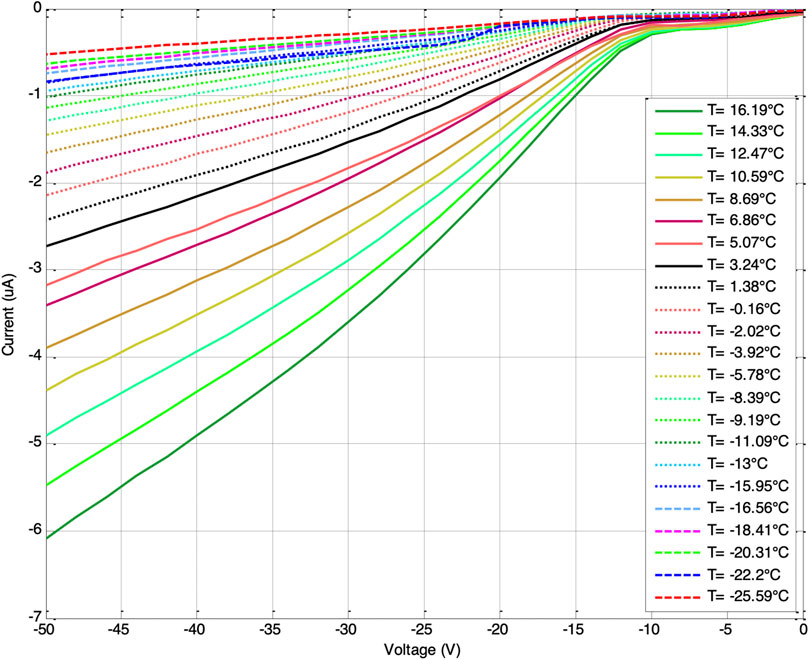
FIGURE 6. Current–voltage curves at different temperatures with the FE-I4 chip switched off. Each temperature was measured by PT100 temperature sensors and is an average of 10 measurements.
The temperature reproducibility was checked by measuring repeatedly the IV at three different temperatures and by scanning the temperature ascending and descending at a fixed bias voltage of 30 V. The two plots are shown in Figures 7A,B. A variance of 0.1 uA in the current curves at the same temperature and fixed bias voltage is visible on both curves and is mainly due to ramp-up/ramp-down hysteresis. The intent of these tests was to demonstrate that the sensor’s leakage current could eventually be used to measure its temperature directly in case a sensor could not be glued on its surface.
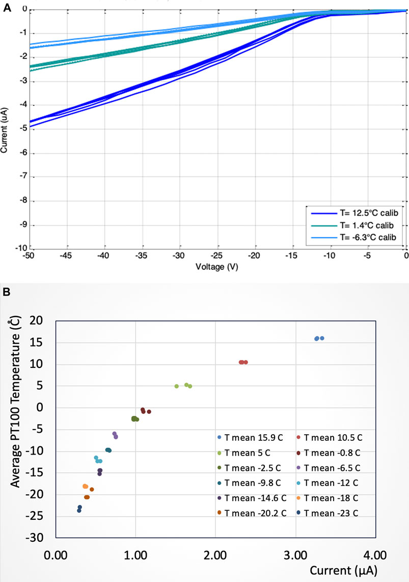
FIGURE 7. (A) Current–voltage (IV) curves repeated at three different temperatures to check the reproducibility of the temperature verified by repeatedly measuring the IV curve at three different temperatures and measuring the temperature–current relationship by varying the temperature in increasing and decreasing directions at a fixed bias voltage of 30 V (B).
A useful parameter to assess the performance of a specific thermal management configuration is the so-called Thermal Figure of Merit (TFoM). This is conventionally defined as the temperature difference between the refrigerant and the sensor under operational conditions divided by the applied power density [24]. The TFoM represents the capability of the coolant to remove the temperature generated by a certain dissipated power per unit area and can be interpreted as a measure of the global thermal resistance of a complete detector module configuration: the smaller its value, the lower the sensor’s temperature in operation for fixed power dissipation and refrigerant temperature will be. As a reference, the TFoM of the ATLAS Inner Detector (ID) laboratory study of the Insertable B-Layer (IBL) evaporative CO2 configuration has been evaluated at 13 Kcm2/W at −20°C [25], which is the lowest value for cold silicon detectors in operation at LHC.
In the present work, as it was not possible to install a PT100 directly on the sensor’s surface, the reference temperature was estimated from the temperatures recorded by all the installed PT100 during the leakage current tests, performed at different temperatures with the electronic chip switched off and switched on. The assembly was modeled in the FEA software, and simple conductive thermal calculations were conducted, using the measured CO2 temperature as the boundary condition in the channels and assuming an additional 10% power dissipation in the sensor on top of the one from the chip, as it had been already heavily irradiated prior to its coupling with the microchannel device. As the leakage current tests were executed under vacuum, purely adiabatic conditions were considered for the calculations. The model was calibrated with respect to the temperature measurements from the six PT100 installed on the assembly and provided a reasonably accurate estimate of the sensor temperature. The typical temperature difference DT between the CO2 and the sensor was estimated to be about 1.5°C for CO2 temperatures in the order of −20°C. With the power dissipated by the FE-I4 electronics of 1.5 W over its 4 cm2 area, the TFoM becomes
It should be noted that the additional dissipation in the sensor was not taken into account in the evaluation of the TFoM, which should therefore be considered as a slightly conservative estimate The value of 4 Kcm2/W calculated compares well with the direct measurements of a TFoM slightly larger than 3 Kcm2/W gathered for the very similar multi-microchannel device studied in [18].
Minimum Ionizing Particle Tests
The response of the module to minimum ionizing particles was tested using a 90Sr beta source and, after irradiation, a beam test at the CERN SPS beamline facility. The occupancy and Time over Threshold (ToT) from the beta source can be seen in Figures 8A,B, respectively, showing the correct functionality of the sensor and the 100 microns thick FE-I4 electronic chip. For these tests, the sensor was biased at 20 V at room temperature. For this test, the source was collimated. The columns 38–39 in the occupancy plot in Figure 8A are not connected, while the peak at ToT = 14 in Figure 8B is a feature of the FE-I4 readout chip, which uses bin 14 as overflow for all the signal charges that are over the maximum range. To further test the cooling robustness of the vertically integrated system, the module was exposed to a 300 GeV pion beam at the CERN SPC H6 beamline after being irradiated to 2.8 × 10¹⁵ neqcm−2 at the CERN proton irradiation facility [26]. The TRACI was transported to the beamline, and a 3D printed ABS box filled with insulating foam was used to host the board during the test. The board was aligned with the ATLAS FE-I4 pixel telescope [27]. The module was cooled to −22°C and biased at 200 V, while nitrogen gas was constantly blown on the module to prevent icing. Pictures of the beamline with the TRACI and the board inserted in the 3D printed box are shown in Figure 9. The correct functionality of the module and the cooling system can be appreciated by the data reported in Figure 10A, which are showing a linear correlation between the X coordinate of the 3D vertical module and the X coordinate of the first ATLAS FE-I4 pixel telescope’s plane, and Figure 10B shows partially the beam shape. After irradiation, the noise would be dominant and such data would not be visible without proper cooling and correct functionality of the module.
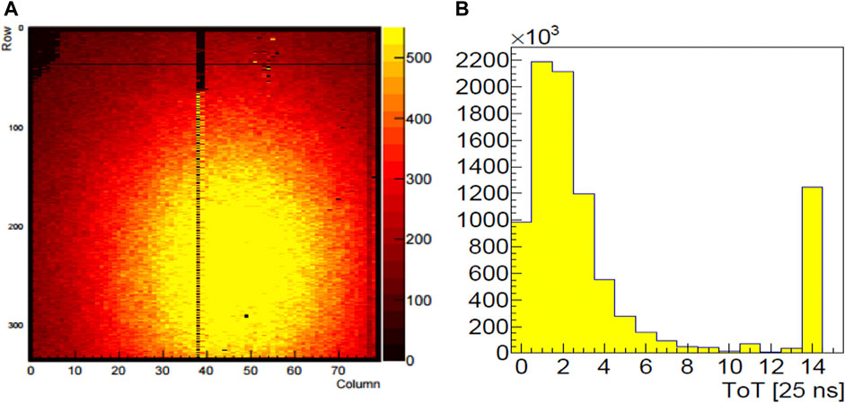
FIGURE 8. Response to the 90Sr beta radioactive source before irradiation at room temperature. (A) Pixel occupancy and (B) time over threshold spectrum. The counts at channel 14 is a feature of the FE-I4 readout chip, which uses bin 14 as overflow for all the signal charges that are over the maximum range.
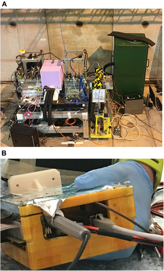
FIGURE 9. Picture of the test beam setup at the CERN SPS H6 beamline. (A) ATLAS Fe-I4 telescope on the left and the TRACI cooling plant on the right. (B) The 3D printed cooling box hosting the vertically integrated system showing details of the electrical cables.
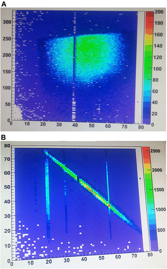
FIGURE 10. 3D sensor response to the 300 GeV pion beam after irradiation at −22°C. (A) Beam profile where the sharp transition above 250 in the vertical direction is due to bean misalignment and (B) correlation curve of the x coordinate of the DUT and the one of the x coordinate of the first FE-I4 telescope plane.
After collecting the beam profile and the correlation curves between the 3D sensor’s module and the telescope, the beam was lost and the test beam ended. The module was transported back to the laboratory where it was impossible to revive it. It is believed that irreversible damage happened during the dismantling and transportation of the module.
Conclusion
An 883-µm-thick vertically integrated system consisting of a radiation-hard 3D silicon sensor, a 100-µm-thick FE-I4 pixel electronic chip, and a 500-µm-thick silicon microchannel cooling module for thermal management was successfully tested with radioactive sources and 300 GeV pion particle beam after 2.8 × 10¹⁵ neqcm−2 proton irradiation while cooled with evaporative CO2. Thermal tests proved the superior cooling power of a silicon microchannel device operated with boiling CO2. The thermal figure of merit, defined as the temperature difference between the refrigerant and the sensor under operational conditions divided by the applied power density, was evaluated to be 4 Kcm/W. This value should be compared with 13 Kcm/W obtained with the same chip in the ATLAS IBL configuration with CO2 boiling in a standard metal pipe.
Technological issues must clearly be solved before such advanced cooling devices may find direct applications in 4π solid angle experiments, mainly linked to the cost and reliability of the multiple hydraulic connections involved. However, future runs at HL. HLC might require lower operation temperatures for the innermost pixel layers: microchannel devices, providing a factor of 3–4 reduction in the temperature difference between the sensor and refrigerant, might be considered in such cases as a viable alternative to the adoption of exotic ultra-low–temperature cooling systems.
Data Availability Statement
The raw data supporting the conclusions of this article will be made available by the authors, without undue reservation.
Author Contributions
CDV procured the components lead the assembly of the integrated system and wrote the study, GR designed, processed, and tested the microchannels, DH performed the thermal tests, FMS and ND performed the particle beam tests and PP supervised the thermal testing and contributed to the description of the thermal results.
Conflict of Interest
The authors declare that the research was conducted in the absence of any commercial or financial relationships that could be construed as a potential conflict of interest.
Acknowledgments
We would like to thank the colleagues at Bonn University for providing the PCB support board, Federico Ravotti, for organizing and performing the irradiation of the module, the CERN personnel at the bonding lab, Marco Battaglia for organizing the test beam, Malte Backhaus for his help with the FE-I4 readout system, and Giulio Pellegrini for providing the 3D sensor. We also thank Julian Firestone and Mike Perry at the University of Manchester for helping with the 3D printed test beam cooling box and their continuous support.
References
1. Bao M, Wang W. Future of microelectromechanical systems (MEMS). Sensors Actuators A: Phys Vol (1996) 56(1–2):135–41. doi:10.1016/0924-4247(96)01274-5
2. Petersen K, Digest T, MEMS: what lies ahead. In: 8th Internatonal Conference on Solid-State Sensors and Actuators/Eurosensors IX; 25–29 June; Stockholm, Sweden (1995). p. 894–7. doi:10.1109/SENSOR.1995.717377
3. Kraft M, Neil M. White; MEMS for automotive and aerospace applications. Sawston, Cambridge: Woodhead Publishing (2013). p. 978.
4. Potekhina A, Wang C. Review of electrothermal actuators and applications. Actuators (2019) 8:69. doi:10.3390/act8040069
5. Da Via C, Boscardin M, Darbo G, Fleta C, Gemme C, et al. 3D silicon sensors: design, large area production and quality assurance for the ATLAS IBL pixel detector upgrade. Nucl Instr Methods Phys Res Sect A Acc Spectrom Detect Assoc Equip (2012) 694:321. doi:10.1016/j.nima.2012.07.058
6. Mendicino R, Boscardin M, Dalla Betta G-F. Characterization of FBK small-pitch 3D diodes after neutron irradiation up to 3.5 × 10 16 n eq cm−2. Berlin: Springer (2020). doi:10.1088/1748-0221/14/01/C01005
7. Jackson BM, John RT, Bruno M. Cooling of microprocessors with micro-evaporation: a novel two-phase cooling cycle. Int J Refrig (2010) 33:1264–76. doi:10.1016/j.ijrefrig.2010.06.008
8. Romagnoli G, Feito DA, Brunel B, Catinaccio A, Degrange J, Mapelli A, et al. Silicon micro-fluidic cooling for NA62 GTK pixel detectors. Microelectronic Eng (2015) 145:133–7. doi:10.1016/j.mee.2015.04.006
9. Mapelli A, Petagna P, Renaud P. Microchannel cooling for high-energy physics particle detectors and electronics. 13th InterSociety Conference on Thermal and Thermomechanical Phenomena in Electronic Systems; 30 May–1 June 2012; San Diego, CA (2012). p. 677–83. doi:10.1109/ITHERM.2012.6231493
10. Nomerotski A, Buytarta J, Collinsa P, Dumpsa R, Greeningb E, John M, et al. Evaporative Co2 cooling using microchannels etched in silicon for the future LHCb vertex detector. Geneve 23, Switzerland: JINST 8 P04004 (2013). doi:10.1088/1748-0221/8/04/P04004
11.The ATLAS IBL Collaboration. Production and integration of the ATLAS insertable B-layer. JINST (2018) 13(05):T05008. doi:10.1088/1748-0221/13/05/T05008
12. Conti E, Barbero M, Fougeron D, Godiot S, Menouni M, Pangaud P, et al. The RD53 collaboration, development of a large pixel chip demonstrator in RD53 for ATLAS and CMS upgrades “POSTWEPP-17” 005. Berlin: Springer (2018).
13.Centro nacional de Microelectrónica (CSIC). Barcelona, Spain (2019). Available from: https://www.imb-cnm.csic.es/en.
14. Backhaus M. Characterization of the FE-I4b pixel readout chip production run for the ATLAS insertable b-layer upgrade. J Instrumen (2013) 8(03):C03013. doi:10.1088/1748-0221/8/03/C03013
16.Centre Suisse d'Electronique et de Microtechnique (CSEM). Neuchâtel, Switzerland (2018). Available from: https://www.csem.ch/.
17.Center of MicroNanotechnology—CMi, EPFL. Lausanne (2020). Available from: https://www.epfl.ch/research/facilities/cmi/.
18. Hellenschmidt D., Bombenc M, Saadanya B, Boscardind M, Crivellarid M, Ronchin S, et al. New insights on boiling carbon dioxide flow in mini- and microchannels for optimal silicon detector cooling. NIMA (2020) 958:162535. doi:10.1016/j.nima.2019.162535
19. Chen L, Hou Y, Li X, Xiao R, Lv K, Yang X. Flow boiling of low-pressure water in microchannels of large aspect ratio. Energies (2020) 13:2689. doi:10.3390/en13112689
20. Marty F, Rousseaua L, Xiao R, Merciera B, Francaisa B, Mitab Y, et al. Advanced etching of silicon based on deep reactive ion etching for silicon high aspect ratio microstructures and three-dimensional micro- and nanostructures. Microelectronics J (2005) 36:673–7. doi:10.1016/j.mejo.2005.04.039
22. Verlaat B, Zwalinski L, Dumps R. TRACI, a multipurpose CO2 cooling system for R&D. In: 10th IIF/IIR Gustav Lorentzen Conference on Natural Working Fluids; Delft, The Netherlands (2012).
23. Thome JR, Ribatski G. State-of-the-art of two-phase ow and ow boiling heat transfer and pressure drop of CO2 in macro- and microchannels. Int J Refrig (2005) 28:1149. doi:10.1016/j.ijrefrig.2005.07.005
24. Petagna P, Verlaat B, Francescon A. Two-phase thermal management of silicon detectors for high energy physics. In: JR Thome, editor. Encyclopedia of two-phase heat transfer and flow III. Singapore: World Scientic (2018). p. 335–412. doi:10.1142/9789813229471_0005
25. Capeans M, Darbo G, Einsweiller K, Elsing M, Flick T, Garcia-Sciveres M, et al. ATLAS collaboration, ATLAS insertable B-layer technical design report. Madrid, Spain: CERN-LHCC-2010-013 (2010).
Keywords: 3D sensors, micro-channel cooling, CO2, vertical integration, pixel detectors, radiation hardness, LHC upgrade
Citation: Da Via C, Petagna P, Romagnoli G, Hellenschmidt D, Munoz-Sanchez F and Dann N (2021) Vertically Integrated System with Microfabricated 3D Sensors and CO2 Microchannel Cooling. Front. Phys. 9:633970. doi: 10.3389/fphy.2021.633970
Received: 26 November 2020; Accepted: 02 February 2021;
Published: 22 April 2021.
Edited by:
Angela Kok, Sintef Digital, NorwayReviewed by:
Giovanni Darbo, National Institute of Nuclear Physics of Genoa, ItalyLeonello Servoli, Istituto Nazionale di Fisica Nucleare di Perugia, Italy
Copyright © 2021 Da Via, Petagna, Romagnoli, Hellenschmidt, Munoz-Sanchez and Dann. This is an open-access article distributed under the terms of the Creative Commons Attribution License (CC BY). The use, distribution or reproduction in other forums is permitted, provided the original author(s) and the copyright owner(s) are credited and that the original publication in this journal is cited, in accordance with accepted academic practice. No use, distribution or reproduction is permitted which does not comply with these terms.
*Correspondence: Cinzia Da Via, Y2luemlhLmRhdmlhQG1hbmNoZXN0ZXIuYWMudWs=