- Instrumentation Division, Brookhaven National Laboratory, Upton, NY, United States
Low-Gain Avalanche Diodes are a recently-developed class of silicon sensors. Characterized by an internal moderate gain that enhances the signal amplitude and if built on thin silicon substrates of a few tens of microns, they feature fast signals and exhibit excellent timing performance. Thanks to their fast timing they are planned to be exploited in timing detectors in High-Energy Physics experiments, for example for the upgrades of the ATLAS and CMS detectors at the High Luminosity Large Hadron Collider (HL-LHC) at CERN. However, to achieve a spatially uniform multiplication a large pixel pitch is needed, preventing a fine spatial resolution. To overcome this limitation, the AC-coupled LGAD approach was introduced. In this type of device, metal electrodes are placed over an insulator at a fine pitch, and signals are capacitively induced on these electrodes. The fabrication technology is similar for the two LGAD families, although a fine tuning of a few process parameters needs to be carefully studied. Other R&D efforts towards detectors that can simultaneously provide good time and spatial resolution, based on the LGAD concept, are under way. These efforts aim also to mitigate the loss of performance at high irradiation fluences due to the acceptor removal within the gain layer. In this paper we describe the main points in the fabrication of LGADs and AC-LGADs in a clean-room. We also discuss novel efforts carried on related topics.
1 Introduction
Detection of minimum ionizing particles (mips) is easily achieved with silicon-based detectors. In fact, High Energy Physics (HEP) experiments started using silicon strip detectors back in 1980 [1]. The amount of charge released by a mip is about 80 electron/hole pairs per micron of silicon traversed which gives origin to a fair signal that can easily be detected by modern read-out electronics. Even in the case of thin sensors, which may be preferred to limit both the applied voltage (especially after irradiation) and the Coulomb scattering, which deliver less charge while adding capacitance at the read-out node, such detection does not constitute an issue. For example the ATLAS [2] and CMS [3] experiments at CERN count millions of channels, and their innermost layers are populated with thin silicon sensors that undergo a severe irradiation. The front-end read-out electronics is typically based on a charge sensitive amplifier at the input stage followed by some filtering or shaping stage for noise reduction. Shaping times of a few hundreds of nanoseconds are typical; they are not chosen to maximize the Signal-to-Noise ratio (S/N) but to cope with the high rate of events expected.
However, in the future operation of the above mentioned experiments, an increase in luminosity is foreseen and multiple interactions are expected per bunch crossing. To distinguish tracks belonging to different vertexes, the proposed solution is to add timing information to the tracks (in the order of tens of picoseconds) because the interactions are separated in time by that amount. If we are able to read-out at the necessary speed, we can disentangle multiple primary and secondary vertexes, reduce ghost tracks, and generally ease the reconstruction [4]. Thus far, this cannot be achieved with the standard silicon detectors used.
A new silicon detector, which has been under development for a few years, has been chosen for this application due to its timing performance [5, 6]. It is based on the Low-Gain Avalanche Diode concept (LGAD), a silicon sensor that can deliver fast pulses with the required timing resolution because of two properties:
• LGADs are fabricated on thin substrates across which the carriers drift in a short time to the electrodes.
• The signals are internally amplified (in the order of 5–100) which not only compensates for the reduced signal generated in a thinner substrate, but also makes the signal detectable when read-out by a high-speed front-end.
They have been pioneered by the Centro Nacional de Microelectronica (CNM, Barcelona, Spain) [7] and developed during the past few years within the CERN-RD50 community. Currently, the sensor R&D is still very active and many research facilities around the world are involved such as: Brookhaven National Laboratory (BNL, Upton, United States) [8], CNM, Fondazione Bruno Kessler (FBK, Trento, Italy) [9], Hamamatsu (Japan) [10], IHEP-NDL (Beijng, China) [11], Micron (Lancing, United Kingdom) [12]. It is worth mentioning that there are families of LGADs which are fabricated on thick substrates: iLGADs [13] are double-sided LGADs (multiplication layer on one side and hole-collecting fine-pitch electrodes on the opposite side of the wafer) which are fabricated on thick high-resistivity silicon wafers. As such, they loose the timing performance but, being the signals internally amplified, are still useful when soft X-ray detection is needed.
Internal charge amplification in silicon has been extensively used for the detection of light (mainly visible or UV) [14]. Avalanche PhotoDiodes (APD) are well-known and extensively used silicon devices with an internal amplification in the range 10–200, adjustable by applying a suitable external bias voltage [15]. They are used for scintillation light detection in High energy Physics experiments [16, 17]. In some applications, APDs are also used for soft X-ray detection [18]. APDs come in a variety of structures, some of which may not differ very much from the LGAD structure. However, since the kind of particle detected is different (photons for the APD and mips for LGADs), an ad-hoc development must be pursued to optimize the LGADs. One obvious difference is that in the case of an LGAD a gain higher than about 20 is not needed to achieve the sought-after timing performance (but higher gains are easily achievable). The fabrication of the LGAD may be greatly simplified since there is no need of an engineered entrance window (which is necessary if the APDs are used to detect light) as well as not requiring a deep or diffused junction [19] This will be explained in the following sections.
In this paper by describing the structure, the properties and the signal shape of LGADs, we point out the fabrication strategies that optimize their performance. After describing its limitations, we report some of the efforts carried on to overcome such limitations.
2 Structure of an Low-Gain Avalanche Diode
LGADs are based on simple p−n junctions which are engineered to specifically detect mips traversing the substrate. Some pictures of LGADs viewed from the top and coming from different foundries are shown in Figure 1. As in a conventional diode-based sensor, mips generate electron/hole pairs into the substrate along their track; carriers that are generated in the volume with non-null electric fields (i.e. in depleted regions) promptly drift away following the electric field lines and induce signals at the electrodes according to Ramo’s theorem [20]. As it is well known, electrons drift towards the n electrode (positive terminal) while the holes towards the p electrode (negative terminal). It is an intrinsic property of silicon that ionization coefficients are higher for electrons than for holes (for the same electric field). As such, in silicon device with internal amplification which do not work in Geiger mode, the drifting electrons are primarily responsible for the amplification. This is achieved by making them cross a high-enough electric field in which they undergo impact ionization. The electric field, on the other hand, is kept low-enough to avoid an important multiplication of holes and therefore preventing breakdown.

FIGURE 1. Examples of LGADs produced by three different foundries: from left to right, BNL, CNM and IHEP-NDL.
High electric fields can be simply obtained by creating a junction between two enriched layers of phosphorus and boron, from a fraction of micron to a few microns apart. Upon depletion, partial or total of one or both these layers, a high electric field is obtained. As mentioned previously, the electrons need to be multiplied so it is the boron implant that undergoes full depletion while the n-layer collects the drifting electrons. It is convenient to put the n-layer at the top of the wafer, for example by implantation of phosphorus, and to make a structure from the top n-layer to the back contact as in the example: n+/p/i/p+. In this case, p is the enriched boron layer which undergoes depletion, i is the high resistivity substrate, and p+ is a low-resistivity contact for hole collection.
In the following sub-sections we detail the different parts making up an LGAD, which are depicted in Figure 2.
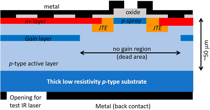
FIGURE 2. Simplified cross-section of an LGAD, not to scale. The p-spray isolation implant between pixels can be replaced by a p-stop implant.
2.1 Substrate
To deliver a fast signal, LGADs must be fabricated on thin silicon substrates, usually in the range of 20–50 μm thick. For example, both experiments ATLAS and CMS plan to use 50 μm thick LGADs as sensors in their timing detectors. However, such thin substrates are impossible to process with equipment normally present in a standard clean-room. The thin active layer, which is depleted under normal operation and where the mips deposit the charge that is responsible for the creation of the signal, may be epitaxially grown over a thick low-resistivity handling wafer. The latter acts both as a mechanical support and as a ohmic contact. Being a sink for the holes, it must be p-type. It is convenient that the thin high-resistivity layer above the p-type low-resistivity bulk is p-type as well. This also prevents the charge-sign inversion after irradiation, commonly observed in n-type substrates, even after modest irradiation levels. Another way to handle such thin wafers is to bond two of them together. One of the wafers would be a thick low-resistivity wafer and the other being a high resistivity wafer which will subsequently be thinned down to the desired thickness by a standard process (e.g. wafer grinding followed by a polishing step, Chemical Mechanical Polishing (CMP) or dry polishing). In both cases, the handling wafer is a low-resistivity and no structures can be fabricated there. It comes that thinned LGADs for fast timing are intrinsically single sided devices: the only pattern that may be present on the back is a patterned metal to allow a laser beam through for testing purposes.
As mips deliver a charge proportional to the thickness of the traversed substrate, a lesser charge is generated in thin active layers and higher gains need to be engineered to achieve the same output charge.
2.2 n+
An LGAD pixel or strip element is defined by an uniform, highly doped shallow n+ region, usually obtained by means of a high-dose phosphorus implantation. This implant is then in contact, at least in part, with an aluminum metalization for the purpose of connecting to the external world by means of wire-bonding or bump-bonding (in which case an under-bump metalization (UBM) is required over the aluminum bump pad). Some n+ regions may be covered by an oxide layer so that the metal contacts the n+ in limited regions only. However, it is important that the resistance path that the signal sees, from the point in which the mip hits within the n+ region and the metal, is negligible. From here the importance of having both a high-doped n+ layer which offers a low resistance to the signal as well as closely spaced contacts. In fact, if LGADs are used for fast-timing applications, they are read-out with wide-bandwidth front-end electronics, order of 1 GHz. The RC associated with the LGAD must be well below 0.1 ns, which is of the same order as the rise time of the signal. The n+ implant on the depleted substrate must be considered as a network of resistance and capacitances (towards the back) so that a signal that is generated at some point is “frozen” for a time RC in the area surrounding the hit position.
Also, ohmic contacts between n+ and aluminum must present very low resistance, which can be achieved by a high-dose phosphorus implantation properly annealed. In the extreme case, if an LGAD is fabricated with a low-dose phosphorus implant as n+ and designed with distant contacts, one may be able to read-out only lower (and broader) signals as we will see in the following sections dedicated to the AC-LGADs.
2.3 Junction Termination Edge
At the border of the n+ and ohmically connected to it, usually a Junction Termination Edge (JTE) is implanted [21]. This is a deep, low dose, phosphorus implant which serves the purpose of reducing the electric fields at the border and assuring that the maximum-value electric fields develop at the junction of the n+/gain layer. In this way, impact ionization in the device only occurs here. It is practical to do this implantation as the first implantation of the process so that it undergoes all the thermal cycles required. This increases the diffusion of the layer and its high-voltage handling capability. A way to implant the JTE deep, even with a sub-maximal implantation energy, is to exploit the channeling effect in silicon by implanting the phosphorus with zero tilt and rotation in a 100 oriented wafer. To still have a high doping concentration at the interface, multiple implantations can also be foreseen for the JTE, with low energies and high doses followed by higher energies and lower doses.
2.4 Gain Layer
The gain layer is a deep, low-dose boron implant, that undergoes full depletion during operation. Typically, the dose is anywhere between about 1.5 1012–5.1012 cm−2 depending on a number of parameters such as substrate thickness and doping as well as profile of the gain layer and its depth. Since it is a critical parameter of the process, it must be carefully controlled and this is usually achieved by ion-implantation. High-energy implantations are best suited for this application. As a rule of thumb, a deeper gain layer requires less implanted dose than a shallower one, so that also the electric field in between the n+ and the gain layer is lower. Since the ratio of the impact ionization for electrons and holes is a function of the electric field (the higher the ratio the lower the field), deeper gain layers are preferred when lower multiplication noises are sought-after. On the other hand, shallower gain-layers are advantageous when considering radiation hardness, because of their higher doping concentration peak. Since the gain depends on a complicated integral of a function of the electric field, the depth of the gain layer plays a crucial role in the gain of an LGAD. As seen in the example of Figure 3, obtained by means of TCAD simulations of possible LGAD structures, the breakdown voltage strongly depends on both the depth and the dose of the gain layer. A peak position in-between 0.4 and 1 μm are achievable with standard implantation energies (up to 400 keV). Given an implantation energy, i.e. a depth for the gain layer, the implantation dose that results in an optimal breakdown voltage (200–300 V) falls within a very limited range of values, so that every care must be taken to develop a consistent and reproducible process flow.
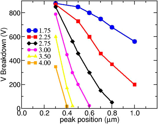
FIGURE 3. Simulated breakdown voltage as a function of the peak position of the gain layer, for different implantation doses of the p-type gain layer (in units of 1012 cm−2). The simulation considers an example of 1-dimensional 50 μm thick LGAD structure and it is for exemplification only.
The gain layer must be contained within the border defined by JTE, otherwise high electric fields develop where the JTE ends due to its curvature. The tip of the gain layer can also be embedded into the JTE, which is usually more doped than the gain layer, provided the JTE is deep enough.
Usually, one wants to numerically simulate the process in order to limit the process splittings during prototyping. Standard impact ionization models in a TCAD simulator may not well reflect the process used and an ad-hoc definition of the parameters must be conducted. At least for the first productions, foundries prefer to process in parallel a few wafers that differ for just one parameter (e.g. dose of the gain layer, by keeping the implantation energy to a maximum) and tune the parameters of their simulations to fit the results.
2.5 p-spray
The gap between pixels is covered by an oxide layer. It is well known that fixed positive oxide charges naturally present at the interface and into the oxide itself induce an electron layer at the oxide/silicon interface. This layer shorts the n+ pixels unless a boron layer, compensating for the electron accumulation layer, is placed in the gap. This problem is present in all silicon sensors and it is solved by implanting either a patterned layer around each pixel (p-stop) or a uniform layer (p-spray) all over the surface, usually at the beginning of the process. The p-stop is generally more doped, by about one order of magnitude, than the p-spray [22]. In LGADs the situation is slightly different, because the p-spray implanted in the active areas (i.e. above the gain layer) would interfere with the gain layer, being both p-type. One approach is to pattern also the p-spray in a fashion very similar to the p-stop case, and implant it just from JTE to JTE of adjacent pixels, while keeping its standard implantation dose, as shown in Figure 2. Being a very low dose implant (order of 2 1012 cm–2), the p-spray can touch or be even embedded in the JTE, without the risk of breakdown. On the other hand, being that the p-stop is more doped, there must be a distance between the JTE and the p-stop to avoid breakdowns. The distance increases the dead-areas of the LGADs, as discussed in the following sections.
3 Electrical Characterization of Low-Gain Avalanche Diodes
After the completion of an LGAD fabrication batch in clean room, a static electrical characterization at the probe station follows. It is useful to place diodes and LGADs close-by on the same wafers. The devices should be perfectly identical, save of course for the presence of the gain layer in the LGAD. A current-voltage curve as the one reported in Figure 4A clearly shows the difference between the two devices. In the diode case, the I-V measures the leakage current dominated by the thermally-generated carriers in the deplete silicon bulk (surface currents are negligible), while for an LGAD this current is amplified by the gain layer. At high voltages, the electric fields between n+ and gain layer are high enough to trigger the impact ionization for the holes, resulting in an avalanche breakdown (in the case reported in Figure 4A this happens at 300 V). Notice that at low voltages, below a few tens of volts, the gain layer is not depleted and the LGAD current is very small. At depletion of the gain layer, the LGAD current jumps up, giving a good estimate of the voltage at which the gain layer depletes. A better evaluation of it can be achieved by performing a capacitance-vs-voltage measurement, as the one shown in Figure 4B. While the gain layer is not yet depleted, the capacitance is very high; at the bias voltage at which it depletes a sharp drop in the capacitance happens (about 18 V in the figure): this feature in the curve C-V is commonly referred to as “foot”. Plotting the capacitance as C−2-V, it is even more apparent where the foot voltage is: it is the voltage at which the curve starts rising linearly from zero. Note that the C-V of the LGAD is translated from the C-V of a diode simply by the foot voltage. From the C-V one can also extract the doping profile of both the gain layer and the substrate. In the devices considered in the figure, the doping concentration of the substrate is uncommonly high (about 7.1013 cm−3, translating in a depletion voltage of 140 V); usually the doping concentration of the substrate is much less, order of 1012 cm−3, as in any High-Resistivity (HR) substrate.
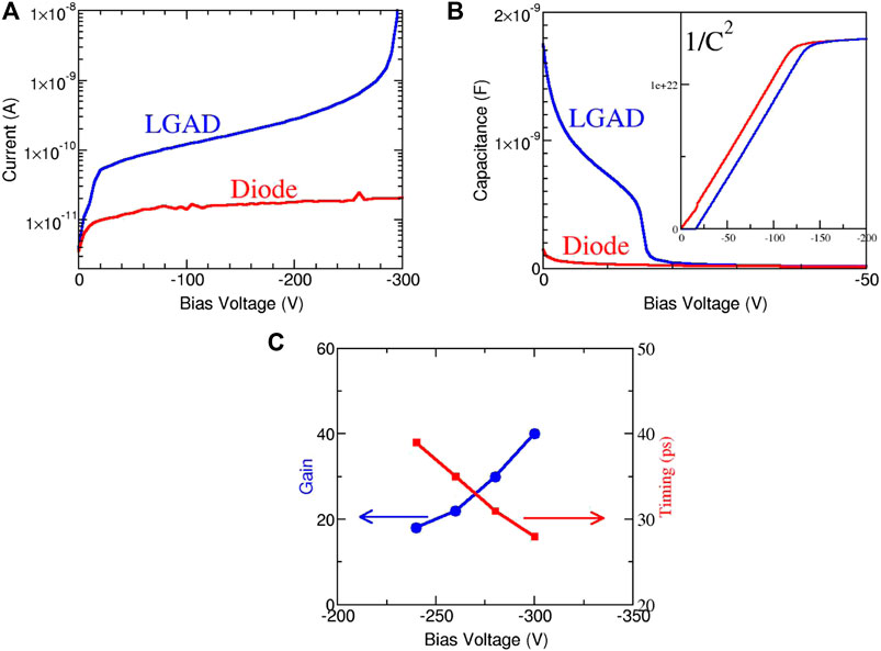
FIGURE 4. Typical plots obtained during the characterization of an LGAD (from a BNL production): (A) current vs bias voltage and (B) capacitance vs bias voltage of an LGAD and a diode fabricated on the same wafer; the diode differs from the LGAD for the absence of the gain layer, which is present in the LGAD. In the inset of (B), C-V plotted as C−2-V. (C) Gain and timing resolution vs bias voltage for the LGAD of (A) and (B).
Functional characterization of an LGAD includes evaluation of the gain and timing resolution vs bias voltage (Figure 4C). This can be done by connecting the device to a fast transimpedance amplifier read-out circuit and exposing the detector to a beam of mips (in laboratory, these are provided by a 90Sr beta source, for example). From the area of the current pulses, once the gain of the electronics has been calibrated, the gain can be extracted. For the timing, at least another device (a scintillator system or another LGAD) of known timing resolution has to be used. Mips are made crossing through all the devices and coincidences are looked at. The timing can be calculated with an off-line analysis. A gain in the order of a few tens is easily achievable before irradiation, while timing resolution, which strongly depends on the gain, can go a bit lower than 30 ps, for 50 μm thick devices.
Figure 5 shows simulated signals generated by a mip vertically crossing either a diode or an LGAD, in this example having a gain of 10. The two devices are both 50 μm thick and are large enough to be considered, with good approximation, 1-dimensional devices. The simulations have been run using the software Weightfield2 [23]. Diodes exhibit a null rise time because the signal starts developing as soon as the carriers move into the bulk. The same is true for the LGAD whose initial part is generated by the same principle. In LGADs for later times, instead of decreasing with time as in the case of the diode, the signal increases because of the contribution of multiplied holes. It can be easily appreciated how most of the signal comes from the drift of the multiplied holes into the depleted substrate. Still, the full signal develops in about one nanosecond.
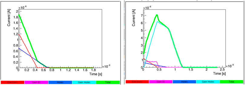
FIGURE 5. Left (Right), Weightfield2 simulations of the signal generated by a mip crossing a 50 μm thick diode (LGADs with gain = 10). V = 200 V. The different contribution to the current of electron, holes, multiplied holes and multiplied electrons are indicated.
All electronics have a limited bandwidth that will introduce a non null rise time, also in the case of the diodes. Moreover, even front-end electronics with a large bandwidth, for example 1 GHz, will spread the relatively long signal of the LGAD signal further. As a consequence the signals of an LGAD or a diode will not be dramatically different, except of course for their amplitude. It must be noted that when reading at high speed, the noise varies as √B, B being the bandwidth and is large for a fast electronics. As a consequence, signals from diodes are beyond detection and only the gain provided by an LGAD makes the signal detectable.
An important parameter to have a fast signal is the electric field that is present into the substrate. While well below the threshold for impact ionization, it still needs to be high enough for the full signal to develop in a short time. For example, if multiplied holes have to drift 50 μm in less than one nanosecond, their drift velocity must be v > μhE = 5.106cm/s, and given the mobility of the holes μh, the electric field must be E > 3.104V/cm. Considering the electric field constant, a voltage of 150 V must fall into the substrate. For operation at low temperatures, where the mobility and therefore the velocity are higher, this requirement is relaxed. But still, an operational voltage slightly in excess of 200 V (for 50 µm thick LGADs) is required for best performance. For thinner substrates, the voltage drop into the substrate scales accordingly to the thickness.
The importance of a high-enough electric field into the substrate is stressed by Figure 6, showing the total pulse currents (sum of the electron and hole contributions) in 1-D LGADs and diodes of different substrate thicknesses, and all biased at the same voltage of 200 V. An identical bias voltage makes the electric field higher, carriers faster and signal shorter (and therefore larger) in thinner devices. Differing from the case of diodes, in which in first approximation the amplitude is the same independently of substrate thickness, signal amplitudes in LGADs tend to decrease with thickness. On the other hand, if the same electric field was present into LGADs of different thicknesses, the current pulses would have the same amplitude [24]. In fact, the lower weighting potential in thick devices is exactly compensated by the larger charge deposited by the mip. The broader pulses in thicker devices are due to the longer time electrons and holes need to drift into the substrate and their integral accounts for the larger deposited charge. From Figure 6 it can also be appreciated how, in LGADs, thicker substrates give origin to slower pulses which lead to worse timing resolutions.
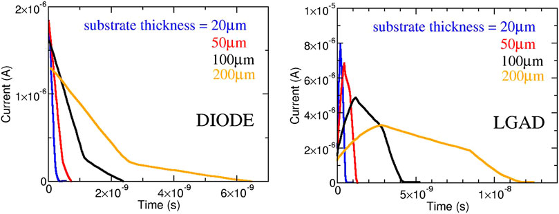
FIGURE 6. Left (Right), Weightfield2 simulations of the signal generated by a mip crossing diodes (LGADs with gain = 10) for different substrate thicknesses, as read-out by an infinite bandwidth electronics. V = 200 V.
5 Timing in Low-Gain Avalanche Diodes
As LGADs have been developed to address timing in mip detection, it is important to state the contributions to the total timing resolution (σt) and how this can drive choices in the layout and fabrication. The timing resolution of LGADs is defined by the following formula:
To minimize the first two terms we can work on the LGAD properties, while the last two require efforts on the read-out electronics (front and back-end).
The first term is the jitter and accounts for the noise (σn) of the detector (LGAD + read-out electronics). It can be minimized with a good design of the front-end and by minimizing the input capacitance. The slew rate (dS/dt) can be increased using large signals (i.e. large gains) and thin substrates biased at voltages high-enough to achieve carrier velocity saturation, as the signals shown in Figure 6 suggest.
The Landau noise (σLandau) is due to the not-uniform generation of charge along the track of the mip, which generates a certain number of electron/hole pairs per micron of silicon that fluctuates around an average amount of 80. Thin substrates exhibit a lower Landau noise. With good electronics in a system where power consumption is not an issues, this is the dominant term. 3D sensors featuring electrodes perpendicular to the surface and therefore parallel to the mip direction, do not suffer from such noise source [25], although only in the particular case of particles crossing parallel to the columns. In this case, they can therefore be intrinsically faster than LGAD, at the price of an increase capacitance.
The time-walk noise is due to the statistical distribution of the signal amplitudes that are derived from the Landau distribution of the charge generated by the mips and the fluctuations in the gain. If the trigger is set at a certain threshold, then signals are detected after different times with respect to the time of arrival. While fast signals are less prone to this error, we can get rid of this effect by applying the Constant Fraction Discrimination method, in which normalized waveforms are triggered.
The last term takes into account the finite binning capabilities of the ADC. Usually this term can be made negligible.
Timing measurements performed with low-noise front-end electronics and sophisticated post processing, which therefore make the terms σ2timewalk+σ2ADC negligible, show how σt is a strong function of the gain and reaches, for gains generally larger than 20, an asymptotic values due to the term σLandau. For 50 micron thick LGADs, as shown in Figure 4, this values can go lower than 30 ps, while for 20 micron thick devices it goes down to 15 ps.
6 Low-Gain Avalanche Diodes for ATLAS and CMS
Both CMS and ATLAS experiments are upgrading their detectors adding a timing sub-detector to help resolve the tracks originating from the many vertexes expected in one bunch crossing: they are the MIP Timing Detector for CMS [26], placed in its Endcap Timing Layer (ETL), and the ATLAS High Granularity Timing Detector (HGTD) [27]. They are required to give a 30 ps timing resolution per track over the full lifetime. This task, which is hard to be accomplished by a single layer, can instead be achieved by having n sensitive layers, therefore having the timing resolution scaling as √n. This translates to a requirement of 52 or 60 ps/hit in the case of three or four independent timing measurements along the particle path [28]. This resolution is achievable with an LGAD of 50 μm active thickness or lower and until a fluence of about 3.1015neq/cm2 is reached. After that the timing resolution of the LGAD has been measured to degrade to a value less than 60 ps, at which time a replacement detector is needed. The sensor pad size is driven by occupancy, pad capacitance, and the fill factor (FF). A unified pad size of 1.3 by 1.3 mm2 in all detectors with an expected capacitance of 3.4 pF is found to fulfill the requirements. The pads will be arranged in arrays that take up a total area of about 20 by 40 mm2 (15 × 30 pixels for ATLAS and 16 × 32 pixels for CMS) with a common backplane bias voltage connection.
CNM was the foundry that first started the fabrication of prototype thin LGADs in 2016, within an RD50 Common Project, for the ATLAS HGTD. They were fabricated on 4” wafers with 50 μm thick active area. The initial substrate was a silicon-on-insulator (SOI) type, with the back-side contact done through the inactive silicon wafer by means of deep wet-etch trench going through the insulator, however they later used Si-on-Si wafers. Splittings of the implantation dose for the multiplication layer were done, ranging from 1.8–2.0 1013 cm−2. Such a high doping concentration was due to the long diffusion time at high temperature used by CNM to anneal the gain layer.
For both experiments, Hamamatsu Photonics (HPK) is delivering LGAD sensors manufactured on Si-Si bonded 6” wafers of 150 μm total thickness with a 35, 50 or 80 μm thick high resistivity float zone (FZ) active layer. Samples with different gain layer doses were produced, sharing the layout, to study the optimum parameters of the charge multiplication mechanism. Eventually a convergence toward 50 μm thickness has been reached. In the wafer layout, for test purposes, circular or square single channel devices have been inserted. Also small arrays are present, differing for the no-gain gap between the pixels.
FBK [29] has produced structures with different interpad distances and widths of the isolation p-stop implants, which are aimed at maximizing the fill factor while keeping good isolation between pads. Besides doing several splittings of the gain layer dose to optimize the performance, they engineered the gain layer as to make it more radiation resistant. In some splittings, the boron of the gain layer has been replaced by gallium, in others a carbon implantation has been added to the gallium or boron implant. If on one hand doping with gallium resulted in a worsening of the overall performance, the carbon co-implantation seems to result in an increased radiation resistance while keeping the same timing performance, at the expense of an increased leakage current.
Recently, also IHEP-NDL has joined the effort of prototyping of LGADs structures (single pixels and arrays) for the ATLAS HGTD [30].
7 Limitations of Low-Gain Avalanche Diodes
With the help of Figure 7 let’s consider what happens at the border of an LGAD pixel. The figure reports the electrostatic potential map of a 2-D LGAD, 50 μm thick. To simulate the interpixel capacitance and the charge sharing between two adjacent pixels, a pixel on the right of the one shown in figure has been included in the simulation. Being the two pixels identical, the boundary line at X = 75 μm is an axis of symmetry for the device. Far away from the JTE and well within the gain layer, electric field lines are vertical and parallel to each other. Electrons generated here drift to the n+ and get multiplied as expected. If mips pass outside the gain layer (for X larger than 60 μm in this example), the generated electrons are collected by the JTE and are not amplified. For mips passing through this region, an LGAD behaves as a diode (gain = 1) and the signals will most likely be under the threshold for detection with fast electronics. There is an intermediate region where the electric field lines point to the JTE, so that electrons are partially collected here and do not go through the gain layer: the signal is subjected to a partial amplification. In Figure 8 the current pulses and their integrals (i.e. total collected charge) generated by mips crossing at different X is plotted. In the LGAD, the signal generated by a mip crossing outside the gain layer is not different from the signal generated by a mip crossing at the center of a diode. Mips crossing close to the end of the gain layer (the gain layer in this example ends at X = 60 μm) give origin to a smaller signal, but still no net charge is collected by the nearby pixel. At X = 75 μm, which is mid gap, the same signal is induced in both pixels and the charge is shared between the two. This example makes apparent that a dead region at the border of an LGAD pixel exists, which can easily be larger than 20 μm. Fine pitch strip and pixels, with pitches in the order of 100 μm, are therefore excluded in the LGAD basic technology as the dead areas will be intolerably large. For example, LGADs to be used by either CMS or ATLAS have a pitch, as said above, of 1.3 mm.
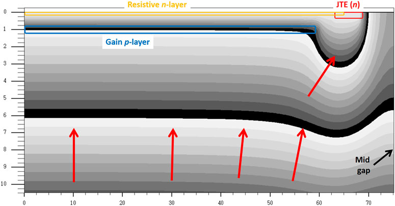
FIGURE 7. Map of the electrostatic potential in the example of LGAD simulated. Only the part of the structure to the left of the mid gap is shown. Red Arrows show the trajectories of electrons.
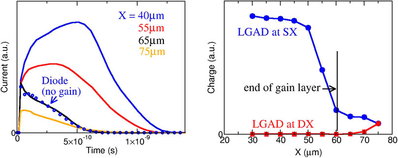
FIGURE 8. Left, simulated current pulses at the left electrode (SX) of Figure 7 generated by mips crossing the device vertically at position X as specified in the legend. Solid lines are for an LGAD with gain of 10, the dotted line is for the case of a mip crossing the diode at X = 40. Right, charge calculated as the integral of the current pulses produced by mips traversing the silicon at X, and induced at the electrode on the left (SX) and on the right (DX).
To minimize the problem and still use the standard technology to fabricate an LGAD, one can use some design or system features. One can design the JTE as narrow as possible, or design the gain layer tip close to the JTE, or even use p-spray instead of p-stop to have the pixels closer. A high voltage tends to straighten the electric field lines and, therefore, increase the active area. Bringing the pixel closer usually means an increase to the interpixel capacitance which, due to the fast read-out, will add to the noise. In the next subsection we will see how this increase is negligible for an LGAD.
7.1 Capacitance of an Low-Gain Avalanche Diode
For a 1 × 1 mm LGAD fabricated on a 50 μm substrate, its capacitance toward the back is 2 pF. The simulations reported in Figure 9 show that, also in the case of a gap of 20 μm, the interpixel capacitance for a 4 mm perimeter is about 0.2 pF, which is much less than the contribution of the capacitance toward the back. It is interesting to see how the interpixel capacitance is strongly dependent on the substrate thickness. This happens because the substrate acts as an electrostatic shield from one pixel to the other and the shield is as more effective as it is closer to the pixels. The simulations consider the gap as depleted, which is usually not the case, being p-spray or p-stop is present. These resistive layers cause a long-range capacitive coupling between far-away pixels, which increases the interpixel capacitance. However, this contribution is frequency dependent and expected to be unimportant at high frequencies.
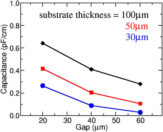
FIGURE 9. TCAD simulations of the interpixel capacitance as a function of the gap between pixels, for different substrate thicknesses.
7.2 Radiation Hardening of Low-Gain Avalanche Diodes
To some extent, LGADs need to be radiation hard to be used in HEP experiments. Several irradiation campaigns clearly pointed out how the gain decreases with hadron fluence (proton irradiation being more damaging than neutron irradiation) [31]. The gain almost vanished at irradiation fluences of about 1015 cm−2. The effect is attributed to the effective acceptor removal in the gain layer [32]. By means of SIMS measurements [33] it has been shown that the boron ion is in the same position as before irradiation, and most likely inactivated by becoming interstitial and forming defect complexes with oxygen. To counteract this effect, two strategies have been tried: 1) replace the boron implant with gallium implant, and 2) implant a carbon spray over the gallium or the boron. The first option is motivated by the fact that the gallium atom may hardly form complexes, being less mobile than silicon. The second option is motivated by the fact that carbon can intercept interstitial silicon, and form Si-C complexes, which have been observed in irradiated silicon. It is measured [33] that a carbonated gain layer is at least a factor of two more radiation resistant than the equivalent non-carbonated gain layer, while gallium doping is less radiation resistant than boron doping.
Furthermore, narrower gain layer implants are more radiation resistant than wider implants due to the higher boron peak concentration of the former, suggesting to keep the annealing of the gain layer as the last thermal step of the process flow while keeping the temperature to a minimum (about 700–800°C).
Another important aspect of radiation hardness of LGADs is their leakage current. In unirradiated devices, the bulk thermally generated leakage current is approximately multiplied by the gain factor. During exposure to irradiation, the gain decreases, so the increase in leakage current is mitigated by the decrease of multiplication. A thin substrate will eventually have a leakage current close to the leakage of a standard, thicker device without amplification.
Furthermore, thinner LGADs (less than 50 μm) are more radiation resistant than thicker ones: while the gain layer contributes less to the electric field because of the acceptor removal process, acceptors are created in the bulk by the radiation. By increasing the bias, in parts of the substrate the electric field can reach the threshold for impact ionization and compensate for the gain layer.
8 Towards 4D Sensors
As discussed in previous sections, pixel dimensions must be by far larger than the substrate thickness to have a uniform multiplication and to maximize the fill-factor. With the current LGAD designs, position resolution in the order of 10 μm, as needed in 4D detectors, is out of reach. Other structures, still based on LGADs, can be developed to have both high spatial and timing resolution. In order to obtain a uniform amplification throughout the whole sensor area, together with high spatial resolution, it is possible to move the n+ and gain layer on one side of the wafer (i.e. the top of the wafer) and the hole collecting electrodes to the opposite side (i.e. the bottom of the wafer) [13, 34]. The hole-collecting electrodes can be placed at a small pitch, without compromising the uniform multiplication occurring at the opposite side of the wafer. To safely process double-sided wafers it requires a wafer thickness of about 200 μm for 4” wafers, and thicker for 6” wafers. Such thicknesses will spoil the timing capability of the LGAD. As an example, the structure can be used for soft X-ray detection where timing information is not crucial.
Another solution to increase the fill factor, but without reaching 100%, is to separate the pixels by small trenches. In this case, pixels can be very close, order of 5 μm, since trenches can be narrower than 1 μm. A trench depth of a few microns is enough for this purpose and it is easily achieved since trenches with aspect ration of 20:1 are fairly common. Moreover, the JTE can be removed since trenches prevent the formation of high electric fields at the edge of the n+. This solution has been implemented by FBK [35], reaching a dead area of only 7 μm between pixels, and has been addressed as “Trench-Isolated LGAD” (TI-LGAD). In their technology, segmented LGADs with pixel pitch down to 50 μm feature a fill-factor higher than 75%. The same parameters for the ion implantation dose and energy of the doped regions, as well as the thermal budget, used in standard LGAD productions are applied to fabricate the TI-LGADs. No detrimental effects due to the introduction of the trench have been experimentally observed.
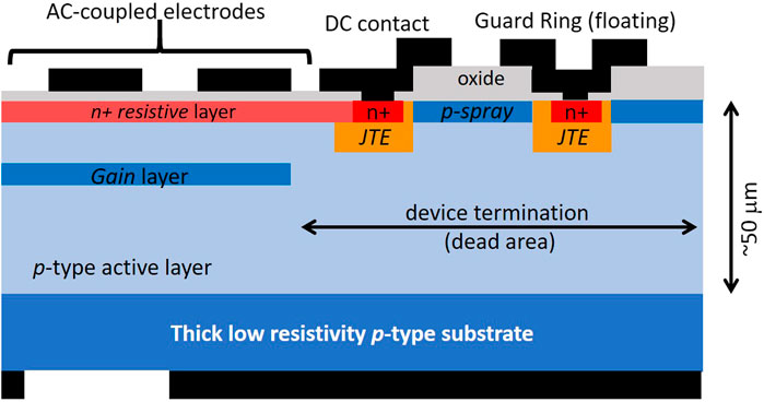
A third solution will be discussed extensively in the following section: it is the AC-coupled LGADs (AC-LGADs for short), also called Resistive Silicon Detectors (RSDs), and is sketched in Figure 10 [36, 37].
9 Structure of an AC-Low-Gain Avalanche Diode
The AC-LGAD consists of a uniform gain layer that, as in the standard LGAD, is implanted deep below the n-implant: these two layers run seamlessly overall the active area [38]. The JTE is implanted at the border and within it a high-dose n+-implant can be present, which is grounded during operation to drain the leakage current as well as the multiplied signal electrons. A main difference is that, in the AC-LGAD, the large uniform n-implant is about 10 or 100 times less doped than the n+ implant of a standard LGAD. Its sheet resistivity is therefore much larger. The gain layer is implanted in the usual way as in the case of the LGAD, its tip can be either embedded in the JTE or stopped at a certain distance from it. Because of the relatively low implantation dose of the n implant, a non-negligible part of the n implant is depleted by applying the operation voltage. This results in the gain layer being effectively deeper (since the depth is measured from the undepleted n implant). As such, the ionization integral is higher for the same doping of the gain layer (i.e. same electric field) which lowers the value of the breakdown voltage compared to that of an LGAD which uses the same gain implant parameters. Therefore, it is necessary to re-calibrate the dose of the gain layer by lowering as much as needed to have a desired breakdown voltage. Notice that this calibration must be conducted for each new dose of the n-implant, although TCAD simulations can help in the selection of the correct dose once they are correctly tuned on the particular process used and reliable.
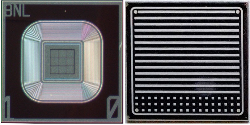
The n-implant is covered by a thin dielectric layer which is typically silicon oxide, silicon nitride, or both, while remaining grounded through a contact at its border. Over the dielectric, there are finely patterned metal electrodes (of arbitrary shape) visible in Figure 11, which will be connected to the read-out electronics. Signals are generated in the usual way and they induce a current pulse to the metal electrodes through the capacitance, whose parallel plates are defined by the metal electrodes and the n+. A 100% fill factor is achieved, with uniform multiplication and no dead areas. Since the metal electrodes are separated from the n-layer by an insulator, they do not collect charge and the signal pulse is bipolar. Since two neighbor electrodes see, through the capacitance, a small resistance between them (due to the n layer), the pixels experience an important cross-talk. On one hand, this increases the position resolution by interpolation. On the other, it increases the occupancy. These effects must be carefully considered when designing the system, especially when a high count rate is expected.
There are a few components which are common in LGADs and AC-LGADs, i.e. the substrate, the JTE and the p-spray. The JTE is still placed at the border of the n-implant that defines the active area, while the p-spray is external to the active area and serves to insulate the JTE from the guard ring termination.
10 Pulse Shape in AC-Low-Gain Avalanche Diodes
In an AC-LGAD, the signal develops in a very similar fashion as in a standard DC-coupled LGAD, with mip-generated electrons crossing the high-electric field and undergoing impact ionization. Multiplied holes then drift towards the substrate, generating most of the signal. In AC-LGADs, however, once electrons arrive at the n-implant they are not immediately collected by the read-out electronics. Instead they continue to generate signal as they move within the n-implant towards the n+ electrode at the border. The resistive n-implant can be seen as a distributed RC network, made by capacitances towards the back and toward the AC-coupled metal electrodes. These capacitances are connected by resistances which account for the finite resistivity of the n-implant. Capacitances and resistances can, up to a certain extent, be tuned by means of the technology process flow. A large capacitance, for the same area of the AC-coupled electrodes, can be obtained using a thin insulator whose ultimate thickness is limited by the critical electric field that the insulator can stand. A large resistance, beside separating by design the metal electrodes, can be obtained by using a low-dose implantation for the n-layer. To avoid a full depletion of the n-layer, its dose must be larger than the integral of the acceptor concentration in the bulk, which include the p-type gain layer and the p-type substrate. The latter contribution is usually negligible. A minimum implantation dose for the n-implantation of about 1.1013cm−2 is therefore needed.
For illustration purposes, a simplified 2-dimensional AC-LGAD structure has been numerically simulated, featuring five AC-coupled electrodes at a pitch of 100 μm and a grounded contact at the edge of the device. The value of the gap between two neighbour AC-coupled metals and the implantation dose of the n-layer have been varied. A mip vertically crosses the silicon in the middle of the device, at the center of the electrode labeled “hit strip” in Figure 12 and in Figure 13, where some results are presented. It has been verified that the signal at the substrate is independent on the explored range of parameters (once the AC-LGADs are operated at the same gain) and closely matches the signal induced in a standard LGAD.
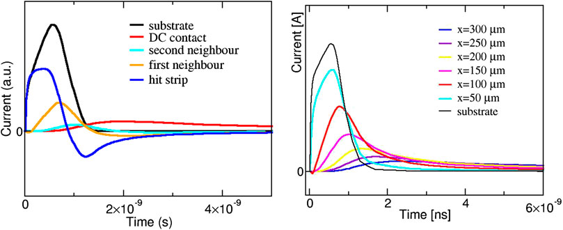
FIGURE 12. Left, current pulses at different electrodes as an example of simulated AC-LGAD. Right, for the same example, current pulses at the DC contact for different interaction points X of the mip.
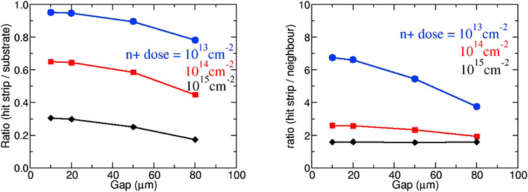
FIGURE 13. Left, ratio of current pulse amplitudes at the substrate and at the hit electrode as a function of the gap between electrodes, for different n+ implantation doses, in the simulated example of AC-LGAD. Right, for the same example, ratio of amplitudes for hit strip and neighbor strip.
In the simulated configuration that considers only the particular case of a mip crossing at the center of an AC-pad, the signal sees a capacitance “C” toward the metal electrode of the “hit strip” [Z = (ωC)−1] and a resistance “R” towards the neighbour electrodes. The current signal splits according to the ratio of the two impedances, as in a conventional current divider. For example, the fast drift of the multiplied holes is fed through “C” unless “R” is very low. Electrons, once arrived at the n-implant, freeze on a limited area because of the non-null resistance of the n-implant and then decay with time constant RC. The motion of the electrons toward the n+ contact, with the time constant RC, accounts for a negative lobe in the current pulse. It is found that the ratio Vhit−Strip/VSubstrate, with Vhit−Strip being the pulse amplitudes at the hit strip and similarly VSubstrate the pulse amplitude at the substrate, depends on the n-implant doping concentration, and decreases as the dose is increased. In fact, by increasing the dose, the effective interpixel resistance R decreases as it becomes comparable to (ωC)−1. A larger share of current is therefore induced at the nearby metals. An increase of the cross-talk is also calculated, which come at the price of lower signals at all electrodes. The effect of the gap is also visible. By reducing the gap, “R” decrease but at the same time “C” does not: the two effects compensate and a weak dependence on the gap is calculated showing that a pitch-to-gap ratio of 1:1 should be adequate in most applications. Further work is in progress aiming to optimize the geometry of the AC-pads. The signal formation in AC-LGAD itself is still debated and more rigorous study is needed to address the topic.
10.1 Considerations on Timing on AC-Low-Gain Avalanche Diodes
The current signal at the substrate is unipolar and essentially identical to the signal delivered by an LGAD, since electrons slowly moving within the n layer are far away from the substrate and marginally contribute to its signal. Since current signals are induced in multiple AC-coupled electrodes, for the same gain the signals at these electrodes necessarily have lower amplitude than in LGADs. Being the signals smaller, the jitter noise term in an AC-LGAD is therefore larger. Moreover, signals at neighbor strips, besides featuring smaller amplitudes, have longer rise times because of resistive effects. This produces even smaller slew rates and makes the jitter term much higher for these strips. On the other hand, profiting from the unavoidable presence of cross-talk, one can take the signals from two or more electrodes and average their time stamp. The timing resolution, in the case of equal noise contribution from the n different strips, scales as √(n). However, for the sensor tested in [39], no significant improvement to the time resolution has been observed when combining measurements from multiple strips in the same cluster [39] which indicates that the former effects dominate.
10.2 Signal at the DC Contact
The DC contact to the n+, which may be embedded into the JTE at the border of the active area, serves as drain for the leakage current and for the signal electrons. Figure 12 shows interesting properties of the signal at the DC contact. Due to the RC network introduced by the n implant, the amplitude of the signals at the DC pad decreases as its distance from the hit coordinate increases. Being the total collected charge is the same and independent from the distance, the smaller signals are broader. Timing resolution associated with this electrode is therefore very poor. On the other hand, mips that hit the active area very close to the DC contact originate pulses very similar to a DC-LGAD, and can therefore be used for gain estimation.
11 Discussion
Leveraged by the interest of the HEP community in its fast timing performance, LGADs have reached an advanced stage of maturity. The physics reach of two mayor experiments in HEP (ATLAS and CMS) critically depends on the performance of meter-squared detectors based on this technology. A few foundries around the world are active in the development of the device, pursuing slightly different approaches in the fabrication but all converging toward the basic structure discussed above. During the years of research, several parameters have been explored, such as substrate thickness and doping of the gain layer, allowing an optimization and a deep understanding of the response of the device. Performance of LGADs coming from different vendors are very similar, although some process parameters such as the profile of the gain layer (mainly, the depth and, consequently, the dose) differ from one vendor to the other. Some other parameters are different as well, for example the depth of the JTE preventing early breakdown at the edges or the use of a p-stop rather than the p-spray, but the basic structure of an LGAD is essentially the same. A point of weakness of the device is its radiation tolerance, limited by the acceptor removal phenomenon which de-activates the boron of the gain layer, lowering the gain below the minimum value necessary to achieve a useful timing resolution. This limitation is particular severe in HEP experiments, where irradiation levels that destroy the gain are easily met. Some efforts are under way to extend the lifetime of the device by engineering the gain layer (carbon spray and low diffusion boron implant), and it is expected that a consistent effort in the LGAD R&D will focus on this topic in the near future.
Other lines of research equally originate from another fundamental limitation of the LGADs: their poor spatial resolution. In fact, LGADs are fabricated as large pixels (order of about 1 mm, much larger than the substrate thickness), thus preventing the possibility of having a device with very good spatial and timing resolution (a 4-D device). A device which has been conceived to solve this issue is the AC-LGAD (also called RSD). Its optimization is complicated by the fact that, besides the gain layer, also the n-layer plays a paramount role in its behaviour and the two implants are intertwined. An intense testing activity is necessary, and is under way, to characterize its performance. While radiation hardness of such devices has not been tested yet, it is expected to be at the same level as in the standard LGADs. 4-D detection is critical in other fields, such as X-ray detection or medical applications, and it may be that the development of such device (or other LGAD-based devices with different structures but similar capabilities) will be pushed from the outside of the HEP community.
Author Contributions
The author confirms being the sole contributor of this work and has approved it for publication.
Funding
This material is based upon work supported by the U.S. Department of Energy under grant DE-SC0012704. This research used resources of the Center for Functional Nanomaterials, which is a U.S. DOE Office of Science Facility, at Brookhaven National Laboratory under Contract No. DE-SC0012704.
Conflict of Interest
The author declares that the research was conducted in the absence of any commercial or financial relationships that could be construed as a potential conflict of interest.
Acknowledgments
The author wishes to thank his colleagues at Brookhaven National Laboratory: Ronald Angona, Wei Chen, Gabriele D’Amen, Sean Robinson, Enrico Rossi, Alessandro Tricoli.
References
1. Hartmann F. Evolution of silicon sensor technology in particle physics. New York, NY: Springer (2009).
2. Aad G, Abat E, Abdallah J, Abdelalim AA, Abdesselam A, Abdinov O, et al. The ATLAS experiment at the CERN large hadron collider. J Inst (2008) 3:S08003. doi:10.1088/1748-0221/3/08/S08003
3. Chatrchyan S, Hmayakyan G, Khachatryan V, Sirunyan AM, Adam W, Bauer T, et al. The CMS Experiment at the CERN LHC. J Inst (2008) 3:S08004. doi:10.1088/1748-0221/3/08/S08004
4. Cartiglia N, Arcidiacono R, Baldassarri B, Boscardin M, Cenna F, Dellacasa G, et al. Tracking in 4 dimensions. Nucl Instr Methods Phys Res Section A: Acc Spectrometers, Detectors Associated Equipment (2017) 845:47–51. doi:10.1016/j.nima.2016.05.078
5. Sadrozinski HFW, Ely S, Fadeyev V, Galloway Z, Ngo J, Parker C, et al. Ultra-fast silicon detectors. Nucl Instr Methods Phys Res Section A: Acc Spectrometers, Detectors Associated Equipment (2013) 730:226–31. doi:10.1016/j.nima.2013.06.033
6. Cartiglia N, Arcidiacono R, Borghi G, Boscardin M, Costa M, Galloway Z, et al. LGAD designs for future particle trackers. Nucl Instr Methods Phys Res Section A: Acc Spectrometers, Detectors Associated Equipment (2020) 979:164383. doi:10.1016/j.nima.2020.164383
7. Pellegrini G, Fernández-Martínez P, Baselga M, Fleta C, Flores D, Greco V, et al. Technology developments and first measurements of Low Gain Avalanche Detectors (LGAD) for high energy physics applications. Nucl Instr Methods Phys Res Section A: Acc Spectrometers, Detectors Associated Equipment (2014) 765:12–6. doi:10.1016/j.nima.2014.06.008
8. Giacomini G, Chen W, Lanni F, Tricoli A. Development of a technology for the fabrication of low-gain avalanche diodes at BNL. Nucl Instr Methods Phys Res Section A: Acc Spectrometers, Detectors Associated Equipment (2019) 934:52–7. doi:10.1016/j.nima.2019.04.073
9. Paternoster G, Arcidiacono R, Boscardin M, Cartiglia N, Cenna F, Betta GD, et al. Developments and first measurements of ultra-fast silicon detectors produced at FBK. J Inst (2017) 12(02):C02077. doi:10.1088/1748-0221/12/02/c02077
10. Yang X, Alderweireldt S, Atanov N, Ayoub M, da Costa JBG, Garca LC, et al. Layout and performance of HPK prototype LGAD sensors for the high-granularity timing detector. Nucl Instr Methods Phys Res Section A: Acc Spectrometers, Detectors Associated Equipment (2020) 980:164379. doi:10.1016/j.nima.2020.164379
11. Fan Y, Alderweireldt S, Agapopoulou C, Atanov N, Ayoub MK, Caforio D, et al. Radiation hardness of the low gain avalanche diodes developed by NDL and IHEP in China. Nucl Instr Methods Phys Res Section A: Acc Spectrometers, Detectors Associated Equipment (2020) 984:164608. doi:10.1016/j.nima.2020.164608
12. Moffat N, Bates R, Bullough M, Flores L, Maneuski D, Simon L, et al. Low Gain Avalanche Detectors (LGAD) for particle physics and synchrotron applications. J Inst (2018) 13:C03014. doi:10.1088/1748-0221/13/03/c03014
13. Pellegrini G, Baselga M, Carulla M, Fadeyev V, Fernández-Martínez P, García MF, et al. Recent technological developments on LGAD and iLGAD detectors for tracking and timing applications. Nucl Instr Methods Phys Res Section A: Acc Spectrometers, Detectors Associated Equipment (2016) 831:24–8. doi:10.1016/j.nima.2016.05.066
14. Shah KS, Farrell R, Grazioso R, Myers R, Cirignano L. Large-area APDs and monolithic APD arrays. IEEE Trans Nucl Sci (2001) 48(6):2352–6. doi:10.1109/23.983267
15. Tapan I, Gilmore R. Simulation of signal generation for silicon avalanche photodiodes (APDs). Nucl Instr Methods Phys Res Section A: Acc Spectrometers, Detectors Associated Equipment (2000) 454(1):247–51. doi:10.1016/S0168-9002(00)00835-4
16. Centis Vignali M, Dias De Almeida P, Franconi L, Gallinaro M, Gurimskaya Y, Harrop B, et al. Deep diffused Avalanche photodiodes for charged particles timing. Nucl Instr Methods Phys Res Section A: Acc Spectrometers, Detectors Associated Equipment (2020) 958:162405. doi:10.1016/j.nima.2019.162405
17. Karar A, Musienko Y, Vanel JC. Characterization of avalanche photodiodes for calorimetry applications. Nucl Instr Methods Phys Res Section A: Acc Spectrometers, Detectors Associated Equipment (1999) 428(2):413–31. doi:10.1016/s0168-9002(99)00177-1
18. Baron AQR, Kishimoto S, Morse J, Rigal J-M. Silicon avalanche photodiodes for direct detection of X-rays. J Synchrotron Radiat (2006) 13(2):131–42. doi:10.1107/s090904950503431x
19. Shah KS, Farrell R, Grazioso RF, Cirignano L, Squillante MR, Entine G. “Planar processed APDs and APD arrays for scintillation detection”, in IEEE Nuclear Science Symposium. Conference Record. 1999 Nuclear Science Symposium and Medical Imaging Conference (Cat. No.99CH37019), Seattle, WA, October 24–30, 1999 IEEE (1999), 56–60.
20. Ramo S. Currents induced by electron motion. Proc IRE (1939) 27:584–5. doi:10.1109/jrproc.1939.228757
21. Fernndez-Martnez P, Flores D, Hidalgo S, Greco V, Merlos A, Pellegrini G, et al. Design and fabrication of an optimum peripheral region for low gain avalanche detectors. Nucl Instr Methods Phys Res Section A: Acc Spectrometers, Detectors Associated Equipment (2016) 821:93–100. doi:10.1016/j.nima.2016.03.049
22. Piemonte C. Device simulations of isolation techniques for silicon microstrip detectors made on p-type substrates. IEEE Trans Nucl Sci (2006) 53:1694–705. doi:10.1109/tns.2006.872500
23. Cenna F, Cartiglia N, Friedl M, Kolbinger B, Sadrozinski HFW, Seiden A, et al. Weightfield2: a fast simulator for silicon and diamond solid state detector. Nucl Instr Methods Phys Res Section A: Acc Spectrometers, Detectors Associated Equipment (2015) 796:149–53. doi:10.1016/j.nima.2015.04.015
24. Cartiglia N, Arcidiacono R, Bellora A, Cenna F, Cirio R, Durando S, et al. The 4D pixel challenge. J Inst (2016) 11(12):C12016. doi:10.1088/1748-0221/11/12/c12016
25. Kramberger G, Cindro V, Flores D, Hidalgo S, Hiti B, Manna M, et al. Timing performance of small cell 3D silicon detectors. Nucl Instr Methods Phys Res Section A: Acc Spectrometers, Detectors Associated Equipment (2019) 934:26–32. doi:10.1016/j.nima.2019.04.088
26.CMS Collaboration. A MIP timing detector for the CMS phase-2 upgrade (2019). Report No.: CERN-LHCC-2019-003. CMS-TDR-020 Meyrin, Switzerland: CERN. Available at https://cds.cern.ch/record/2667167?ln=en
27.Technical Design Report. A high-granularity timing detector for the ATLAS phase-II upgrade (2020). Report No.: CERN-LHCC-2020-007. ATLAS-TDR-031 Meyrin, Switzerland: CERN. Available at https://cds.cern.ch/record/2719855?ln=en
28. Cartiglia N, Staiano A, Sola V, Arcidiacono R, Cirio R, Cenna F, et al. Beam test results of a 16ps timing system based on ultra-fast silicon detectors. Nucl Instr Methods Phys Res Section A: Acc Spectrometers, Detectors Associated Equipment (2017) 850:83–8. doi:10.1016/j.nima.2017.01.021
29. Sola V, Arcidiacono R, Boscardin M, Cartiglia N, Dalla Betta G-F, Ficorella F, et al. First FBK production of 50μm ultra-fast silicon detectors. Nucl Instr Methods Phys Res Section A: Acc Spectrometers, Detectors Associated Equipent (2019) 924:360–8. doi:10.1016/j.nima.2018.07.060
30. Xiao S, Alderweireldt S, Ali S, Allaire C, Agapopoulou C, Atanov N, et al. Beam test results of IHEP-NDL low gain avalanche detectors (LGAD). (2020)
31. Kramberger G, Baselga M, Cindro V, Fernandez-Martinez P, Flores D, Galloway Z, et al. Radiation effects in low gain avalanche detectors after hadron irradiations. J Inst (2015) 10(7):P07006. doi:10.1088/1748-0221/10/07/p07006
32. Moll M. Acceptor removal-displacement damage effects involving the shallow acceptor doping of p-type silicon devices, The 28th International Workshop on Vertex Detectors, Lopud, Croatia, October 13–18, 2019 (2020), 27. doi:10.22323/1.373.0027
33. Ferrero M, Arcidiacono R, Barozzi M, Boscardin M, Cartiglia N, Betta GD, et al. Radiation resistant LGAD design. Nucl Instr Methods Phys Res Section A: Acc Spectrometers, Detectors Associated Equipment (2019) 919:16–26. doi:10.1016/j.nima.2018.11.121
34. Dalla Betta GF, Pancheri L, Boscardin M, Paternoster G, Piemonte C, Cartiglia N, et al. Design and TCAD simulation of double-sided pixelated low gain avalanche detectors. Nucl Instrum Meth Phys Res A (2015) 796:154–7. doi:10.1016/j.nima.2015.03.039
35. Paternoster G, Borghi G, Boscardin M, Cartiglia N, Ferrero M, Ficorella F, et al. Trench-Isolated low gain avalanche diodes (TI-LGADs). IEEE Electron Device Lett (2020) 41(6):884–7. doi:10.1109/led.2020.2991351
36. Mandurrino M, Arcidiacono R, Boscardin M, Cartiglia N, Dalla Betta GF, Ferrero M, et al. Demonstration of 200-, 100-, and 50- μ m pitch resistive AC-coupled silicon detectors (RSD) with 100 fill-factor for 4D particle tracking. IEEE Electron Device Lett (2019) 40(11):1780–3. doi:10.1109/led.2019.2943242
37. Giacomini G, Chen W, D'Amen G, Tricoli A Fabrication and performance of AC-coupled LGADs. J Inst (2019) 14(9):P09004. doi:10.1088/1748-0221/14/09/p09004
38. Mandurrino M, Arcidiacono R, Boscardin M, Cartiglia N, Dalla Betta GF, Ferrero M, et al. Analysis and numerical design ofrResistive AC-coupled silicon detectors (RSD) for 4D particle tracking. Nucl Instr Methods Phys Res Section A: Acc Spectrometers, Detectors Associated Equipment (2020) 959:163479. doi:10.1016/j.nima.2020.163479
Keywords: silicon detectors, high-energy physics, impact ionization, fabrication process, timing, avalanche photodiodes
Citation: Giacomini G (2021) Fabrication of Silicon Sensors Based on Low-Gain Avalanche Diodes. Front. Phys. 9:618621. doi: 10.3389/fphy.2021.618621
Received: 17 October 2020; Accepted: 14 January 2021;
Published: 05 April 2021.
Edited by:
Angela Kok, Sintef Digital, NorwayReviewed by:
Giovanni Paternoster, Bruno Kessler Foundation (FBK), ItalyMarco Mandurrino, National Institute of Nuclear Physics of Turin, Italy
Copyright © 2021 Giacomini. This is an open-access article distributed under the terms of the Creative Commons Attribution License (CC BY). The use, distribution or reproduction in other forums is permitted, provided the original author(s) and the copyright owner(s) are credited and that the original publication in this journal is cited, in accordance with accepted academic practice. No use, distribution or reproduction is permitted which does not comply with these terms.
*Correspondence: Gabriele Giacomini, Z2lhY29taW5pQGJubC5nb3Y=
 Gabriele Giacomini