
94% of researchers rate our articles as excellent or good
Learn more about the work of our research integrity team to safeguard the quality of each article we publish.
Find out more
ORIGINAL RESEARCH article
Front. Phys. , 14 January 2021
Sec. Radiation Detectors and Imaging
Volume 8 - 2020 | https://doi.org/10.3389/fphy.2020.607319
This article is part of the Research Topic Advanced fabrication technologies for semiconductor radiation detectors View all 13 articles
 Lodovico Ratti1,2*
 Paolo Brogi3,4
 Gianmaria Collazuol5,6
 Gian-Franco Dalla Betta7,8
 Pier Simone Marrocchesi3,4
 Lucio Pancheri7,8
 Arta Sulay3,4
 Gianmarco Torilla1,2
 Carla Vacchi1,2
This paper reports the characterization of SPAD arrays fabricated in a 150 nm CMOS technology in view of applications to the detection of charged particles. The test vehicle contains SPADs with different active area and operated with different quenching techniques, either passive or active. The set of devices under test (DUTs) consists of single-tier chips, about 30 mm2 in area, with dual-tier structures where two chips are face-to-face bump bonded to each other. In the dual-layer structure obtained in this way, the coincidence signal between overlapping SPAD pairs is read out, with a beneficial impact on the dark count noise performance. The DUT characterization was mainly focused on studying the breakdown voltage in the single-layer arrays and the dark count rate (DCR), measured in different working conditions, in both the single- and the dual-layer structures. Comparison between the DCR performance of the two configurations clearly emphasizes the advantage of the coincidence readout architecture.
In applications at the next generation linear colliders and B-factories, the need for accurate vertex measurements will call for highly granular and light detectors (typically less than 0.1% of the radiation length), to be placed very close to the beam interaction regions. In order to comply with these low material budget requirements, during the last 2 decades new detector technologies have been considered. Most of the investigated approaches are based on the integration of the front-end electronics and the sensitive part in the same substrate. This is the case of monolithic active pixel sensors (MAPS), fabricated in different flavors of CMOS technologies [1–4], leveraging their small intrinsic capacitance to achieve fully satisfactory noise performance despite their relatively small active region thickness.
The features of single photon avalanche diodes, or SPADs, mainly used to capture faint optical signals in applications such as optical ranging, fluorescence lifetime imaging, positron emission tomography and Raman spectroscopy [5–8], might also be beneficially exploited for charged particle tracking. As opposed to PIN diodes, providing a signal proportional to the incident radiant power, SPADs can take advantage of a huge internal gain, with no need for pre-amplification (therefore reducing power dissipation), and high spatial and time resolution. Moreover, the amount of detector material can be kept to a minimum, as the sensitive volume of a SPAD is limited to the very thin depleted region around the pn junction. Use of a CMOS technology for the fabrication of the sensor lends itself naturally to monolithically integrating the processing electronics and the sensing element in a common substrate. On the other hand, noise performance of SPADs, usually represented through the dark count rate (DCR) parameter, can jeopardize their capabilities as charged particle detectors. Vertical integration of two SPAD layers has been proposed as a DCR mitigation strategy [9]. More recently, in the frame of the APiX2/ASAP collaboration, funded by the Italian Institute for Nuclear Physics (INFN), the first prototype of a two-tier SPAD detector, providing a coincidence signal when a particle simultaneously strikes two overlapping sensors and significantly reducing the DCR, was successfully tested [10]. While radiation resistance in SPADs is in general poor, with non negligible increase in DCR already at 1 MeV neutron equivalent fluences in the order of 109 cm−2 in devices with a 200 μm3 active volume [11], the coincidence signal approach is expected to mitigate the effect of the radiation susceptibility of the individual layer on the radiation tolerance performance of the bi-layered system.
This paper presents the characterization of SPAD arrays, targeting charged particle tracking in low rate, relatively clean environments, such as the experiments at the future linear colliders [12]. The DUT was fabricated in the same 150 nm CMOS technology (6 metal and one polysilicon layers) as the above mentioned prototype, and is available both in a single-layer configuration and in a dual-layer configuration for coincidence measurements. While published data on the characterization of the dual-tier prototype refer to a p-well/deep n-well SPAD structure, in this paper for the first time measurement results relevant to bi-layered SPADs with p+/n-well structure are discussed [13]. Adoption of this latter structure, as a more promising candidate for applications to charged particle detection, is mostly motivated by its better performance in terms of crosstalk rejection. This was demonstrated through a comprehensive measurement campaign carried out on the two kinds of SPAD [14]. The better properties of the p+/n-well device can be explained with the fact that the shallow trench isolations surrounding the sensor do a better job of shielding photons emitted by the shallower p+/n-well junction (which are responsible for optical crosstalk) than in the case of the deeper p-well/deep n-well structure. As a consequence of crosstalk phenomena, when all the pixels in an array are enabled (as in the real application), DCR is shown to increase much more significantly in p-well/deep n-well than in p+/n-well SPADs, to the extent that possible differences in terms of afterpulsing performance become uninfluential. Crosstalk effects are also expected to increase with the cell size and fill factor, which were both made larger in the DUTs discussed in this paper as compared to the prototype SPAD arrays [13, 14]. This further substantiates the choice of moving to the p+/n-well sensor. Other device features, like the spectral response, were not taken into account in the SPAD selection process, as of minor importance for charged particle detection applications. It is also worth emphasizing that, as compared to the prototype, the arrays tested in this work include a much larger number of pixels, therefore yielding statistically more reliable data. In addition, the chips under test include SPADs with different active area and operated with different quenching techniques, either passive or active. The results presented in this work are mainly focused on the study of the breakdown voltage and its uniformity in the single layer arrays and of the dark count rate, measured in different working conditions, in both single- and dual-layer structures. In particular, the DCR in dual-layer SPAD assemblies is found to comply with the statistical model accounting for the coincidence between random avalanche signals. The comparison between the DCR performance of the two configurations emphasizes the advantage of the coincidence readout over the standard, single-tier architecture.
This section provides a description of the devices under test (DUTs) and of their operation. Also, the measurement setup used for their characterization is presented and discussed.
The bi-layered SPAD arrays characterized in this work were obtained by means of the vertical interconnection of two virtually identical chips, called SON and FATHER respectively, each including monolithically integrated CMOS SPADs. Vertical interconnection is achieved through micro bump bonding techniques, guaranteeing close to 100% yield at a pitch of 50 μm (which is the minimum pitch used for the DUTs discussed in this paper) [15]. The SON and FATHER chips have different size, 5.4 mm × 5 mm and 6 mm × 5 mm respectively. The two chips are 150 μm thick. Tests have been performed in the past on single layer, CMOS SPAD arrays with a 25 μm thick substrate [14], from the same foundry as the DUT in the present work. Substrate thickness was found to mainly affect optical crosstalk between SPADs, with the effect getting more significant as the thickness decreases. However, for the vertical assembly of dice thinner than 150 μm, a careful study of the mechanical stability and robustness of the system needs to be carried out. Once the two chips have been assembled, all the signals for circuit configuration, together with the reference and supply voltages, are provided to the two chips through the pads of the FATHER layer. Output signals are made available at the FATHER chip pads as well. The need for accessing the FATHER chip pads after assembly is the reason for the different size of the two dice, in particular for the FATHER chip being larger than the SON chip. For testing purposes, the chips under characterization (both those in the single-layer and those in the double-layer configuration) have been wire-bonded to a CPGA144 carrier. Conceptual top and side views of the dual-layer structure glued to the carrier seating plane, are shown in Figure 1. In the SPAD arrays, each individual SPAD element is provided with its own readout electronics and quenching circuit. The coincidence signal between two overlapping SPADs, together forming the dual-tier cell, is produced by one AND gate, which has been integrated only in the pixel on the FATHER side, as schematically illustrated in Figure 2. For the rest, the two parts of the dual-tier sensor are identical. In Figure 2, VSPAD is the SPAD bias voltage.
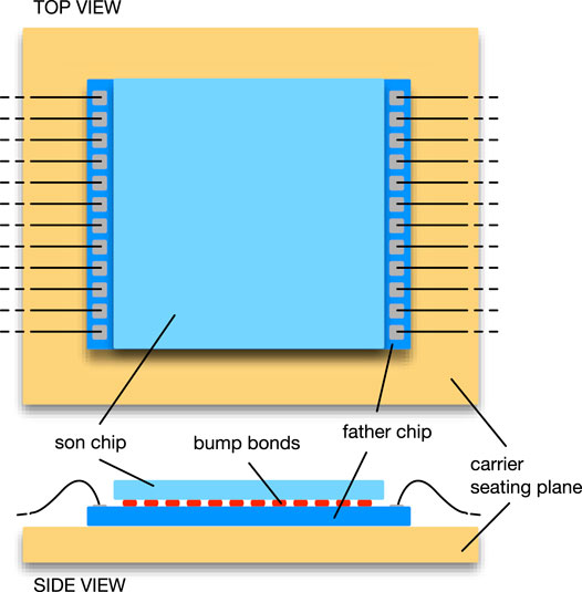
FIGURE 1. Schematic top and side views of the dual layer SPAD array on the carrier seating plane. The dimensions of the chips, of the gap between the chips and of the seating plane, as well as the distance between bonding bumps, are not to scale.
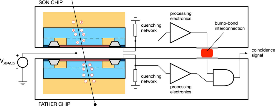
FIGURE 2. Schematic representation of a dual-tier cell with quenching, processing and coincidence circuits. Emphasis is on the coincidence operation of the device. The six metal stack of the technology, and in particular the shielding plate against optical cross-talk between the two chips, are not shown.
The SON and FATHER chips have been fabricated in a 150 nm CMOS technology. They have been designed in such a way that the structures they accommodate can be tested before assembling, in a single-tier configuration. If the difference in size and the additional AND gate in the cells on the FATHER layer are not taken into account, the FATHER chip can be regarded just as a mirror image of the SON chip, so that, when the SON chip is flipped onto the FATHER chip, homologous cells from the two facing sides are connected to each other. Therefore, the independent characterization of FATHER and SON layers is not expected to yield substantially different results. The chips are both subdivided into four different sub-arrays, as schematically shown in Figure 3 in the case of a FATHER chip. The main features of the sub-arrays are described in Table 1. SPADs in sub-array a − 2 are not functional due to a design error. Sub-array a − 4 includes a few different SPAD variants, among which 42 SPAD cells operated with an active quenching technique (the SPAD active area in these latter cells is 70 × 42 μm2, with a FF of 52%).
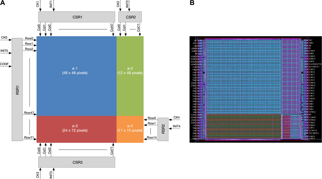
FIGURE 3. Father chip: (A) schematic view of the four sub-arrays, with the shift registers for cell selection and enabling and (B) layout cell view.
The four sub-arrays can be biased separately, in such a way that each sub-array can be characterized with minimum possible interference from the other sub-arrays. A cross section of the SPAD used in all of the four sub-arrays is shown in Figure 4. The SPAD, as anticipated, is based on a p+/n-well junction, with an active volume about 1 μm thick. Isolation from the substrate is obtained by means of a deep n-well (N-iso in the figure), which allows the chip die to be thinned down to a few micron without undermining the sensor functionality [13]. The guard ring is implemented by blocking the n-well, at the border of the junction, with a lowly p-doped ring surrounding the active area, in order to avoid premature edge breakdown [16].
The tests presented in the following were performed on four samples overall: three single layer chips (2 FATHERS, FATHER1 and FATHER2, and one SON) and one dual-layer structure.
SPAD sensors can be individually selected to be enabled or read out. Cells can be selected by means of a set of column (CSRx) and row shift registers (RSRx), located around the four sub-arrays, as illustrated in Figure 3A. The four sub-arrays can be easily identified in the chip layout view, shown in Figure 3B. Each shift register is provided with two input signals, INITx (x = 0,1,2,3,4), used for register initialization, and CKx (x = 0,1,2,3,4), used for column or row selection. As an additional feature, implemented only in the RSR1 register through the CONF signal, six rows in a-1 and three in a-3 can be simultaneously addressed. This results in eight clock pulses being sufficient to scan all the rows in the a-1 and a-3 arrays and enabling, for those arrays, a parallel readout mode. While the cells are enabled individually (or in groups of eight, in the case of a-1 and a-3 in parallel configuration), cell disabling is the result of a global command acting on all the cells in the chip simultaneously.
Together with the SPAD sensing element, each pixel in the sub-arrays also integrates some simple circuits providing a logic pulse with selectable duration to set a local 1-bit memory (a-1, a-3 and a-4) or to increment by one unit the content of a 10-bit register (a-2).
Figure 5A shows the front-end circuit with passive quenching network used in SPADs located in a-1, a-2, a-3 and in part of a-4 on the FATHER chip. In the SON chip, the output of the monostable circuit is directly connected to the pixel memory, with no AND gate in between. All the transistors used in the circuit (including those implementing the logic gates and the monostable block) are core devices, working at VDD = 1.8 V, with the exception of M1, M2 and M3, which are thick gate oxide transistors operated at 3.3 V, generally employed in input/output (I/O) circuits. Use of I/O transistors makes it possible to extend the range of values of the SPAD excess voltage VEX (defined as the SPAD bias voltage VSPAD minus the breakdown voltage VBD) to slightly more than 3.3 V.
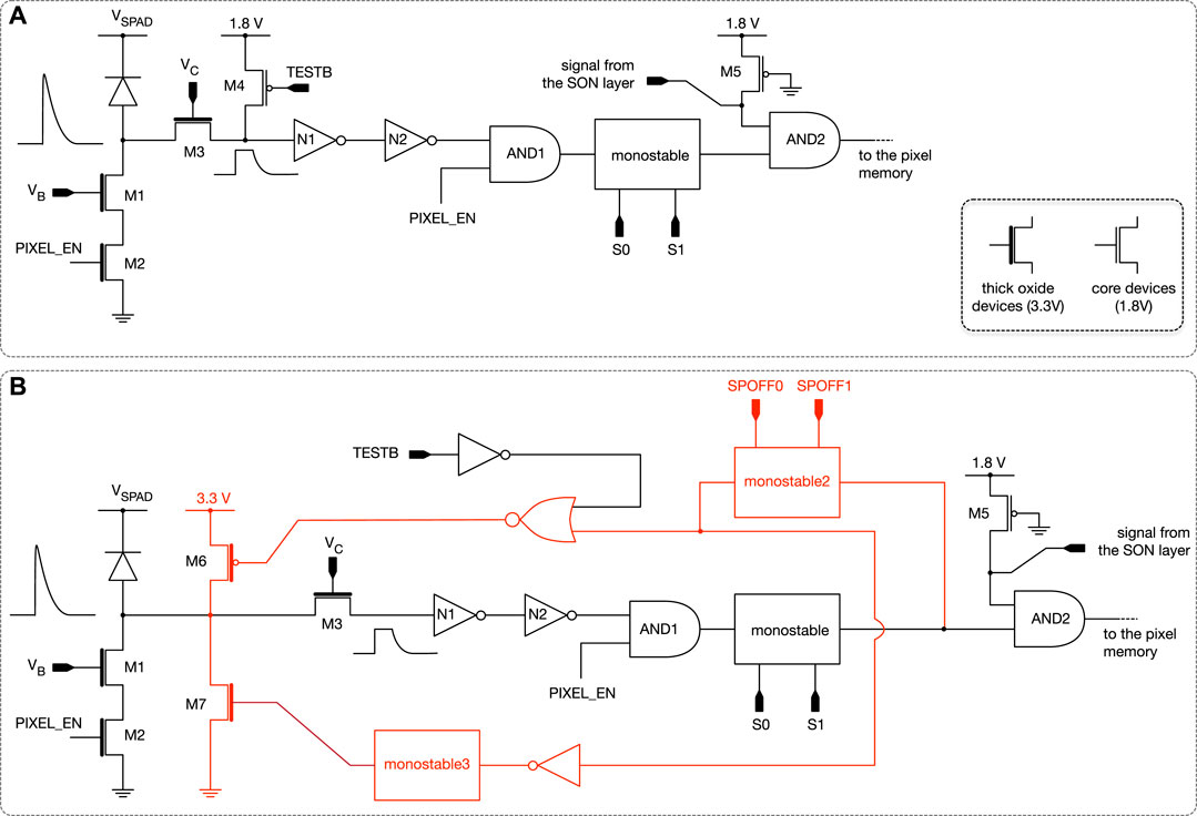
FIGURE 5. Front-end circuits for SPADs in the FATHER chip: (A) with passive quenching network and (B) with active quenching network.
The PIXEL_EN signal, provided by a local programmable latch, is used to control the switch M2 and enable the monostable input. When an avalanche is triggered, transistor M1 switches on and quenches the SPAD current, eventually re-arming the sensor [17]. The voltage pulse at the SPAD anode is the signal to be processed by the circuit. Transistor M3 is used to clip the anode signal to the 1.8 V limit set for core devices. It is followed by a cascaded pair of inverters, the first one featuring a switching threshold around 1 V. This sets to about 1 V the minimum excess voltage needed for a signal to reach the edge-sensitive, monostable block. Depending on the controlling bits S0 and S1, the duration Δt of the signal at the output of the monostable circuit can be nominally set to 400 ps, 750 ps or 2 ns or operated in transparent mode, i.e., with the output node shorted to the input node. In this case, the duration of the pulse at the monostable output corresponds to the time during which the signal from the clipping transistor exceeds the switching threshold of inverter N1. The AND2 gate output provides the coincidence signal between the FATHER and SON layers of the sensor, once the two chips have been assembled. As anticipated, the FATHER chip (and the SON chip as well) can be characterized also in a single-layer configuration. In this case, the M5 pull-up transistor shorts one of the two inputs of AND2 to VDD, therefore making the gate transparent to the signal coming from the monostable (apart from a negligible delay possibly introduced by the gate itself). The signal at the gate output is in the end latched into the local memory cell, or used to increment the content of a counter in the case of the pixels in a-2. The M4 pull-up transistor, controlled by the active low, TESTB signal, is used to emulate a signal coming from the SPAD and check the channel functionality. In order to test the channel with the TESTB signal, the pixel must be enabled and the SPAD operated below the breakdown voltage, so to guarantee that no avalanche can be generated.
Figure 5B shows the front-end circuit with active quenching network for pixels in part of the a-4 array, again in the case of the FATHER chip. In the corresponding SPADs on the SON layer, the output of the monostable directly drives the local 1-bit memory cell. This circuit consists of the front-end with passive quenching network of Figure 5A with the addition of a few blocks, in a red color in Figure 5B, implementing an active quenching technique. The main purpose of active quenching methods is that of mitigating afterpulsing phenomena [18] in avalanche diodes by controlling the hold-off time of the sensor. After-pulsing may render the SPAD unable to detect a true signal for some time after an avalanche and increase the false alarm rate. In applications to charged particle tracking, either effect might unacceptably degrade the detection efficiency. Note anyway that the 1 μs resolution of the measurement system used for the tests, based on an STM32F051 microcontroller (see next section), is not small enough for an assessment, in the investigated devices, of after-pulsing phenomena, typically taking place on a much shorter time scale. Therefore, no evaluation of after-pulsing rejection capabilities could be carried out in this work for the SPADs with active quenching network. In the circuit in Figure 5B, a signal from the SPAD exceeding the threshold set by inverter N1 will trigger the monostable2 circuit. If TESTB = 1 (recall that TESTB is active low), the signal from monostable2, logically inverted by the NOR gate, will keep the SPAD below its breakdown voltage by keeping the transistor switch M6 closed. The hold-off time will depend on the duration Δtʹ of the signal at the monostable2 stage output. Δtʹ, set by means of the SPOFF0 and SPOFF1 bits, can range from 70 to 130 ns in steps of 20 ns. The falling edge of the signal at the output of the monostable2 circuit in turn triggers the monostable3 block, whose output signal, controlling the gate of the M7 transistor, helps restore the SPAD operation after the hold-off interval.
In this paper, a set of three FATHER and SON chips in a single layer configuration and a dual layer chip have been characterized in terms of DCR. DCR measurements were also used to extract information about breakdown voltage for SPADs in single chips. A schematic representation of the measurement setup is shown in Figure 6. The DUT carrier is soldered on a daughterboard, which in turn is mounted on a motherboard. In this way, different DUTs can be tested using a single motherboard. This pair of PCBs serves as an interface between the DUT and the external instrumentation for device powering, biasing, configuration and probing. A PC, running the whole setup through a MATLAB® script, communicates with an STM32F051 microcontroller through a bluetooth connection, and with an Agilent E3631A power supply unit, biasing the SPAD sensors, by means of a GPIB interface. In this way, the system can automatically perform a full DCR characterization of an entire chip with no need for any external action before the process has been completed. By changing the voltage generated by the power supply unit, DCR measurements can be repeated at different SPAD excess voltage. All of the analysis is carried out offline in the Matlab environment.
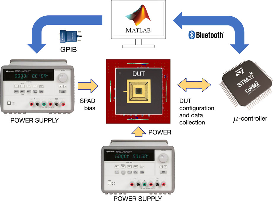
FIGURE 6. Schematic representation of the measurement setup used for DCR characterization of the DUTs.
As anticipated, the measurements shown in this paper have been performed both on single-layer and dual-layer SPAD arrays. DUT characterization has been carried out at a temperature of 25°C, with fluctuations of ±0.5°C around this value.
Figure 7 shows the dark count rate as a function of the voltage applied to the SPAD cathode, VSPAD, for three different pixels from the a-1 array in a single-layer FATHER chip. The DCR counts were accumulated in an integration time of a few hundred of ms. The front-end channel, which, for sensors in the a-1 array (and in a-3 array as well) is the circuit in Figure 5A, can detect an avalanche pulse only when the cathode voltage exceeds the SPAD breakdown voltage plus the threshold voltage of inverter N1, set by design to about 1 V. The same is true for the front-end circuit in Figure 5B. This provides a justification for the step-like shape of the curves.
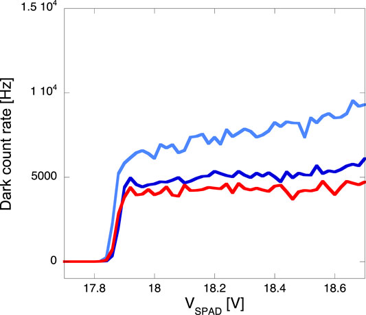
FIGURE 7. Dark count rate as a function of the voltage applied to the SPAD cathode for three different pixels from the a-1 array in a FATHER chip (FATHER1).
Based on the above considerations, for each pixel, the breakdown voltage has been extracted by subtracting the N1 inverter threshold voltage from the voltage at which the DCR vs

FIGURE 9. Breakdown voltage distribution for pixels from three a-1 structures (figures (A),(B)) and for pixels from a-3 and a-4 structures (figures (C),(D)) in single-layer FATHER and SON chips.
Figure 10 shows the DCR cumulative distribution for SPADs from different array structures in single-layer FATHER and SON chips. For all the curves in the figure, the DCR was measured at an excess voltage of 1.7 V, the excess voltage being here defined, for each array, as the difference between the voltage applied to the SPAD cathode and the average value of the breakdown voltage. In the case of the SPAD cells with active quenching network (belonging to the a-4 array), the hold-off time was 70 ns. The staircase-like shape of the relevant distribution is due to the relatively small number of samples (as already mentioned, 42) available in the a-4 array. The cumulative distribution curves cover approximately a couple of decades in DCR values. In the figure, between brackets, the median value of the DCR is also indicated for each distribution. It goes from a few kHz (about 2.3 Hz/μm2) for the SPADs with the smallest active area (those in the a-3 array) to about 7 to 8 kHz (around 1.9 to 2.1 Hz/μm2) in the sensors with the largest active area (the SPADs in the a-1 arrays).
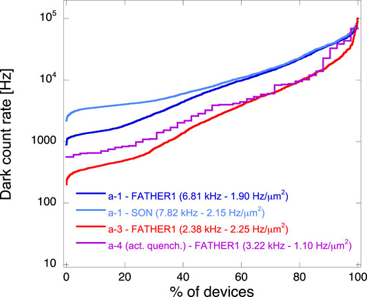
FIGURE 10. DCR cumulative distribution curves for pixels from different array structures in different single-layer samples.
Figure 11 shows the coincidence DCR cumulative distributions for pixels from an a-1 array in a bi-layered chip. The distributions were obtained for different values of the SPAD bias voltage, from 20 to 21 V with 200 mV steps. The coincidence window, i.e., the duration of the signal at the output of the monostable block in the front-end circuit of Figure 5A, was 2 ns. The median DCR relevant to each curve is also indicated between brackets in the figure. As expected, very small values, as compared to those in Figure 7, were detected, ranging from about 0.21 Hz (about 60 μHz/μm2) at
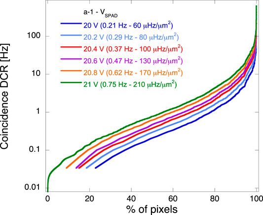
FIGURE 11. Coincidence DCR cumulative distribution curves for pixels from an a-1 structure in a dual-layer sample. The curves were obtained for different values of the bias voltage applied to the SPADs. The coincidence window duration is 2 ns.
Figures 12A–C show the coincidence DCR cumulative distribution for pixels from an a-1, an a-3 and an a-4 array in a bi-layered sample, taken at
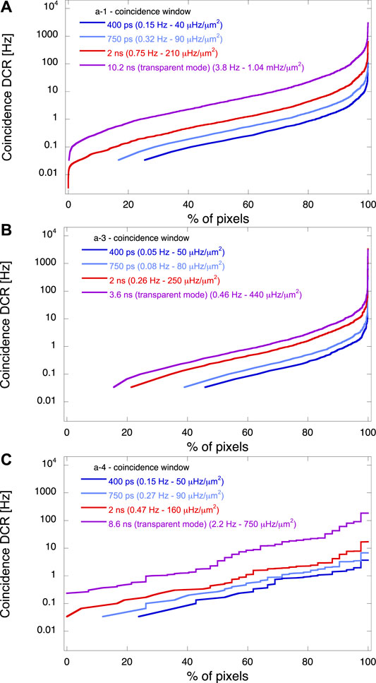
FIGURE 12. Coincidence DCR cumulative distribution curves for pixels in a dual-layer sample from (A) an a-1, (B) an a-3 and (C) an a-4 array. In each figure, the curves were measured at different values of the coincidence window width.
The random occurrence of avalanche current pulses in a PN silicon junction biased above the breakdown voltage, which defines the DCR performance of a SPAD sensor, is mainly ruled by trap-assisted thermal generation of non-equilibrium carriers in the depleted layer. Direct thermal generation in the bulk of minority carriers diffusing to the avalanche multiplication region usually provides a negligibly small contribution to the overall dark count rate [19]. Band-to-band tunneling mechanisms may come into play for large enough electric field strength in the depleted region [20]. DCR also tends to grow with the excess voltage, due to the increase in the avalanche triggering probability and to field-enhanced generation mechanisms [21, 22]. This is in agreement with the results shown in the previous section, where an overall monotonic increase with the voltage applied to the SPAD cathode is always detected, both in individual SPAD characterization (Figure 7) and in cumulative distribution measurements in single and dual-layer devices (Figures 10–12). In the case of a sensor made up by two spatially overlapping and interconnected SPADs, set up to produce a coincidence signal, the probability of two random avalanche events taking place in the two SPADs within a time window
Application of the statistical rules for compound probabilities and independent probabilities [23] leads for the coincidence dark count rate
where
Figure 13 shows the DCR cumulative distribution for SPADs from a-1 arrays in a SON and a FATHER chip. The two curves were obtained at a SPAD bias voltage of 18.4 V. SPADs in the two chips were therefore biased at the same voltage, as in the case they were bonded together to form a dual-layer sensor, although this choice results in a different excess voltage for the pixels on the two dice (featuring two different average breakdown voltages, see Figure 9). Again in Figure 13, an estimate of the coincidence DCR distribution, obtained from the two sets of DCR measurements leading to the two single-layer curves, is displayed (dashed line with triangle markers). A coincidence window duration of 2 ns was considered. In order to construct the estimated distribution, SPADs from the a-1 array in the SON chip were randomly paired with SPADs from the a-1 array in the FATHER chip. This pairing operation was repeated on the entire arrays several times in a series of Monte Carlo runs, yielding a set of curves with negligible difference among each other. From this set, the curve in the figure has been selected as a representative element. For the sake of comparison, the coincidence DCR cumulative distribution measured for SPADs from an a-1 array in a dual-layer structure is also shown in Figure 13. The cumulative distribution displayed here is the one taken at a bias voltage of 20 V and with a coincidence window of 2 ns, already shown in Figure 11. No preliminary breakdown voltage measurement was performed on the two chips making up the dual layer structure. However, the agreement between the estimated curve, obtained, as already mentioned, from SPADs biased at 18.4 V, and the one resulting from the dual-layer structure characterization, with SPAD biased at 20 V, may be an indication of the fact that at least one of the two chips in the assembled sensor features a larger breakdown voltage than the two single-layer chips. This is compatible with the experimental data shown in Figure 9, where SPADs from the a-1 and a-3 arrays in one of the FATHER chips exhibit an average breakdown voltage in excess of 18 V. This has to be compared to the 16 and 16.7 V average breakdown voltage exhibited by a-1 arrays in the SON and the FATHER1 chips respectively.
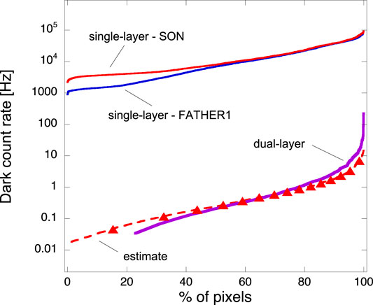
FIGURE 13. Estimated coincidence DCR cumulative distribution for a dual-layer a-1 array obtained from two single-layer distributions. A comparison with the coincidence DCR cumulative distribution from a dual-layer structure is proposed. The coincidence window duration is 2 ns.
In Figure 14, the median coincidence DCR, extracted from the curves of Figures 12A–C, is plotted as a function of
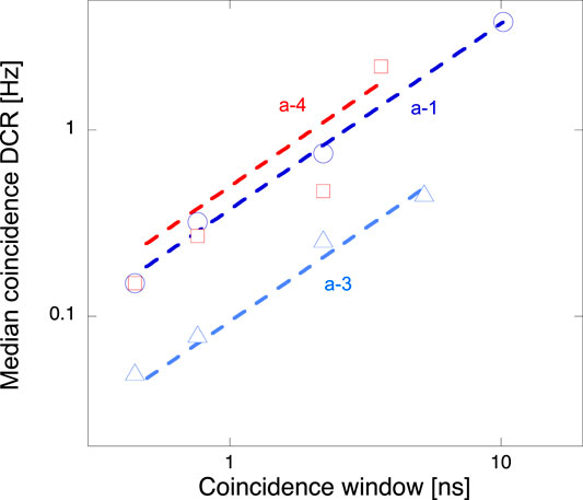
FIGURE 14. Median value of the coincidence DCR extracted from cumulative curves relevant to a-1, a-3 and a-4 arrays, plotted as a function of the coincidence window width. Linear interpolation of the data is represented by the dashed lines. The coincidence window width is the one obtained from simulation in typical conditions (typical process corner, 25°C and 1.8 V bias voltage). Note that both axes are in logarithmic scale.
Corner simulations were also performed on the front-end circuit to evaluate the effect of process, bias voltage and temperature variations on the duration of the signal at the monostable output and, as a consequence, on the coincidence DCR. All possible combinations of the following corners were considered:
• process corners: typical, slow nmos/slow pmos (ss), slow nmos/fast pmos (sf), fast nmos/fast pmos (ff), fast nmos/slow pmos (fs);
• temperature corners: 25°C (typical), −20°, 80°C;
• bias voltage: 1.8 V (typical), 1.8 V + 10%, 1.8 V–10%.
Pretty large variations around the signal duration obtained in typical conditions,
To conclude, this work has reported on the characterization of SPADs fabricated in a commercial 150 nm CMOS technology. The chips have been designed to be assembled into a dual-layer structure for coincidence measurements. As compared to previously published data.
• for the first time results from the test of a bi-layered SPAD based on a p+/n-well junction are presented,
• availability of larger SPAD arrays, with a number of cells well in excess of 103, is leveraged to improve the reliability of the statistical parameters extracted from the measurements,
• a more complete characterization of the bi-layer, coincidence approach is achieved through the evaluation of SPADs with different active area and based on different quenching architectures.
Both single-layer and dual-layer devices were characterized from the standpoint of breakdown voltage and dark count rate. The measurement results are consistent with the DCR performance improvement expected from the dual-layer architecture and are comparable with the performance of dual-tier SPADs with p-well/deep n-well structure. Possible advantages that this approach can ensure in terms of tolerance to ionizing and non-ionizing radiation might be worth investigating. The study of radiation-induced effects in single- and dual-tier devices may also shed some light on the mechanism underlying DCR performance degradation in irradiated SPADs. Finally, DCR tests at different temperatures are being planned, together with the design of a faster, FPGA-based measurement setup for full characterization of the cells with active-quenching network.
The raw data supporting the conclusions of this article will be made available by the authors, without undue reservation.
PM, LP, and G-FDB further developed the idea, already proposed in the literature, of a dual-layer SPAD sensor and devised a procedure for its fabrication. LR and CV (together with Marco Musacci, whose contribution is acknowledged) designed the chips characterized in this work. G-FDB, PM and LP interacted with the company taking care of chip assembly. PB and AS took care of chip bonding and packaging. CV and GT designed and set up the measurement system. GT characterized the DUTs. LR, GC, LP, and GT took care of data analysis. LR wrote the manuscript. Everybody reviewed it.
The activity leading to the results presented in this paper was carried out in the framework of the ASAP project, funded by the Italian Institute for Nuclear Physics (INFN).
The authors declare that the research was conducted in the absence of any commercial or financial relationships that could be construed as a potential conflict of interest.
The authors are indebted to Marco Musacci, who designed the chips that were characterized for this work.
1. Degerly Y, Bortolone G, Claus G, Dorokov A, Dulinski W, Goffe M, et al. A digital monolithic active pixel sensor chip in a quadruple-well CIS process for tracking applications. IEEE Trans Nucl Sci (2013) 60:3899–906. doi:10.1109/TNS.2013.2280794
2. Hara K, Shinsho K, Ishibashi T, Arai Y, Miyoshi T, Ikemoto Y, et al. Development of FD-SOI monolithic pixel devices for high-energy charged particle detection. In: IEEE nuclear science symposium conference record; 2011 Oct 23–29; Valencia, Spain. New York, NY: IEEE. p. 1045–50. doi:10.1109/NSSMIC.2011.6154318
3. Peric I. A novel monolithic pixelated particle detector implemented in high-voltage CMOS technology. Nucl Instrum Methods (2013) 582:876–85. doi:10.1016/j.nima.2007.07.115
4. Kushpil S, Krizek F, Isakov A. Recent results from beam tests of the ALPIDE pixel chip for the upgrade of the ALICE inner tracker. IEEE Trans Nucl Sci (2019) 66:2319–23. doi:10.1109/TNS.2019.2945234
5. Niclass C, Soga M, Matsubara H, Ogawa M, Kagami M. A 0.18 μm CMOS SoC for a 100-m-range 10-frame/s 200 × 96-pixel time-of- flight depth sensor. IEEE J Solid State Circ (2014) 49:315–30. doi:10.1109/JSSC.2014.2364270
6. Popleteeva M, Haas KT, Stoppa D, Pancheri L, Gasparini L, Kaminski CF, et al. Fast and simple spectral flim for biochemical and medical imaging. Optic Express (2015) 23:23511–25. doi:10.1364/OE.23.023511
7. Braga LHC, Gasparini L, Grant L, Henderson RK, Massari N, Perenzoni M, et al. A fully digital 8 × 16 SiPM array for PET applications with per-pixel TDCs and real-time energy output. IEEE J Solid State Circ (2014) 49:301–14. doi:10.1109/JSSC.2013.2284351
8. Kostamovaara J, Tenhunen J, Kögler M, Nissinen I, Nissinen J, Keränen P. Fluorescence suppression in Raman spectroscopy using a time gated CMOS SPAD. Optic Express (2013) 21:31632–45. doi:10.1364/OE.21.031632
9. Vilella E, Alonso O, Diéguez A. 3D integration of Geiger-mode avalanche photodiodes aimed to very high fill-factor pixels for future linear colliders. Nucl Instrum Methods (2013) 731:103–8. doi:10.1016/j.nima.2013.05.022
10. Pancheri L, Ficorella A, Brogi P, Collazuol G, Dalla Betta GF, Marrocchesi PS, et al. First demonstration of a two-tier pixelated avalanche sensor for charged particle detection. IEEE J. Electron Devices Society (2017) 5:404–10. doi:10.1109/JEDS.2017.2737778
11. Ratti L, Brogi P, Collazuol G, Betta GFD, Ficorella A, Marrocchesi PS, et al. DCR performance in neutron-irradiated cmos spads from 150- to 180-nm technologies. IEEE Trans Nucl Sci (2020) 67:1293–301. doi:10.1109/TNS.2020.2978198
12. Alonso O, Casanova R, Dieguez A, Dingfelder J, Hemperek T, Kishishita T, et al. Depfet active pixel detectors for a future linear e+e− collider. IEEE Trans Nucl Sci (2013) 60:1457–65. doi:10.1109/TNS.2013.2245680
13. Pancheri L, Brogi P, Collazuol G, Dalla Betta GF, Ficorella A, Marrocchesi P, et al. First prototypes of two-tier avalanche pixel sensors for particle detection. Nucl Instrum Methods (2017) 845:143–6. doi:10.1016/j.nima.2016.06.094
14. Ficorella A, Pancheri L, Brogi P, Collazuol G, Dalla Betta GF, Marrocchesi PS, et al. Crosstalk characterization of a two-tier pixelated avalanche sensor for charged particle detection. IEEE J Sel Top Quant Electron (2018) 24:3801108. doi:10.1109/JSTQE.2017.275511
15.ATLAS. Technical design report for the ATLAS inner tracker pixel detector. Tech. Rep. CERN-LHCC-2017-021. ATLAS-TDR-030. Geneva, Switzerland: CERN (2017).
16. Pancheri L, Stoppa D. Low-noise single photon avalanche diodes in 0.15 μm CMOS technology. In: 2011 Proceedings of the european solid- state device research conference; 2011 Sep 12–16; Helsinki, Finland. New York, NY: IEEE. p. 179–82.
17. Dalla Betta GF, Pancheri L, Stoppa D, Henderson R, Richardson J. Avalanche photodiodes in submicron cmos technologies for high-sensitivity imaging. In: GF Dalla Betta, editor. Advances in photodiodes. London, UK: IntechOpen (2011). p. 225–48.
18. Cova S, Ghioni M, Lacaita A, Samori C, Zappa F. Avalanche photodiodes and quenching circuits for single-photon detection. Appl Optic (1996) 35:1956–76. doi:10.1364/AO.35.001956
19. Xu Y, Xiang P, Xie X. Comprehensive understanding of dark count mechanisms of single-photon avalanche diodes fabricated in deep sub-micron CMOS technologies. Solid State Electron (2017) 129:168–74. doi:10.1016/j.sse.2016.11.009
20. Ghioni M, Gulinatti A, Rech I, Zappa F, Cova S. Progress in silicon single-photon avalanche diodes. IEEE J Sel Top Quant Electron (2017) 13:852–62. doi:10.1109/JSTQE.2007.902088
21. McIntyre RJ. A new look at impact ionization - Part I: a theory of gain, noise, breakdown probability, and frequency response. IEEE Trans Electron Dev (1999) 46:1623–31. doi:10.1109/16.777150
22. Martin PA, Streetman BG, Hess K. Electric field enhanced emission from non-coulombic traps in semiconductors. J Appl Phys (1981) 52:7409–15. doi:10.1063/1.328731
Keywords: SPAD, CMOS, DCR, charged particle detection, dual layer
Citation: Ratti L, Brogi P, Collazuol G, Dalla Betta G-F, Marrocchesi PS, Pancheri L, Sulay A, Torilla G and Vacchi C (2021) Layered CMOS SPADs for Low Noise Detection of Charged Particles. Front. Phys. 8:607319. doi: 10.3389/fphy.2020.607319
Received: 16 September 2020; Accepted: 30 November 2020;
Published: 14 January 2021.
Edited by:
Paul Sellin, University of Surrey, United KingdomReviewed by:
Horst Zimmermann, Vienna University of Technology, AustriaCopyright © 2021 Ratti, Brogi, Collazuol, Dalla Betta, Marrocchesi, Pancheri, Sulay, Torilla and Vacchi. This is an open-access article distributed under the terms of the Creative Commons Attribution License (CC BY). The use, distribution or reproduction in other forums is permitted, provided the original author(s) and the copyright owner(s) are credited and that the original publication in this journal is cited, in accordance with accepted academic practice. No use, distribution or reproduction is permitted which does not comply with these terms.
*Correspondence: Lodovico Ratti, bG9kb3ZpY28ucmF0dGlAdW5pcHYuaXQ=
Disclaimer: All claims expressed in this article are solely those of the authors and do not necessarily represent those of their affiliated organizations, or those of the publisher, the editors and the reviewers. Any product that may be evaluated in this article or claim that may be made by its manufacturer is not guaranteed or endorsed by the publisher.
Research integrity at Frontiers

Learn more about the work of our research integrity team to safeguard the quality of each article we publish.