 Jiangtao Su
 Jianhua Wang
- Key Laboratory of RF Circuits and Systems, Ministry of Education, HangZhou, China
In this paper, the uncertainty and the impact of imperfect load calibration standard for on-wafer Through-Reflect-Match calibration method are analyzed with the help of 3D electromagnetic simulations. Based on the finding that load impedance can lead to significant errors in calibration, an automatic algorithm to determine the complex impedance of the load standard is proposed. This method evaluates the resistance as well as the parasitic inductance introduced by the misalignment of the probe tip to the substrate pad at mm-wave frequencies or the non-precize load standard. The proposed algorithm was verified by practical measurement, and the results show that by incorporating actual load impedance into the calibration algorithm, the deviations of RF measurement results are greatly suppressed.
1 Introduction
In order to research and develop the application of millimeter wave devices in the commercial world, accurate on-wafer measurement is a key requirement since it eliminates the additional errors and uncertainties introduced by the device package [1–3]. For this purpose, careful on-wafer calibrations must be employed to eliminate the systematic errors typically caused by system directivity, loss/delay of measurement paths, or the mismatch of measurement ports. The calibration process of determining error coefficients involves the measurement of a set of pre-defined calibration standards, and various calibration algorithms have been developed and named according to the types of calibration standards being used [4]. Those standards are assumed to have either known or partially known “ideal” characteristics. However, at higher frequencies, due to the difficulty in manufacturing precise calibration standards, it is widely accepted that TRL calibration, which consists of measuring Through, Reflect, and Transmission Line standards, is the most accurate method since it has the least requirement for precise calibration standards and lumped models [5].
However, the TRL technique sets the reference impedance after the calibration by the characteristic impedance of the through/lines used. The accurate determination of the frequency-dependent calibration lines’ characteristic impedance thus becomes a key requirement to allow for the correct S-parameter measurement. At lower frequencies, when radiation losses and surface waves can be neglected, the line’s characteristic impedance can be calculated using quasi-static approaches like con-formal mapping [6–8]. But with the frequency increasing and the substrate becoming complex, these become less accurate. Many techniques have since been proposed to solve this issue, such as extracting from S-parameter measurements [9], estimating from capacitance per unit length [10], using 3D EM simulation to estimate transmission line impedance [11], or relating the characteristic impedance of the line to an ideal pure-real load [12, 13].
The issue of accurate characteristic impedance of lines, along with other shortcomings of TRL calibration, such as how multiple lines are required to cover greater than an 8:1 frequency band and the impractically long length of lines at lower frequencies, calls for an alternative calibration approach to TRL calibration [14, 15]. Recently, the Through-Reflect-Match (TRM) method has shown the potential to be widely used in on-wafer measurement [16, 17]. TRM is very similar to TRL calibration in that it does not require accurate specification of the reflect standard coefficient. However, unlike TRL calibration, the through standards must be a non-zero length through (line). Additionally, the perfect match standard is substituted for the line standard in the TRL method, which in practical terms can be conceived as an infinitely long line. In TRM calibration, the match standard is the only impedance that needs to be defined. Moreover, the reflect needs only to be identical for each port so that a fixed-size well-behaved coplanar resistor is enough for broadband and accurate on-wafer measurement systems [18, 19].
However, the biggest problem with TRM calibration is its reliance on a precise and predictable load standard. When the assumption of a non-reflecting match standard is not fulfilled, calibration introduces extra residual errors, which degrades the measurement accuracy. However, the ideal load standard to provide a perfect match can never be realized in practice [20] Moreover, due to the overlap between the probe tip and the calibration pad, parasitic load inductance also rises. The accurate determination of the load impedance thus becomes a key requirement of TRM calibrations, and the actual value of the match standard must be incorporated into the calculation of the error coefficients. Many researchers have noticed this issue, and several complex algorithms to estimate and to correct the effect of the load reactance have been proposed [21–23]. These methods still have the assumption that the resistance of the load is frequency independent and has the same impedance with the thru lines. Other reported techniques include using precisely known frequency-dependent load [17, 24] or using LRRM methods [25] and TMRR [26] to overcome the inaccuracy of the match standard.
In this paper, we propose an improved method to characterize the imperfect match standard for precise on-wafer TRM calibration. Firstly, an uncertainty analysis of TRM calibration using imperfect calibration standards is carried out. Next, a model of the load standard is established using 3D EM simulation. A smart automatic load impedance determination algorithm is thus elucidated. Finally, in section 4, the proposed method is verified on a real on-wafer measurement bench, showing the effectiveness of this method.
2 Uncertainty Analysis of TRM Calibration
A simplified block diagram of an on-wafer measurement system is shown in Figure 1A, where the main instruments used are a probe station and a Vector Network Analyser (VNA) and its simplified error network can be expressed as in Figure 1B. If the isolation and non-symmetry between the non-measurement ports can be dismissed, the standard 16-term error model can be simplified to a standard eight-term error model, where e00,e11,e01, and e10 are the error terms of block A, and e22,e23,e23, and e32 are error terms of bock B. The calibration process can thus be inferred to determine the eight error terms from a set of uncorrected S-parameters measured on a set of calibration standards. For a two-port network, the S-parameter Sij of calibration items are therefore linearly related to the raw S-parameter measurement data by error terms e00e32. For TRM calibration, the raw S-parameter measurement data measured by the Vector Network Analyzer can be expressed as
where
In order to evaluate the measurement deviations
By Eq. 8, the deviations of measurement S parameters,
In the above equations, the Rm, Tm, and Mm correspond to the measured S parameters of the Reflect, Thru, and Match standards, respectively. In the scenario that the calibration standards are not ideal, the deviations of the S parameters are calculated as
In the above equations, the Rm, Tm, and Mm correspond to the measured S parameters of the Reflect, Thru, and Match standards respectively. In the scenario that the calibration standards are not ideal, the deviations of the S parameters are calculated as follows.
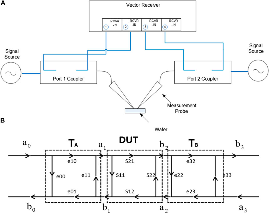
FIGURE 1. Typical on-wafer measurement system structure: (A) Topology diagram and (B) Simplified error network diagram.
For non-ideal Reflection standard:
For non-ideal Thru standard:
For non-ideal Match standard:
The above analysis suggests that the non-ideal reflect standard does not affect the measured reflection coefficient, whilst the deviation of the through and match standards would cause degradation of the measured impedance and insertion loss. In other words, the errors in the TRM calibration mainly come from the asymmetry of a through/line standard and the deviation of the load standard from 50 Ω.
The error comes from the first source and can be minimized by introducing an additional reverse injected active VNA measurement as proposed in Ref. 18, but the latter has to rely on perfect fabrication of load standard or accurate characterizing the load impedance. However, the impedance of most on-wafer loads is non-ideal; it is not only limited by the fabrication process but could also contribute to the variation in environment temperature. This would lead to significant error in the subsequent measurement, especially in mm-wave and further high-frequency bands. It is therefore necessary to characterize the actual load impedance and incorporate them to TRM calibration.
3 Determine the on-Water Load Impedance
3.1 Model of the Match Standard
For on-wafer measurement, the calibration standard is typically fabricated in the form of coplanar waveguide (CPW) geometry. As shown in Figure 2, the load consists of two 100 Ω resistors in between the Ground-Signal-Ground (GSG) pads, which are typically made of thin film gold to connect with the probe tips. Figure 2 also shows the real image of a typical microscope view of the load standard under the probe station. Because the probe tip is fragile, the connection between the probe tip and the calibration standards may vary during different measurements. Moreover, since the probe position to the pad relies wholly on the operators’ manipulation under microscopic observation, the contact point between the probe tips and the pads may differ from one measurement to another. Usually for high-frequency measurement, the complete calibration measurement must be iterated several times before acceptable measurement results are obtained.
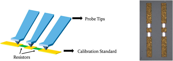
FIGURE 2. The full structure including probes, pad and calibration standard (left), and the microscope view of a real load standard (right).
To better understand the influence of the probe-pad alignment on the load impedance, EM simulation using HFSS software was carried out. In the simulation, the meshed ground planes were simplified considering a continuous metal connection, both vertically and horizontally. This simplification provides a good approximation of the electrical response of the structure, the openings in the metal mesh being much smaller than the wavelength. The signal pad is modeled as a 50*50*3.4 um metal with conductivity of 4.9E7 S/m, and the distance from the signal pad to ground is 100 um. The load consists of two identical zero-thickness rectangular sheets in contact with the signal pad and the ground with a boundary condition of 100 lumped resistance. The CPW line is excited by a wave-guide port considering parasitic effects.
Figure 3 provides the electric field distribution at the wave feeding port, indicating a gentle discontinuity when load resistance is present. This mainly comes from the simulation process where resistance presents a large topological discontinuity, and the boundary conditions therefore lead to the numerical solution deviations in the finite-element numerical simulation process. Figure 4 shows that by putting the probe tip at three different positions 40 um apart, a non-negligible deviation in the impedance emerges, which indicates a possible source of calibration error.
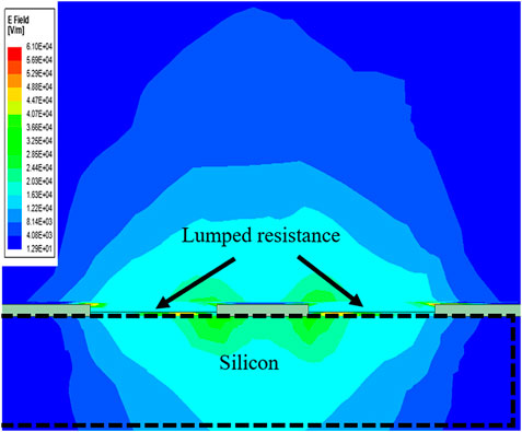
FIGURE 3. Field distribution of match standard at 100 GHz simulated by Ansoft HFSS Software.
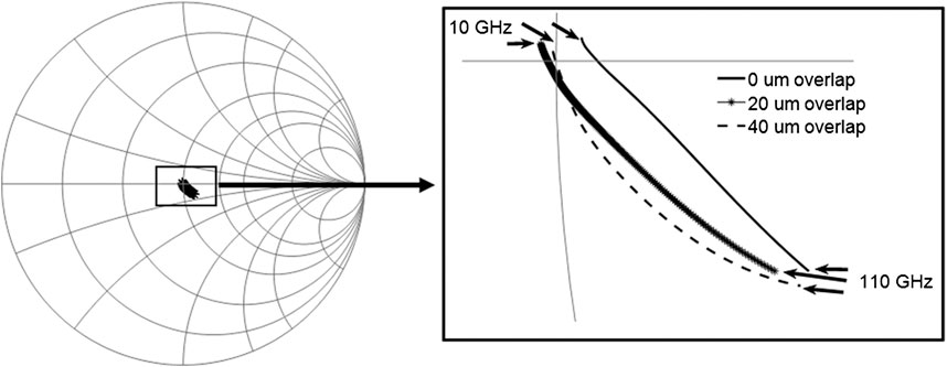
FIGURE 4. The variation of match standard impedance with different probe tip position on pads.
A lumped elements model, as shown in Figure 5, was constructed to further analyse the impedance of the match standard, which takes account of the distributed nature of the load, as well as the coupling between the probe and the calibration standard. During the measurement, the capacitance across the resistor stayed nearly constant, but the inductance changed significantly due to the change of probe tip contact position. Since the capacitance was very small and can be regarded as negative inductance, a simplified first order inductance in series with the resistor, also as shown in Figure 5, can be used to simplify the analysis. It is also worth noting that the value of this inductance now includes different probe contacts between different measurements.
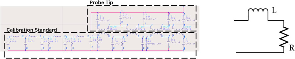
FIGURE 5. The lumped circuit model for probe contacting with the calibration standard in ADS simulation software (left) and simplified equivalent circuit model (right).
As can be seen in Figure 6, the simplified model accounts for the DC resistance of the load and the series inductance fits well with the complicated mis-alignment model and the EM simulation. It is therefore possible to use the simplified model alone to determine the resistance and inductance of the load.
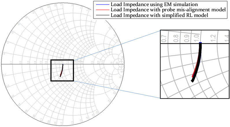
FIGURE 6. The load impedance using EM simulation, probe misalignment model and simplified model.
3.2 Evaluation of Actual Match Impedance
From the analysis in section 2, if the TRM calibration is performed with the assumption that the match is ideal, while in reality it is not, an offset will be introduced into the measured DUT impedance. Supposing the load has an actual impedance of
The TRM calibration method, by definition, always solves the error terms with the reference plane at the center of the Through standard. The probes-in-air open therefore actually corresponds to a negative-length open stub with a length one-half that of the Through standard and with the reflection coefficient magnitude of unity. If the match standard used in the calibration is offset, it would appear to have a magnitude different from one; additionally, as the on-wafer ISS short standard typically has the same length as the Through line, the short standard will have the reflection coefficient magnitude of unity but in the admittance chart. The open and short calibration standard thus provides a convenient means of determining how far the match standard is offset from the standard 50 Ω.
Returning to the calibration models described in Figure 1, supposing the same match standard is used in both port 1 and port 2 measurement, the complete measurement matrix of TA can be represented as
ZM represents the impedance of the loads used as the match standard at measurement port. The terms
As the KA is solely decided by the match standard, for one port, DUT is measured at port 1, Eq. 16 is still valid, and the measured Y parameter of the DUT can be expressed as
If the match standard is improperly defined, the above function will behave as
Obviously, the Y parameter of the ideal load and actual load can be separately defined as
Considering the scenario that the DUT is a pure reflection such as an open standard, and combining Eqs 12 and 13, we have
Similarly, considering the DUT is a pure reflection as short standard, we have
According to Eqs 20 and 21, therefore, after TRM calibration, if we have the ideal open and short calibration standard, the correct impedance and inductance of the load can be calculated. However, this algorithm so far still has the assumption that the loss from the probe tip to the center-of-through is 0. Since the length of the Through standard typically is very short, the loss usually is so small that it can be considered negligible. For example, the FormFactor 101-190 ISS calibration standard has a loss of 0.04 dB at 40 GHz. However, at higher frequencies on the mm-Wave band, the Through loss becomes an issue which would make the reflection coefficient of the open/short standard not equal, nor equal to unity, thus rendering the extracted load impedance no longer accurate.
To correct the limitations of the proposed algorithm, an iteration process is thus being introduced, which will take account of the length of the Through and the Short standard. The full calibration steps can thus be summarized as follows:
1.Make a TRM calibration with the assumption that the load standard is ideal 50 Ω impedance.
2.Use the calculated error coefficients to measure the S-parameters of the open and short standard.
3.Calculate the actual impedance of the load standard as the guess value.
4.Recalculate the error terms from the calculated actual load impedance.
5.Re-measure the S parameters of the open, short, and through standard with the corrected error terms.
6.Calculate a difference between the expected reflect coefficient of open, short, and thru standard.
7.Repeat step 3 to step 6 to minimizes the errors and obtain the desired load impedance.
4 Measurement Results of This Calibration Method
In order to validate the method proposed, we built a measurement bench composed of a manual probe station, Cascade Summit 11,000, and a Keysight PNA-X Vector Network Analyser. A detailed photo of the measurement bench is shown in Figure 7. A used FormFactor 101-190 ISS substrate, which was clearly worn and by no means in its best condition, was selected to verify if the proposed method could correct the calibration error from the imperfect calibration standard. The measurement frequency was from 0.1 to 40 GHz. The calibration algorithm was implemented using Python as was the instrument control method.
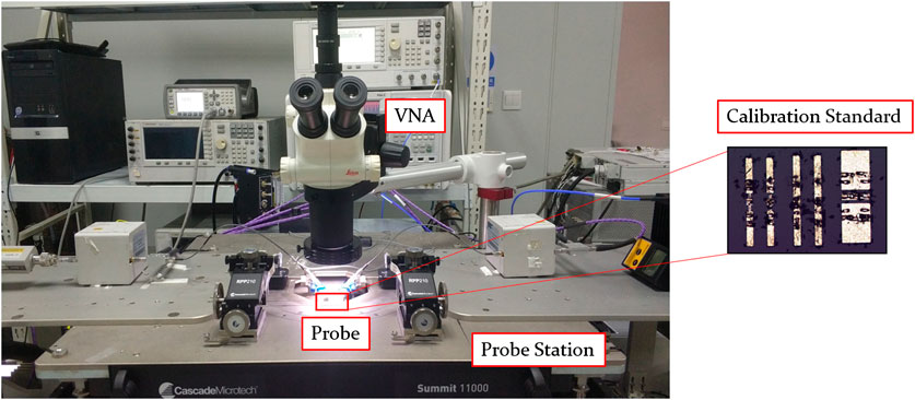
FIGURE 7. The measurement bench and the imperfect calibration standard used in the experiment.
Figure 8 shows the real and imaginary parts of the calculated load impedance extracted using the proposed method. The impedance of the load standard, though perhaps very precise when it was fabricated, is away from 50 and disperses with frequency. This was very probably caused by the worn surface, which can be clearly seen via the microscope, as shown in Figure 7. The dispersion with the frequency also suggests that the parasitic inductance of the load standard changes with the frequency.
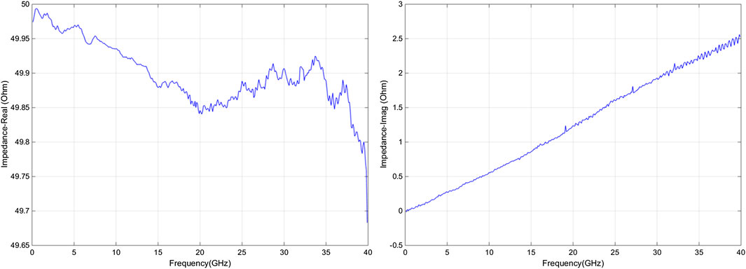
FIGURE 8. The real part of load impedance (left) and the imaginary part of the load impedance (right) calculated load measured.
Next, we drew the S-parameter measurements of the open and short standard, by both the classical TRM calibration method and the impedance correction method proposed in this work. As can be seen in Figure 9 and Figure 10, the ideal probe-on-air open standard has negative inductance, and the short standard is also inductive with the magnitude of unity. Due to the imperfection of the load standard, both the open and short standard are offset from the unity circle using the classical TRM calibration method, which was effectively corrected with the calculated load impedance to recalculate the error coefficients.
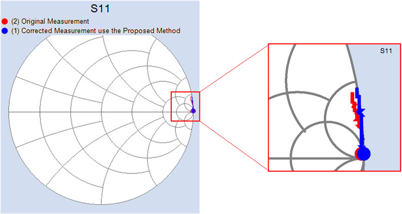
FIGURE 9. The re-measured open standard with conventional TRL calibration method (red) and the correction method proposed in this work (blue).
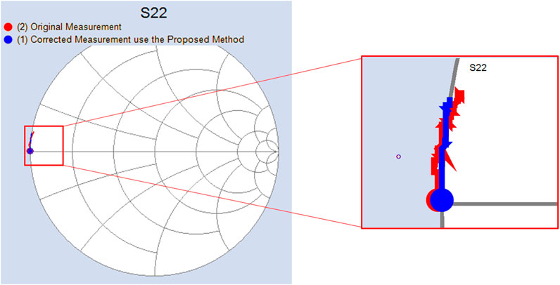
FIGURE 10. The re-measured short standard with conventional TRL calibration method (red) and the correction method proposed in this work (blue).
5 Conclusion
In this paper, a comprehensive analysis of the error source of TRM calibration is presented, leading to the conclusion that load impedance is the most important determinant of on-wafer calibration quality. Based on full wave 3D EM simulations, it is shown that the imperfect load impedance was not only caused by the non-precize DC resistance of the load but also by the overlap between the probe tips and the pads on the substrate.
An improved load impedance estimation algorithm has therefore been presented, which automatically calculates the load’s complex impedance in the calibration process. Actual measurements on worn calibration standards up to 40 GHz show that the RF performance due to the variations of imperfect load standard can be corrected by accommodating the calculated load impedance into the TRM calibration method. The novelty of the estimation method lies in is its immune to pad-to-tip discontinuities since it calculates the actual impedance at the time of calibration. Moreover, the dependence on a fully automated probe station or an operator experienced in on-wafer measurement is eliminated with the proposed smart impedance calculation method. The proposed algorithm would find immediate application in the on-wafer characterization of mm-wave or higher frequencies device.
Data Availability Statement
The raw data supporting the conclusions of this article will be made available by the authors, without undue reservation.
Author Contributions
First Author conceived of the presented idea, JS and JW developed the algorithm and performed the computations. JS and FW. verified the analytical methods with experiment. LS encouraged authors to investigate this calibration issue and supervised the findings of this work. All authors discussed the results and contributed to the final manuscript.
Funding
This work is funded by the National Natural Science Foundation of China (No.61827806, No.61871161) and the Key Lab Research Foundation of Science and Technology on Electronic Test & Measurement Laboratory (6142001190103).
Conflict of Interest
The authors declare that the research was conducted in the absence of any commercial or financial relationships that could be construed as a potential conflict of interest.
References
1. Deng M, Quémerais T, Bouvot S, Gloria D, Chevalier P, Lépilliet S, et al. Small-signal characterization and modelling of 55 nm sige bicmos hbt up to 325 ghz. Solid State Electron (2017) 129:150–6. doi:10.1016/j.sse.2016.11.012
2. Seelmann-Eggebert M, Ohlrogge M, Weber R, Peschel D, Maßler H, Riessle M, et al. On the accurate measurement and calibration of s-parameters for millimeter wavelengths and beyond. IEEE Trans Microw Theor Tech (2015) 63:2335–42. doi:10.1109/tmtt.2015.2436919
3. Yau K, Dacquay E, Sarkas I, Voinigescu SP. Device and ic characterization above 100 ghz. IEEE Microw Mag (2012) 13:30–54. doi:10.1109/mmm.2011.2173869
4. Williams DF, Young AC, Urteaga M. A prescription for sub-millimeter-wave transistor characterization. IEEE Trans Terahertz Sci Technol (2013) 3:433–9. doi:10.1109/tthz.2013.2255332
5. Williams DF, Marks RB, Davidson A. Comparison of on-wafer calibrations. 38th ARFTG Conf Dig (IEEE) (1991) 20:68–81. doi:10.1109/arftg.1991.324040
6. Veyres C, Fouad Hanna V. Extension of the application of conformal mapping techniques to coplanar lines with finite dimensions. Int J Electron (1980) 48:47–56. doi:10.1080/00207218008901066
7. Carlsson E, Gevorgian S. Conformal mapping of the field and charge distributions in multilayered substrate cpws. IEEE Trans Microw Theor Tech (1999) 47:1544–52. doi:10.1109/22.780407
8. Wen CP. Coplanar waveguide: a surface strip transmission line suitable for nonreciprocal gyromagnetic device applications. IEEE Trans Microw Theor Tech (1969) 17:1087–90. doi:10.1109/tmtt.1969.1127105
9. Eo Y, Eisenstadt W. High-speed vlsi interconnect modeling based on s-parameter measurements. IEEE Trans Compon Hybrids Manuf Technol (1993) 16:555–62. doi:10.1109/33.239889
10. Williams DF, Marks RB. Transmission line capacitance measurement. IEEE Microw Guid Wave Lett (1991) 1:243–5. doi:10.1109/75.84601
11. Galatro L, Spirito M. Millimeter-wave on-wafer trl calibration employing 3-d em simulation-based characteristic impedance extraction. IEEE Trans Microw Theor Tech (2017) 65:1315–23. doi:10.1109/tmtt.2016.2609413
12. Marks RB, Williams DF. Interconnection Transmission Line Parameter Characterization. 40th ARFTG Conference Digest, Orlando, FL, USA, 1992. pp. 88–95. doi:10.1109/ARFTG.1992.327004
13. Williams DF, Arz U, Grabinski H. Characteristic-impedance measurement error on lossy substrates. IEEE Micro Wireless Compon Lett (2001) 11:299–301. doi:10.1109/7260.933777
14. Rumiantsev A, Sweeney SL, Corson P.L. Comparison of on-wafer multiline TRL and LRM+ calibrations for RF CMOS applications. 2008 72nd ARFTG Microwave Measurement Symposium, Portland, OR, USA, 2008, pp. 132–136. doi:10.1109/ARFTG.2008.4804291
15. Chen L, Zhang C, Reck TJ, Arsenovic A, Bauwens M, Groppi C, et al. Terahertz micromachined on-wafer probes: repeatability and reliability. IEEE Trans Microw Theory Tech (2012) 60:2894–902. doi:10.1109/TMTT.2012.2205016
16. Eul HJ, Schiek B. Thru-Match-Reflect: One Result of a Rigorous Theory for De-Embedding and Network Analyzer Calibration. 1988 18th European Microwave Conference, Stockholm, Sweden, 1988, pp. 909–914. doi:10.1109/EUMA.1988.333924
17. Doerner R, Rumiantsev A. Verification of the wafer-level LRM+ calibration technique for GaAs applications up to 110 GHz. 65th ARFTG Conference Digest, 2005. Spring 2005, Long Beach, CA, USA, 2005, doi:10.1109/ARFTGS.2005.1500562
18. Su J, Yang B, Gao H, Huang X, Cai J, Wang X, et al. A Novel TRM Calibration Method for Improvement of Modelling Accuracy at mm-wave Frequency. 2018 IEEE/MTT-S International Microwave Symposium - IMS, Philadelphia, PA, 2018, pp. 1300–1303. doi:10.1109/MWSYM.2018.8439263
19. Pulido-Gaytán MA, Reynoso-Hernández JA, Loo-Yau JR, Zarate-de Landa A, del Carmen Maya-Sanchez M. Generalized theory of the thru-reflect-match calibration technique. IEEE Trans Microw Theor Tech (2015) 63:1693–9. doi:10.1109/TMTT.2015.2417860
20. Kirby P, Dunleavy L, Weller T. The effect of load variations on on-wafer lumped element based calibrations. 54th ARFTG Conference Digest, Atlanta, GA, USA, 2000, pp. 1–10. doi:10.1109/ARFTG.1999.327368
21. Davidson A, Jones K, Strid E. Lrm and lrrm calibrations with automatic determination of load inductance. 36th ARFTG Conf Dig (IEEE) (1990) 18:57–63. doi:10.1109/ARFTG.1990.323996
22. Williams DF, Marks RB. Lrm probe-tip calibrations using nonideal standards. IEEE Trans Microw Theory Tech (1995) 43:466–9. doi:10.1109/22.348112
23. Hayden L. An enhanced Line-Reflect-Reflect-Match calibration. 2006 67th ARFTG Conference, San Francisco, CA, USA, 2006, pp. 143–149. doi:10.1109/ARFTG.2006.4734364
24. Scholz RF, Korndorfer F, Senapati B, Rumiantsev A. Advanced technique for broad band on-wafer rf device characterization. In IEEE Arftg 63rd conference. Fort Worth, TX: Spring 2004 (2004). 83–90.
25. Purroy F, Pradell L. New theoretical analysis of the lrrm calibration technique for vector network analyzers. IEEE Trans Instrument Meas (2001) 50, 1307–1314. doi:10.1109/19.963202
Keywords: calibration, on-wafer, vector network measurement, through-reflect-match, load impedance
Citation: Su J, Wang J, Wang F and Sun L (2021) Realization of Accurate Load Impedance Characterization for On-Wafer TRM Calibration. Front. Phys. 8:595732. doi: 10.3389/fphy.2020.595732
Received: 17 August 2020; Accepted: 16 November 2020;
Published: 27 January 2021.
Edited by:
Lin Chen, University of Shanghai for Science and Technology, ChinaReviewed by:
Jianming Wen, Kennesaw State University, United StatesBin Chen, Hefei University of Technology, China
Copyright © 2021 Su, Wang, Wang and Sun. This is an open-access article distributed under the terms of the Creative Commons Attribution License (CC BY). The use, distribution or reproduction in other forums is permitted, provided the original author(s) and the copyright owner(s) are credited and that the original publication in this journal is cited, in accordance with accepted academic practice. No use, distribution or reproduction is permitted which does not comply with these terms.
*Correspondence: Jiangtao Su, anRzdUBoZHUuZWR1LmNu