- State Key Laboratory of Millimeter Waves, School of Information Science and Engineering, Southeast University, Nanjing, China
Spoof surface plasmon polaritons (SPPs) are highly localized surface waves that can be supported on metal surfaces with subwavelength decorations. Mode matching and momentum matching have been investigated so as to efficiently excite the spoof SPPs through conventional planar waveguides (WGs) such as the microstrip (MS) line and the co-planar waveguide (CPW). In this work, a smooth and wideband bridge between the conventional rectangular waveguide and the plasmonic waveguide of spoof SPPs has been proposed and experimentally demonstrated. High efficiency is achieved in both simulation and experiment in a wide frequency range from 12 to 18 GHz. The high-efficiency and broadband excitation of spoof SPPs through rectangular waveguide has great potentials in microwave, millimeter-wave and terahertz circuits, and systems.
Introduction
Surface plasmon polaritons (SPPs) exist on the interface of two media (e.g., metal and the air) with opposite permittivities at optical frequencies [1]. When the electromagnetic (EM) field of incident waves interacts with the plasma of electrons near the surface of the metal, collective oscillations are excited, and propagate along the interface as a special type of surface wave. The SPPs possess some inherent characteristics such as strong confinement of EM field and sub-wavelength resolution, and hence have been developed in surface plasmon-based circuits for the purpose of biosensing, microscopy, extraordinary optical transmissions, near-field optics, etc. [2]. However, at lower frequencies such as terahertz and microwave, metals behave close to perfectly electric conductors (PECs) rather than plasmas. Due to this fact, “spoof” (or “designer”) surface plasmon polaritons, which could be considered as one special type of metamaterials, have been created below the far-infrared frequency so as to obtain the SPP-like dispersion and propagation properties. The spoof SPPs are realized on metallic surfaces with sub-wavelength decorations [3], and have been experimentally demonstrated to inherit the features of natural SPPs in both the microwave and terahertz regimes [4–6].
Most recently, circuits composed of planar waveguides of spoof SPPs have been intensively investigated in microwave engineering for the development of compact circuits and advanced systems [7]. In particular, the spoof SPP transmission lines (TLs) are expected to offer new solutions for highly-integrated and reconfigurable circuits in view of their designable dispersion characteristics, extraordinary field confinement, sub-wavelength resolution, low cross-talks, and low interference with incident EM waves [8–10]. However, because of mode and momentum mismatch, the spoof SPP TL cannot be efficiently fed with monopoles in free space or coaxial cables or waveguides in which only guided-wave modes are supported. Instead, transitions from conventional TLs such as the coplanar waveguide (CPW), the microstrip (MS) line, and the substrate integrated waveguide (SIW) have been proposed so as to realize high-efficiency excitation of the spoof SPPs [11–13]. On the other hand, rectangular waveguides have been widely used in microwave because of their high power capacity and low insertion loss. Due to the increasing demands on high-speed communication in recent years, as well as the fast development of micro-machine, rectangular waveguides have been applied in millimeter wave and submillimeter wave systems as an effective transmission means. Therefore, high-efficiency transition between the rectangular waveguide and the spoof SPP TL is significant for plasmonic circuits in microwave, millimeter wave, and even Terahertz. Investigations have been carried out to excite spoof SPP waves in bulky microwave plasmonic waveguides through the rectangular waveguide and the coaxial one [14–16].
In this paper, we propose a broadband and high-efficiency conversion between the rectangular waveguide and the planar spoof SPP TL. Guided wave in the rectangular waveguide is firstly converted to quasi- transverse electromagnetic (TEM) wave on the microstrip line and then to the transverse-magnetic (TM) wave on the spoof SPP TL. Simulated and measured results have demonstrated that the spoof SPPs could be excited and propagate with high transmission and low reflection from 12 to 18 GHz. This kind of excitation could also be adopted in plasmonic circuits at millimeter wave and Terahertz.
Designing Method
Conversion From Guided Wave to Spoof SPPs
Transmission lines composed of metallic grooves can support the propagation of spoof SPPs even if the thickness of metal is nearly infinite [7]. Since the spoof SPPs are collective charge oscillations propagating along the interface, they are essentially TM waves with the wave number being >k0. However, in microwave engineering, TLs are usually fed with coaxial cables or waveguides in which only guided-wave modes are supported. Therefore, there exist problems of momentum and mode mismatch if the spoof SPP TLs are directly fed. To solve this problem, we propose a two-step transition to realize broadband and high-efficiency excitation of the spoof SPPs from rectangular waveguide.
The proposed transition between the rectangular waveguide and the spoof SPPs TL is shown in Figure 1A with five sections included. Section I is a standard rectangular waveguide which works in the dominant mode TE10. In this work, the WR-62 waveguide is chosen for demonstration at Ku band. Section II is the stepped ridge which serves to efficiently convert the TE10 mode in the rectangular waveguide to the quasi-TEM mode in the microstrip line. The thickness, length and height of every ridge are described as jk, Li(i = 1, 2, 3, 4) and di(i = 1, 2, 3, 4), respectively, as is shown in Figure 1B. Section III is the converting structure between the microstrip line and the spoof SPP TL with seven gradient grooves. Figure 1C gives the geometric description of the groove depth hi(i = 1, 2, ⋯ , 7), thickness of metal wh= 0.018 mm and thickness of the substrate jh= 0.406 mm. In this section, the propagating mode is converted from quasi-TEM mode to TM mode. Section IV is the pure spoof SPP TL composed of uniform grooves. Two detailed units are illustrated in Figure 1D, with the groove depth being h, the groove width S, the period (S+D) and the width of strip w. Section V is the counterpart of section III, converting the spoof SPP TL to the microstrip line at the output so that the transmission performance can be easily tested.
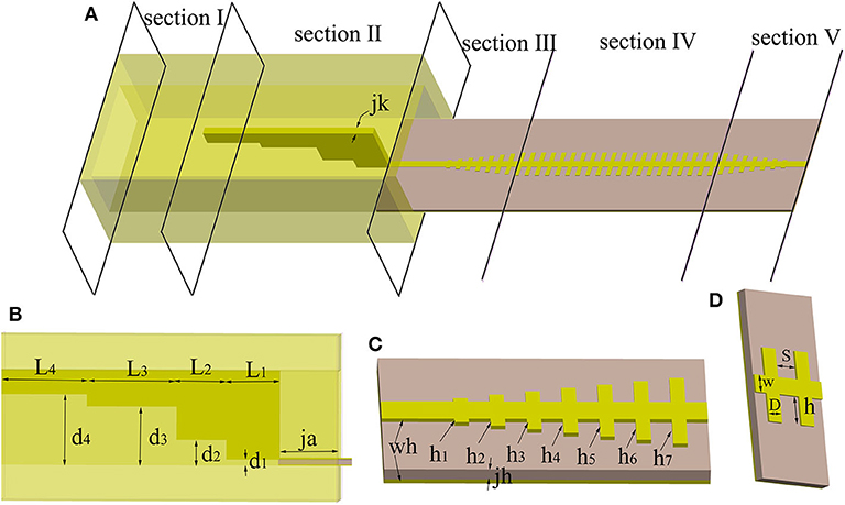
Figure 1. (A) The proposed conversion between the rectangular waveguide and the spoof SPPs TL. (B) Section II, the detail and geometric parameters of the stepped ridge. (C) Section III, the detail and geometric parameters of the seven gradient grooves. (D) Two unit cells in section IV.
Transition Between the Rectangular Waveguide and the Microstrip Line
Mode conversion and impedance matching between the rectangular waveguide and the microstrip line is achieved through stepped ridges, whose geometric features are depicted in Figure 2A. The principle of multi- quart-wavelength impedance transformation is applied, as sketched in Figure 2B. In this design, a four-step ladder ridge transition was adopted. By adjusting the length Li(i = 1, 2, 3, 4), height di(i = 1, 2, 3, 4), and the ridge thickness jk, one is able to flexibly adjust the impedance of the stepped ridge and achieve impedance matching at multiple operating frequencies, that is, to achieve a smooth and efficient transition between the waveguide and the microstrip line, and to widen the operating frequency band for broadband application.
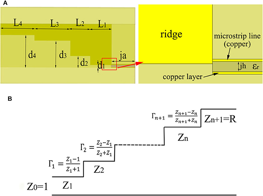
Figure 2. (A) Side-view of the stepped ridge (left) and the details at the junction between the ridge and the microstrip line (right). (B) Schematic diagram of the quarter-wavelength multi-section impedance converter.
Parameter study was carried out in the commercial software of CST so as to optimize the transition between the rectangular waveguide and the microstrip line in the entire Ku band. It was found that the reflection, which is represented by S11, is mainly determined by d1, L1and jk at the first ridge. Figure 3A indicates that in order to minimize the reflection in the entire working band, d1 should be neither too large nor too small. In other words, the bottom of the first ridge should be slightly lower than the top of the strip of the microstrip line. It is also observed in Figure 3B that the length of the first step ridge L1 has an optimal value around 4.6 mm. When L1 varies from the optimal value, the reflection increased accordingly. Figure 3C shows that the reflection and bandwidth is also sensitive to the thickness of the ridge jk. Finally, we optimized these three parameters together to make sure that S11 is lower than −15 dB and S21 is higher than −0.5 dB from 12.77 to 17.46 GHz, as is plotted in Figure 3D. It is noted that as the impedance matching is designed at the center frequency, the reflection and insertion loss increase slightly at the upper and lower side-bands.
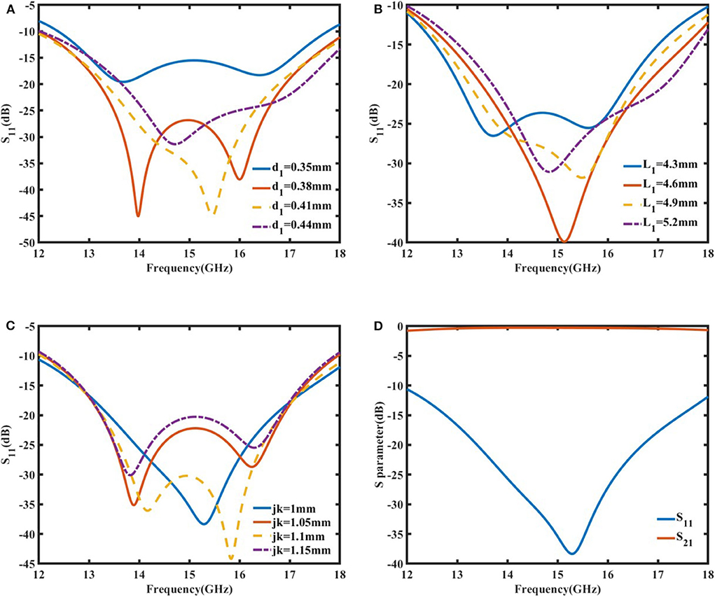
Figure 3. The simulated reflection (S11) when (A) the height d1, (B) the length L1, and (C) the thickness jk of the first ridge are changed. (D) The simulated reflection (S11) and transmission (S21) from the rectangular waveguide to the microstrip line when d1 = 0.42 mm, L1 = 4.8 mm, jk = 1 mm.
The above designed stepped ridge is demonstrated to effectively transfer the TE10 mode in the rectangular waveguide to the quasi-TEM mode in the microstrip line. Figure 4 demonstrates the mode conversion visually. In the rectangular waveguide, electric and magnetic field distributions of TE10 mode are observed clearly. On the right side of the stepped ridge, there is only negligible longitudinal component of electromagnetic field, indicating the quasi-TEM mode of the microstrip line.
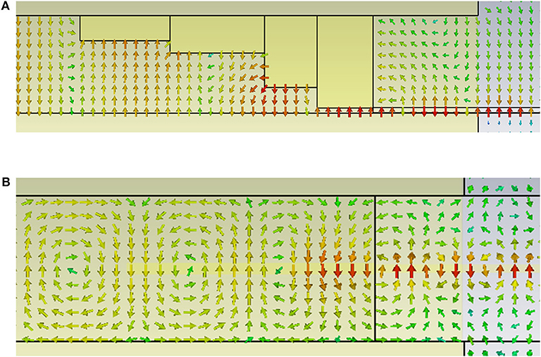
Figure 4. Mode conversion from the rectangular waveguide to the microstrip line with stepped ridge. (A) (side view) Distribution of the electric field. (B) (top view) Distribution of the magnetic field.
Transition Between the Microstrip Line and the Spoof SPP TL
Grounded metallic grooves are designed to support the propagation of spoof SPPs. By modifying geometric parameters in the unit (e.g., S, D, h in Figure 1D), one is able to design the dispersion curve of spoof SPPs. It has been investigated that as the operating frequency approaches the cut-off frequency, the attenuation of the spoof SPP TL increases accordingly [17]. Therefore, the dispersion curve is investigated in Eigen-mode simulation and the cut-off frequency is set to about 25 GHz so that the designed spoof SPP TL presents high transmission from 12 to 18 GHz.
For the purpose of impedance and momentum matching, transition section is needed between the microstrip line and the spoof SPP TL. It is noticed that the groove depth h has significant impact on the dispersion curve, as is plotted in Figure 5A, that as h increases the dispersion curve deviates quickly from the light line. In view of this, seven gradient grooves have been designed in the transition section with the groove depth hi = ih/8(i = 1, 2, ⋯ , 7) increasing evenly. The simulated S-parameters are shown in Figure 5B. In the entire Ku band, S11 is below −19 dB and S21 is above −1.2 dB. The insertion loss increases slightly as the frequency goes up toward the cut-off frequency, because the stronger field confinement results in more loss in metal and dielectric substrate. Overall, the transition between the microstrip line and the spoof SPP TL is smooth with high transmission and low return loss.
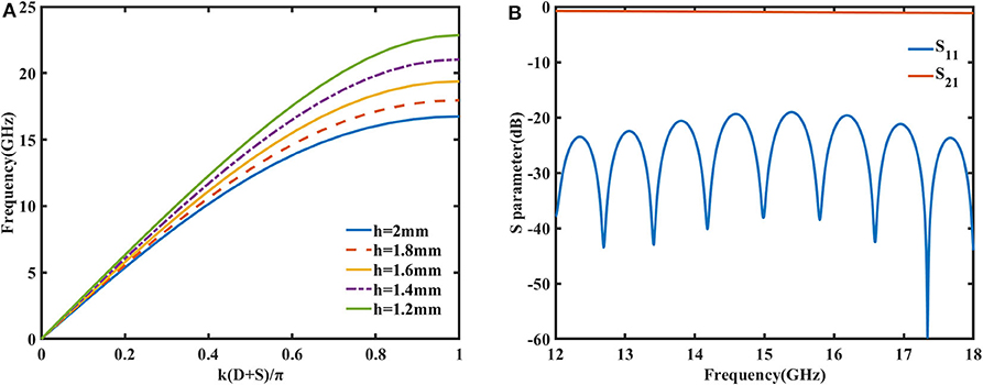
Figure 5. (A) The dispersion curves of the spoof SPPs when the depth of groove h varies. (B) The simulated S parameters from the microstrip line to the spoof SPP TL when seven gradient grooves are adopted as the transition section.
The proposed gradient grooves gradually transform the quasi-TEM wave in microstrip line to the TM mode spoof SPPs. Figure 6 gives the simulated electric and magnetic field distributions. Due to the existence of the grooves, the electric field gradually appears to have the longitudinal component, as is observed in Figure 6A. In contrast, the magnetic field in Figure 6B is always in the transverse plane, which guarantees the transverse magnetic mode of spoof SPPs.
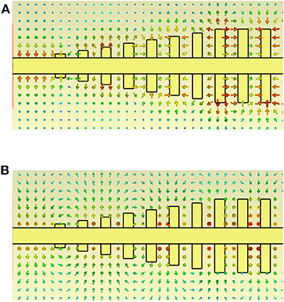
Figure 6. Mode conversion from the microstrip line to the spoof SPP TL (top view). (A) Distribution of the electric field. (B) Distribution of the magnetic field.
Fabrication and Experiment
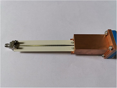
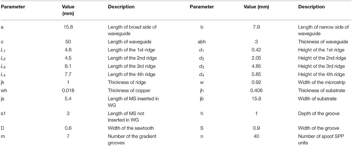
A prototype of the design is fabricated and measured for demonstration. A WR-62 standard rectangular waveguide with stepped ridges is manufactured using copper and assembled from three separately machined parts. The microstrip line and the spoof SPP TL are printed on the substrate of Rogers RO4003C with a thickness of 0.406 mm and the relative permittivity of 3.55. The ground of the TLs is seated on the bottom inner wall of the rectangular waveguide using two plastic screws, as is shown in Figure 7, so as to stably locate and assemble the TLs and the rectangular waveguide. Detailed parameters after optimization are listed in Table 1 for the readers' information.
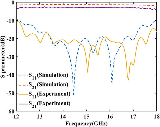
In measurement, the rectangular waveguide is connected to Port One of an Agilent Vector Network Analyzer (VNA) through a coaxial cable and a flange. At the output (on the right side in Figure 7), the microstrip line is connected to an SMA connector and then to Port Two of the VNA. The Scattering parameters are measured and plotted in Figure 8. It is observed that the measured reflection (S11) is always below −10 dB from 12 to 18 GHz, and below −15 dB from 12.3 to 17.75 GHz. The measured S11 curve is similar to the simulated one except for a slight shift to the higher frequency. Considering that the reflection is sensitive to some geometric parameters, e.g., d1 and jk as shown in Figure 3, the slight difference between the simulated and measured results is mainly because of the inaccuracy during machining of the waveguide and assembling of the samples. On the other hand, the measured transmission coefficient (S21) is above −3.5 dB from 12 to 17.9 GHz, and above −3 dB from 12.3 to 17.2 GHz. It has been discussed above that in simulation the insertion loss comprises the losses in the two-step transition. In measurement, the S21 curve is as flat as the simulated one, although with a further reduction of about 1.5 dB. This further reduction may be due to the fabrication and assembling error of the prototype, or the loss of metal and substrate at Ku band. Nevertheless, the measured results have proved the broadband and high-efficiency excitation of spoof SPPs through the rectangular waveguide.
Discussion and Conclusion
In this work, we proposed a method to excite spoof SPPs through conventional rectangular waveguide with high efficiency and wideband performance. This is a two-step procedure with the first transition from the rectangular waveguide to the microstrip line and the second from the microstrip line to the spoof SPP TL. A prototype was designed, fabricated and measured from 12 to 18 GHz for demonstration. Good transmission and low reflection are observed in both simulation and measurement. The proposed scheme can be extended for non-grounded spoof SPP TLs with different transitions from the microstrip line [18]. This method may have great potentials to provide an easy and low-cost way to feed plasmonic circuits at microwave, millimeter wave and Terahertz.
Data Availability Statement
All datasets presented in this study are included in the article/supplementary material.
Author Contributions
WT and TC conceived the idea, suggested the designs, and supervised the work. WT and JW conducted the analytical modeling and wrote the manuscript. JW, XY, and JL conducted the numerical simulations and modifications. WT, XG, and LZ conducted sample assembly and measurements. All authors contributed to the article and approved the submitted version.
Funding
This work was supported in part from the National Science Foundation of China under Grant nos. 61631007 and 61971134, in part from the 111 Project under Grant no. 111-2-05, and in part from the Fundamental Research Funds for the Central Universities under Grant no. 2242020R40079.
Conflict of Interest
The authors declare that the research was conducted in the absence of any commercial or financial relationships that could be construed as a potential conflict of interest.
References
1. Raether H. Surface Plasmons on Smooth and Rough Surfaces and on Gratings. Berlin; Heidelberg: Springer (1988). doi: 10.1007/BFb0048317
2. Maier SA. Plasmonics: Fundamentals and Applications. New York, NY: Springer (2007). doi: 10.1007/0-387-37825-1
3. Pendry J, Martin-Moreno L, Garcia-Vidal F. Mimicking surface plasmons with structured surfaces. Science. (2004) 305:847–8. doi: 10.1126/science.1098999
4. Hibbins AP, Evans BR, Sambles JR. Experimental verification of designer surface plasmons. Science. (2005) 308:670–2. doi: 10.1126/science.1109043
5. Maier SA, Andrews SR, Martin-Moreno L, Garcia-Vidal FJ. Terahertz surface plasmon-polariton propagation and focusing on periodically corrugated metal wires. Phys Rev Lett. (2006) 97:176805. doi: 10.1103/PhysRevLett.97.176805
6. Garcia-Vidal FJ, Martin-Moreno L, Pendry JB. Surfaces with holes in them: new plasmonic metamaterials. J Opt A Pure Appl Opt. (2005) 7:S97–101. doi: 10.1088/1464-4258/7/2/013
7. Shen X, Cui TJ, Martin-Cano D, Garcia-Vidal FJ. Conformal surface plasmons propagating on ultrathin and flexible films. Proc Nat Acad Sci USA. (2013) 110:40–5. doi: 10.1073/pnas.1210417110
8. Liu X, Feng Y, Zhu B, Zhao J, Jiang T. High-order modes of spoof surface plasmonic wave transmission on thin metal film structure. Opt Express. (2013) 21:3155–65. doi: 10.1364/OE.21.031155
9. Wu JJ, Hou DJ, Liu K, Shen L, Tsai CA, Wu CJ, et al. Differential microstrip lines with reduced crosstalk and common mode effect based on spoof surface plasmon polaritons. Opt Express. (2014) 22:26777–87. doi: 10.1364/OE.22.026777
10. Liang Y, Yu H, Zhang H, Chang Y, Cui TJ. On-chip sub-terahertz surface plasmon polariton transmission lines in CMOS. Sci Rep. (2015) 5:14853. doi: 10.1038/srep14853
11. Ma HF, Shen X, Cheng Q, Jiang WX, Cui TJ. Broadband and high-efficiency conversion from guided waves to spoof surface plasmon polaritons. Laser Photonics Rev. (2014) 8:146–51. doi: 10.1002/lpor.201300118
12. Zhang WJ, Zhu GQ, Sun LG, Lin FJ. Trapping of surface plasmon wave through gradient corrugated strip with underlayer ground and manipulating its propagation. Appl Phys Lett. (2015) 106:021104. doi: 10.1063/1.4905675
13. Zhang Q, Zhang HC, Wu H, Cui TJ. A hybrid circuit for spoof surface plasmons and spatial waveguide modes to reach controllable band-pass filters. Sci Rep. (2015) 5:16531. doi: 10.1038/srep16531
14. Liu LL, Li Z, Xu BZ, Gu CQ, Chen C, Ning PP. High-efficiency transition between rectangular waveguide and domino plasmonic waveguide. AIP Adv. (2015) 5:027105. doi: 10.1063/1.4907879
15. Liu LL, Li Z, Gu CQ, Chen C, Ning PP, Xu BZ, et al. Smooth bridge between guided waves and spoof surface plasmon polaritons. Opt Lett. (2015) 40:1810–3. doi: 10.1364/OL.40.001810
16. Liu LL, Li Z, Xu BZ, Gu CQ, Xu J, Chen C, et al. Ultra low loss high-contrast gratings based spoof surface plasmonic waveguide. IEEE Trans Microw Theory Tech. (2017) 65:2008–18. doi: 10.1109/TMTT.2017.2662235
17. Zhang HC, Zhang Q, Liu JF, Tang WX, Fan YF, Cui TJ. Smaller-loss planar SPP transmission line than conventional microstrip in microwave frequencies. Sci Rep. (2016) 6:23396. doi: 10.1038/srep23396
Keywords: spoof surface plasmon polaritons, microwave, rectangular waveguide, excitation, mode transition
Citation: Tang W, Wang J, Yan X, Liu J, Gao X, Zhang L and Cui TJ (2020) Broadband and High-Efficiency Excitation of Spoof Surface Plasmon Polaritons Through Rectangular Waveguide. Front. Phys. 8:582692. doi: 10.3389/fphy.2020.582692
Received: 13 July 2020; Accepted: 21 August 2020;
Published: 30 September 2020.
Edited by:
Fei Gao, Zhejiang University, ChinaReviewed by:
Zhuo Li, Nanjing University of Aeronautics and Astronautics, ChinaKuang Zhang, Harbin Institute of Technology, China
Copyright © 2020 Tang, Wang, Yan, Liu, Gao, Zhang and Cui. This is an open-access article distributed under the terms of the Creative Commons Attribution License (CC BY). The use, distribution or reproduction in other forums is permitted, provided the original author(s) and the copyright owner(s) are credited and that the original publication in this journal is cited, in accordance with accepted academic practice. No use, distribution or reproduction is permitted which does not comply with these terms.
*Correspondence: Wenxuan Tang, d2VueHVhbnQmI3gwMDA0MDtzZXUuZWR1LmNu; Tie Jun Cui, dGpjdWkmI3gwMDA0MDtzZXUuZWR1LmNu
†These authors have contributed equally to this work
 Wenxuan Tang
 Jiangpeng Wang
 Xiaotian Yan
 Junfeng Liu
 Xinxin Gao
 Lepeng Zhang
 Tie Jun Cui