- 1Key Laboratory of Electromagnetic Wave Information Technology and Metrology of Zhejiang Province, College of Information Engineering, China Jiliang University, Hangzhou, China
- 2Centre for THz Research, China Jiliang University, Hangzhou, China
- 3State Key Laboratory of Crystal Materials, Shandong University, Jinan, China
A tunable graphene terahertz metamaterial absorber is designed by treating a monolayer continuous dumbbell-shaped structure graphene layer, which can simultaneously realize the narrow bandwidth and dual-band absorption with transverse magnetic (TM) polarization and wide incident angle operation. Two pronounced absorption peaks are caused by the novel toroidal dipole phenomenon and magnetic plasmon polariton. By optimizing the geometry parameters, the relative narrow bandwidths of the two absorption peaks are 26.4 and 23.5 GHz at frequencies of 0.2242 THz and 0.5302 THz, respectively, with the absorption rate above 99.6%. Since the continuous dumbbell-shaped graphene structure is treated in the absorber, a more convenient way to realize the tuning ability by treating a bias voltage compared to the absorbers with discrete graphene structures. The designed device can work at a wide incident angles (up to 80°) under TM polarization with the absorption above 88% at low frequency. The simulation results are basically in good agreement with the results of the equivalent circuit model. This work offers huge potential applications in terahertz imaging, detecting and sensing, especially in the 6G communication systems.
Introduction
The standardization of fifth generation (5G) communications has been finished, and the 5G network will be built into commercial applications in 2020. Based on the above fact, the outlook and development plan of 6G communications has been put on the agenda, laying a foundation for the new generation of communication systems for future needs of the 2030s [1]. The terahertz band ranged from 0.1 to 10 THz is referred to as a gap region located between the microwave and optical spectra. Because of its huge application potential in communication, biomedical imaging, security, and so on, terahertz technology has caught increasing attention in recent years.
The pivotal problem influencing the actual application in hybrid terahertz/free-space-optical systems expected to be implemented in 6G frequency band is the shortage of functional devices with outstanding characteristics. This is mainly caused by the shortage of the materials in nature that can directly interact with terahertz waves. To overcome this problem, an artificial composite material containing periodically arranged structural units named metamaterial is proposed and investigated. Different from nature materials, by designing the resonant unit structure, the metamaterial can provide some abnormal electromagnetic characteristics, including negative refractive index [2], invisibility [3], perfect absorption [4] and electromagnetic induced transparency [5]. Based on their unique electromagnetic characteristics, metamaterial has been applied in terahertz function devices, including sensors [6, 7], modulators [8], filters [9], and switches [10].
Metamaterial absorbers showcase huge application value in communication, security, detection and other fields, and have increasingly become one of the study hotspots in terahertz region [11–20]. Landy et al. reported a metamaterial absorber with perfect absorption characteristics for the first time [21]. Since then, various metamaterial absorbers operating in various frequency regions were achieved, from microwave to infrared range [22–24]. In terahertz region, Tao et al. demonstrated the first narrowband absorber [25]. Therefore, dual-band and multi-band terahertz absorbers were put forward continuously. For the proposed absorbers, the characteristics have been realized on the basis of the geometry structures, which restrict their practical applications. There is an urgent need to actively modulate and control the metamaterial absorbers by applying heat, electric field, magnetic field and optical field.
In recent years, researchers have treated some functional material to design tunable terahertz metamaterial absorbers. Yin et al. showed a terahertz tunable dual-band metamaterial absorber by employing the liquid crystal material [26]. Liu et al. proposed a thermally tunable broadband terahertz metamaterial absorber on the basis of the mixed VO2 [27]. Caused by the excellent transition characteristics of VO2 material, the maximum tuning range of the designed device can be changed from 5 to 100% by treating an external thermal field. Zhang et al. designed a tunable metamaterial terahertz absorber treating 3D Dirac semimetal films (DSF) [28]. The operating characteristics of the DSF absorber can be dynamically tuned by changing the Fermi level instead of structure geometry parameters. Recently, they also reported a tunable broadband metamaterial sandwich-structured terahertz absorber containing black phosphorous and vanadium dioxide [29]. The dynamical tuning operation of the broadband absorption is resulted from the variation of the electron doping of black phosphorous and conductivity of VO2. Huang et al. designed a metamaterial absorber based on temperature variation that contains a periodic array of metal circle resonators with strontium titanate [30]. Gu et al. designed and fabricated a new kind of Salisbury screen absorber formed by DAST crystalline films [31]. The terahertz response of the absorber can be adjusted by changing the thickness of the DAST film and the spacer. On the other hand, graphene-assisted switchable liquid crystal terahertz metamaterial absorber was reported by Wang et al. [32]. However, the limitation of the tuning range of the material constitutive parameters will restrict the realization of the narrow band absorption performance.
How to obtain tunable narrow-bandwidth dual-band absorption is a hot research topic in graphene-based metamaterial absorber. One way to realize the multiband absorbers is to use multi-resonator structures in one unit cell [33, 34]. Another way is to superimpose the multi-layered graphene structures with different geometric sizes [35]. Although the characteristics of the tunable dual-band absorption are ideal, however, the bandwidths of the absorption peaks are wide and cannot satisfy the narrow-bandwidth requirements in 6G or terahertz communication systems. It is a very difficult task to combine the two properties of dual-band and narrow bandwidth with simple manufacturing process.
Motivated by the previous studies, in this work, a dual-band tunable metamaterial absorber with narrow bandwidth in the terahertz region is designed by using a simple sandwich structure. The absorber is formed by a dumbbell-shaped monolayer graphene metasurface layer and a gold ground plane, and the two layers are separated by a silicon layer. The theoretical and numerical investigation on the internal mechanism of narrow-bandwidth dual-band tunable absorber are performed based on CST Microwave Studio and equivalent circuit model. The absorption characteristics of the designed metamaterial absorber are analyzed by optimizing different parameters of graphene geometry, substrate thickness, and incident angle of terahertz wave. The results demonstrate that the absorption can reach 99.62 and 99.76% at 0.2242 and 0.5302 THz with the extreme narrow bandwidths as low as 26.4 and 23.5 GHz, respectively. The designed absorber offers dual-band absorption, high absorptivity, polarization-sensitivity and wide incident angles. In addition, the tenability of the terahertz absorptivity and the absorption peaks can be achieved conveniently by changing the bias voltages.
Structural Design and Research Techniques
The unit cell of the dumbbell-shaped graphene structure metamaterial absorber is depicted in Figure 1. The metamaterial structure used in this paper is formed by a planar array of continuous graphene structure suspended in a rectangular dielectric silicon layer and a metal ground plane. The structure of the graphene layer is a dumbbell shape and aligned with y-axis (see Figure 1). The detailed geometric parameters are defined in the caption of Figure 1A. As shown in Figure 1B, the graphical graphene periodic array is fabricated on top of silicon layer. The voltage V between the gold plate and the metal electrode is used to change the chemical potential of graphene. The excitation signal is a linear polarized plane wave with transverse magnetic (TM) polarization transmitting along the z direction. At resonance, the normal incident plane wave radiation, polarized along x-axis, will cause dipole effects along x-axis, as depicted in Figure 1. These excitations will couple with the free-space radiation and result in the absorption characteristics of the metamaterial structure [36]. The dielectric material used in this paper is lossless silicon with relative permittivity εr = 11.9 [37, 38]. Gold is treated as the ground plane with conductivity σgold = 4.561 × 10⁷ S/m [38]. The thickness of the graphene layer can be set as h_g = 1 nm. Other parameters are listed as follow: r = 55 μm, d = 95 μm, dx = 35 μm, h_m = 50 μm, t = 0.2 μm, Px = 200 μm and Py = 450 μm.
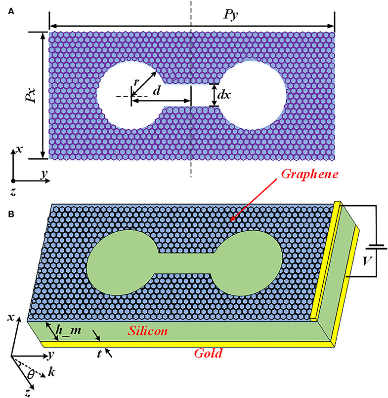
Figure 1. (A) Structure of the dumbbell-shaped graphene layer; (B) Schematic of the designed terahertz perfect absorber, including a top layer of continuous graphene metasurface, a middle layer of the silicon dielectric layer, and a metal gold plate. Geometry parameters here: Px = 200 μm, Py = 450 μm, r = 55 μm, d = 95 μm, dx = 35 μm, h_m = 50 μm, and t = 0.2 μm.
The permittivity of the graphene can be expressed as [39]:
where ω defines the terahertz frequency, tg represents the thickness of the graphene layer, ε0 denotes the permittivity of vacuum. Surface conductivity of graphene σ(ω) = σintra(ω) + σinter(ω) can be obtained on the basis of the Kubo formula [5], containing the interband and intraband transition contributions. In terahertz frequencies, the interband transitions can be neglected caused by the Paili Exclusion Principle, and at room temperature (T = 300 K), the Kubo formula can be expressed by a Drude-like expression [40, 41]:
where e is the electron charge, and ℏ represents the reduced Planck constant. μc denotes the chemical potential. The carrier relaxation time τ = μμc/(ev2 f) [42], where vf denotes the Fermi velocity (the value is 106 m/s here). μ represents the carrier mobility., which relies mainly on the fabrication method. Higher carrier mobility higher than 10,000 cm2/(Vs) was achieved for graphene grown by chemical vapor deposition (CVD) [43]. Also, the mobility in excess of 200,000 cm2/(Vs) was obtained experimentally based on suspended monolayer graphene [44]. In view of the feasibility of practical applications, an appropriate mobility of 10,000 cm2/(Vs) could be assumed in our design. Recently, by fabricating the graphene layer on hexagonal Boron nitride (h-BN) substrate, the high mobility of 50,000 cm2/(Vs) was realized at room temperature based on CVD method, and the carrier mobility increased to 300,000 cm2/(Vs) at ultralow temperature [45]. h-BN has no dangling bonds and its atomic structure is flat. Also, h-BN can provide a much less amount of charge traps than silicon dioxide [46]. In addition, it shows a minor lattice mismatch with graphene. Thus, a monolayer graphene manufactured on h-BN demonstrates the tendency to provide a much higher mobility.
Numerical simulations are investigated based on the commercial software CST Microwave Studio [47]. The frequency domain solver is treated in simulation to calculate the reflection coefficient |S11| and the transmission coefficient |S21|. Open boundary condition is set in the z direction and unit cell boundary conditions are used in the x and y directions. Adaptive tetrahedral mesh refinement is adopted to improve the simulation accuracy. The absorption of the metamaterial structure can be calculated by the expression A = 1–|S21|2–|S11|2, where the transmission |S21|2 can be neglected since the gold plate prevents the terahertz wave from going through the absorber. In the simulation, the electric field of terahertz wave paralleled to the x axis is defined the TM polarization while the electric field paralleled to the y axis is TE polarization.
Results and Discussion
The absorption characteristics of the designed dumbbell-shaped dual-band metamaterial absorber at normal incidence for TM polarization illustrate in Figure 2A. The red and black curves indicate the absorption and reflection of the TM polarization, respectively. Because the continuous gold plate is placed on the bottom of the absorber, the transmittance of the absorber is zero. The blue line denotes the absorption of TE polarization. For the two absorption peaks of TM polarization, the maximum absorptions are 99.62 and 99.76% at frequencies of 0.2242 and 0.5302 THz with the excellent narrow bandwidths as low as 26.4 and 23.5 GHz, respectively. The color map shown in Figure 2B reveals the relationship between the absorption and the terahertz frequency with different polarization angles φ changing from 0° to 90° with a step of 5°. The characteristic of the two absorption peaks is changed over the interested frequency as the polarization angle φ changing. This result reveals the polarization-dependent characteristic of the absorption at normal incidence.
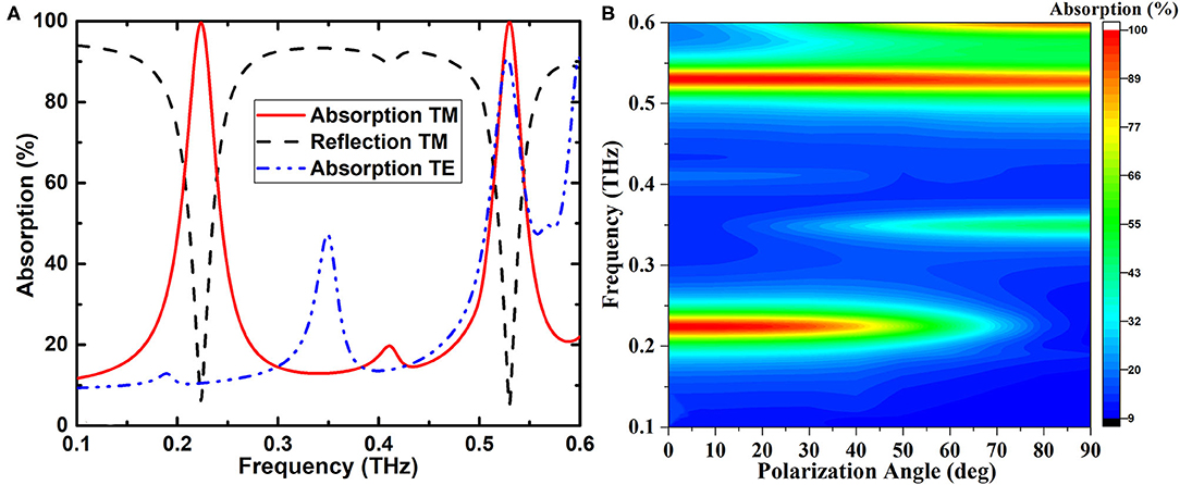
Figure 2. (A) Absorption and reflection of the dual-band absorber. (B) Relationship between the absorption and the terahertz frequency with different polarization angles φ changing from 0° to 90°.
In order to furtherly figure out the physical origin of dual-band absorption characteristic, the electric field at absorption peaks of 0.2242 THz and 0.5302 THz with TM- and TE-polarizations are given in Figure 3. The physical mechanism of the dual-band perfect absorber designed in this paper has relation to the electric dipole resonance in dumbbell-shaped structure array, which is attributed to the local surface plasmon resonance and magnetic dipolar resonance between the graphene microstructure and the gold plate [34]. For TM polarization, as depicted in Figures 3A,B, the physical mechanism of the two absorption peaks is different. In Figure 3A, when the resonant frequency is 0.5302 THz, the induced electric fields concentrate mostly around the edges of the graphene dumbbell-shaped metasurfaces. In this case, charges with opposite polarity will store up at the left and right halves of each graphene microstructure along the x direction, resulting in the capacitive properties [38]. The surface current distributions of the absorber at the resonant frequencies are also given in Figure 4 to explain the resonance type. At the resonant frequency of 0.5302 THz (given in Figure 4A), the direction of surface currents of the dumbbell-shaped graphene layer is opposite to the surface currents direction of the gold ground plane. The resonance type at absorption peak of 0.5302 THz can be deemed to the magnetic plasmon excitation. When the frequency is 0.2242 THz, as depicted in Figure 3B, the excited electric fields mainly concentrate at the edges of the middle part of the dumbbell-shaped graphene layer. As depicted in Figure 4B, when the resonant frequency is 0.2242 THz for TM polarization, the opposite circular displacement currents surround the two ends of the dumbbell-shaped structure simultaneously. Two magnetic fields with different directions along the z direction will be excited by the two ring currents. The excited magnetic fields show low radiation characteristics and will generate a circular magnetic moment perpendicular to the graphene layer. Thus, the head-to-tail connection magnetic moment results in the toroidal dipole moment in the x direction [36, 48]. With the above discussion, the absorption peak at the resonant frequency of 0.2242 THz is caused by the toroidal dipole phenomenon in the dumbbell-shaped graphene layer. The detail investigation about the toroidal dipole will be reported in our future work. For the terahertz wave with TE polarization, since no resonant mode is excited at the frequency around 0.2 THz, there is no absorption peak appears around 0.2 THz in the absorption spectrum shown in Figure 2.
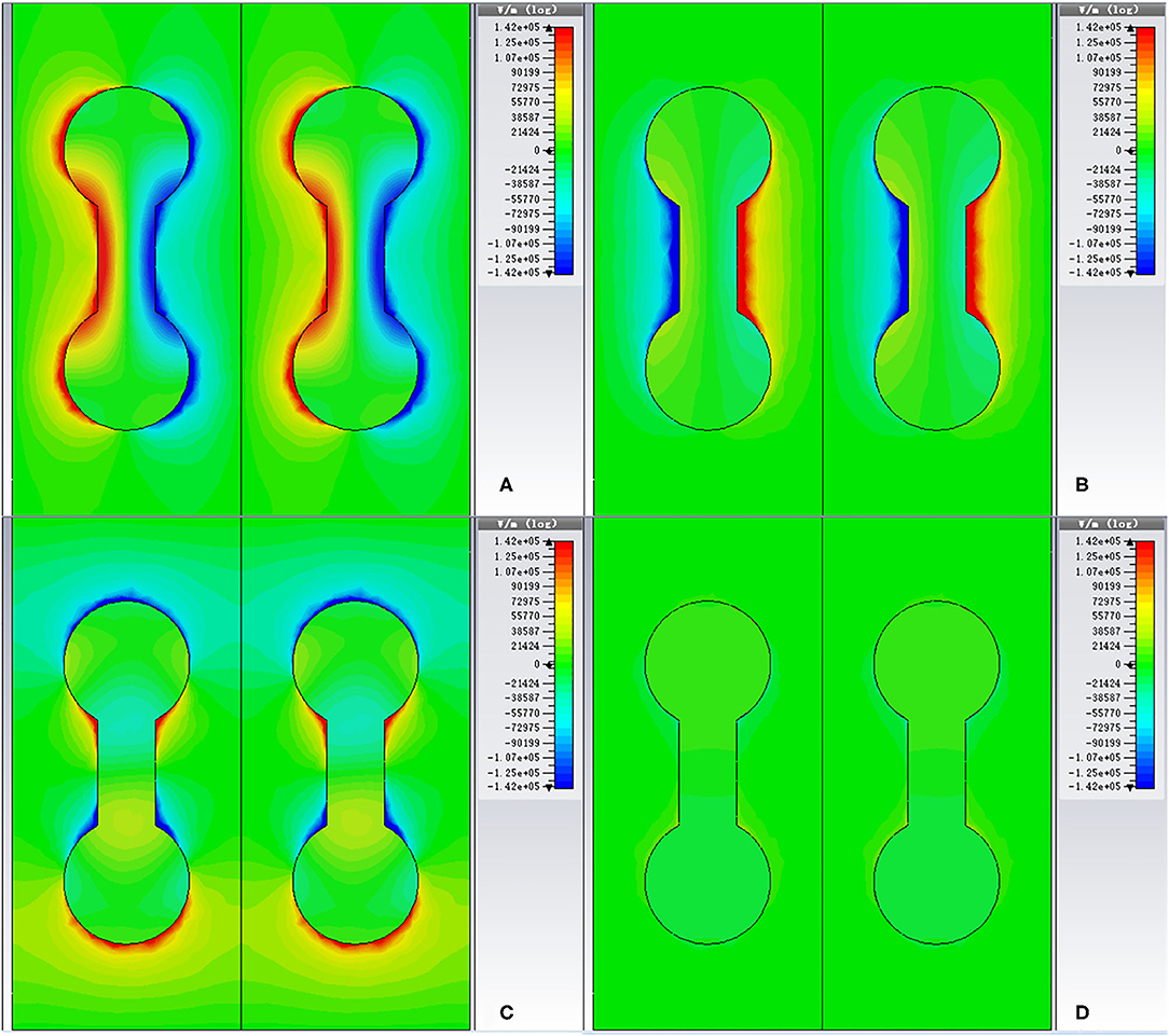
Figure 3. Induced electric field distributions of the dumbbell-shaped graphene absorber for different modes: (A) TM for 0.5302 THz; (B) TM for 0.2242 THz; (C) TE for 0.5302 THz; (D) TE for 0.2242 THz.
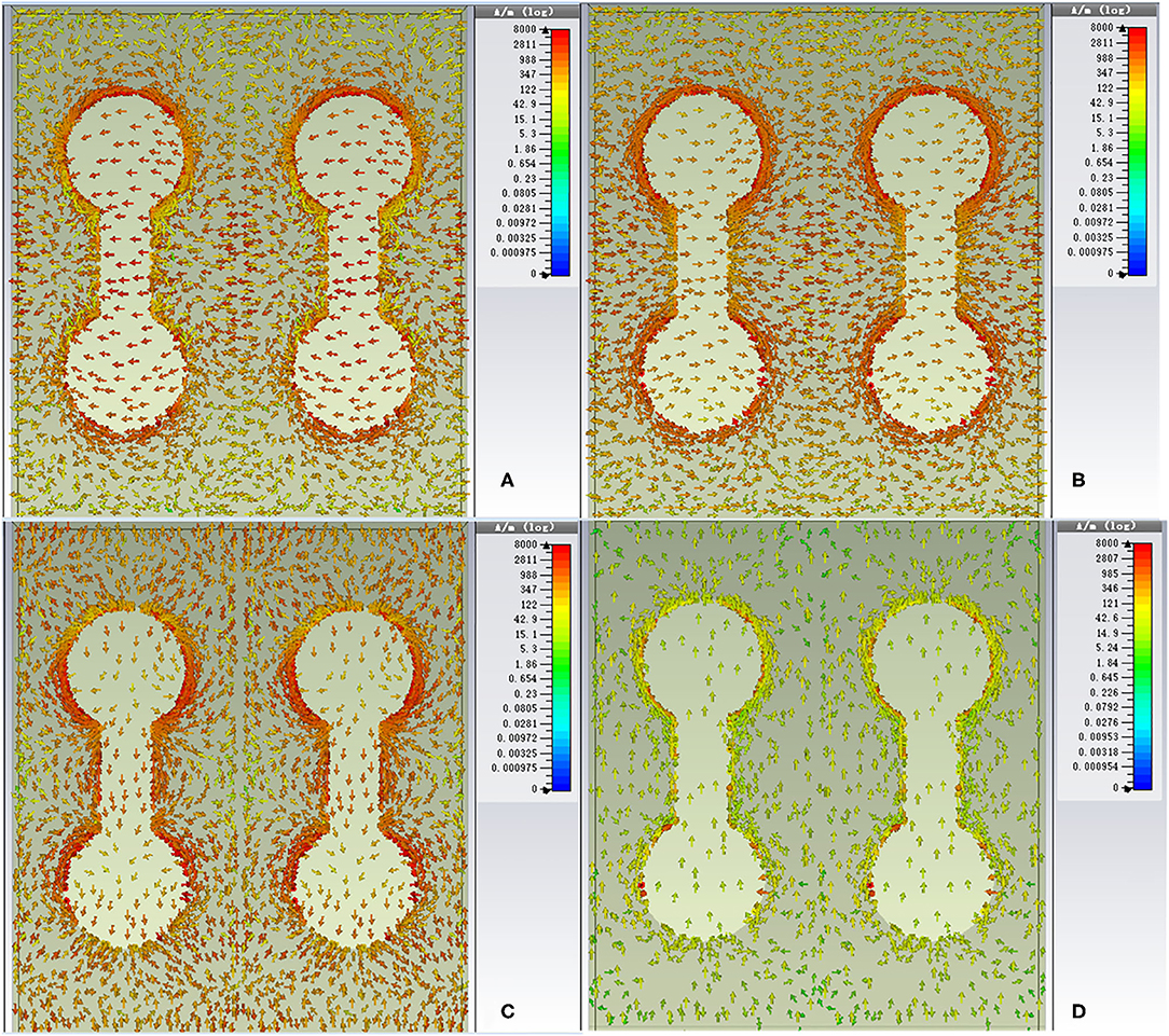
Figure 4. Induced surface current distributions of the dumbbell-shaped graphene absorber for different modes: (A) TM for 0.5302 THz; (B) TM for 0.2242 THz; (C) TE for 0.5302 THz; (D) TE for 0.2242 THz.
The impact of various geometry parameters of the absorber on the absorption performances are investigated. The absorption spectra of the designed dumbbell-shaped narrow bandwidth metamaterial absorber with different silicon substrate thickness h_m, distance d, width dx and radius r in frequency band of 0.1–0.6 THz, are shown in Figure 5. Figure 5A demonstrates that the thickness variation of the silicon layer will slightly influence the absorption rate and the shift of the resonant peak simultaneously. When the thickness of the silicon layer (h_m) increases from 45 to 60 μm, the two absorption peaks depicts red-shift. Also, the absorption around peak frequency of 0.22 THz increases gradually and the absorption around peak of 0.53 THz increases first and then decreases. As given in Figure 5B, the change of the distance d between the two circles demonstrates a slight impact on the absorption rete and shift of the two absorption peaks. When d increases from 85 to 105 μm, the two absorption peaks exhibit red-shift. However, the absorption peak around 0.53 THz with d = 100 μm doesn't satisfy the red-shift rule. Figure 5C depicts that as the width dx increasing from 25 to 50 μm, the resonant peak around 0.22 THz shows blue-shift, while the resonant peak around 0.53 THz is almost unchanged. As depicted in Figure 5D, when the radius r of the circles changes, the two absorption peaks are almost unchanged. Based on the above parameters analysis, the optimal geometrical parameters are concluded as follows: d = 95 μm, dx = 35 μm, r = 55 μm and h_m = 50 μm.
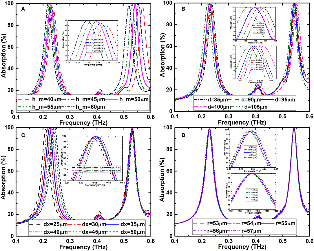
Figure 5. Absorption spectra under (A) different dielectric layer thickness h_m when d = 95 μm, dx = 35 μm, r = 55 μm; (B) different distance d when h_m = 50 μm, dx = 35 μm, r = 55 μm; (C) different width dx when h_m = 50 μm, d = 95 μm, r = 55 μm; (D) different radius r when h_m = 50 μm, d = 95 μm, dx = 35 μm.
The influence of carrier mobility μ of graphene on the operation performance of the designed dual-band metamaterial absorber is demonstrated. Based on the discussion given in section Methods, when the chemical potential is fixed at μc = 1 eV, the absorption spectra of the absorber with different values of μ changing from 1,000 cm2/(Vs) to 50,000 cm2/(Vs)are discussed and given in Figure 6. The change of μ doesn't affect the location of the absorption peak. When the carrier mobility μ is higher, the absorption decreases caused by the higher loss. On the contrary, the absorption peaks become more non-significant with the increase of μ, and the absorption of the two absorption peaks decreases.
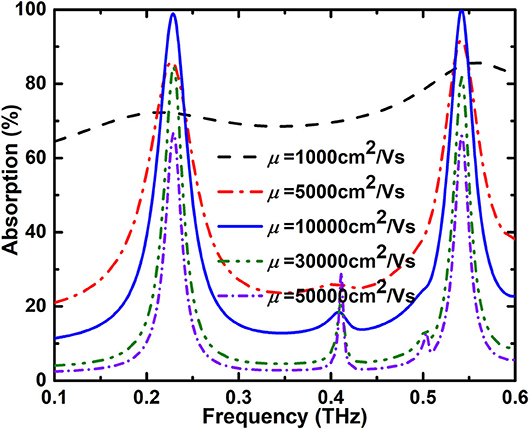
Figure 6. Absorption spectra of the dual-band absorber with different values of μ from 1,000 to 50,000 cm2/(Vs) with μc = 1 eV.
For the graphene-based terahertz devices, one of the major merits is the dynamic tenability that the traditional devices cannot provide. The optical characteristics of the designed graphene absorber can be manipulated by changing the chemical potential μc of graphene instead of reconstructing the physical structure. In this paper, the electric tuning can be obtained by applying a bias voltage since the dumbbell-shaped graphene structure of the design absorber is continuous. The continuous graphene structure has the advantage of being easy to manufacture. The variation of the graphene chemical potential can be realized based on the adjustment of the voltage between the electrode and the ground plane. Figure 7 depicts the absorption spectra of the dual-band absorber with different μc from 1.6 to 0.2 eV. When μc = 1.6 eV, the two resonant peaks locate at 0.2296 and 0.5419 THz with the absorption of 89.17 and 94.05%, respectively. And the corresponding narrow bandwidths are 27.87 and 24.82 GHz, respectively. When the chemical potential μc decreases from 1.6 to 0.2 eV, the two absorption peaks slightly red shifted. Meanwhile, the spectral bandwidth of the two absorption peaks become smaller first and then become larger. When the chemical potential is μc = 1 eV, the absorption of the two peaks of 0.2242 THz and 0.5302 THz are 99.62 and 99.76% with the bandwidth of 26.4 and 23.5 GHz, respectively. When the chemical potential furtherly decreases, the absorption peaks disappeared, and only a wide absorption band with the absorption above 91% in the interested frequency range is achieved. Here, the excited absorption peaks realize a maximum absorption change from 99.62 to 73.40% around 0.2 THz and 99.76 to 80.56% around 0.5 THz, which located in the 6G-communication frequency band.
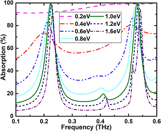
Figure 7. Relationship between the absorptivity and frequency with different chemical potentials from 0.2 to 1.6 eV.
The performance of the designed absorber under arbitrary incidence with TM polarization is investigated and illustrated in Figure 8. Figure 8 shows that the frequency of the lower absorption peak slightly increases with the increase of the incident angle of TM polarization, resulting in the absorption peak being divided into two. This phenomenon may be caused by the parasitic resonances in the structure at a large incident angle [49]. Meanwhile, the higher absorption peak moves to high frequencies. This result can be explained that the variation of the electrical length will influence the magnetic resonance frequency. However, the absorption of the lower frequency absorption peak can still keep above 88% under 80° incidence.
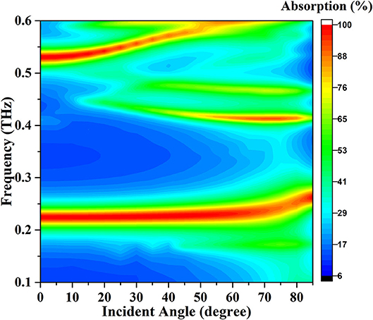
Figure 8. Absorption spectra for the designed perfect absorber with different frequencies and incident angles for TM polarization.
In order to prove the superiority of the designed absorber, result comparison with reported terahertz graphene absorbers is listed in Table 1. The results illustrate that the dual-band absorber designed here can provide the excellent narrow absorbing bandwidths with two tunable absorption peaks, which can be widely used in the 6G-communication systems. Furthermore, since only one monolayer continuous graphene layer is treated in the design, the metamaterial absorber is easy to fabricate and tune.
RLC Circuit Model
The equivalent circuit model can be used to qualitatively forecast the behavior of the structures and the characteristics of the designed absorber. Furthermore, the impact of the geometry and periodic structure on the performance of absorber can also be estimated. Thus, the equivalent circuit model is beneficial for designing the new applications and providing physical mechanism of absorbers.
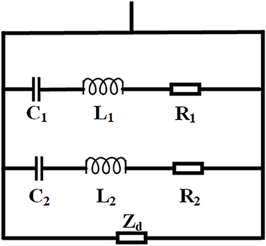
Based on the equivalent circuit model, the dual-band metamaterial absorber can be equivalently modeled as an equivalent circuit containing parallel-connected two series RLC circuits illustrated in Figure 9. Hence, the interaction between the terahertz wave and the absorbers can be investigated based on the transmission line theory.
By investigating the numerical simulation results, the value of the reflection coefficient S11 corresponding to the resonance point can be used to approximate the lumped parameter values of R, L, and C in the equivalent circuit [54–56].
ZR is the surface impedance of microstructure which can be expressed as:
The value R can be obtained by:
By taking two points ω1 and ω2 near the low-frequency resonant peak around 0.2 THz, the values of the capacitor C1 and inductor L1 in the equivalent circuit can be obtained by:
Similarly, by taking two points ω3 and ω4 near the high-frequency resonant peak around 0.53 THz, the values of the capacitor C2 and the inductor L2 in the equivalent circuit can be achieved.
The silicon layer and gold ground plane can be regarded as a shot-circuited transmission line with the length of d, and the impedance can be expressed as:
where , c represents the wave speed in vacuum, θ defines the angle of incidence terahertz wave. is the intrinsic impedance with TM polarization, is the intrinsic impedance with TE polarization.
Zd can be equivalent by the series connection of inductor Ld and capacitor Cd. The Cd and Ld can be calculated by using two frequency points ω5 and ω6 around the high-resonant frequency:
Table 2 summarizes the parameters of the equivalent circuit calculated by optimizing the RLC parameters based on the above equations.
Figure 10 illustrates the absorption of the absorber based on the calculation from equivalent circuit model and full wave simulation, respectively. The results obtained from equivalent circuit agree well with the full-wave simulation results.
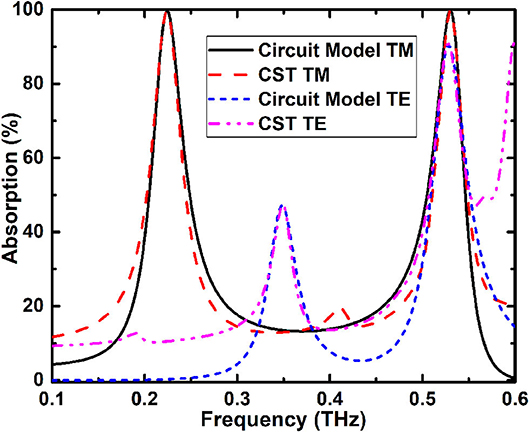
Figure 10. Comparison of simulation results and equivalent circuit calculated results of the tunable dual-band absorber with TE and TM polarizations.
Finally, the working speed of the designed absorber depends on the RC value, where the capacitor C is mainly caused by the stray capacitance between the graphene layer and the dielectric substratum [40]. The capacitance can be expressed as C = ε0εdSg/d, where ε0 represents the permittivity of vacuum, εd represents the relative permittivity of silicon, d = 55 μm defines the thickness of silicon, and Sg is the total effective area of graphene. In this work, the absorber is assumed to be a 100 × 100 array, and the Sg is about 6.7 mm2. Thus, the capacitance of the absorber is about ~12.83 pF. Considering that the resistance of the silicon substratum is relative low, the resistance R is mainly caused by the graphene layer. According to previously reported work, the resistance of graphene is usually several hundred ohms [57, 58]. When the highly doped graphene material is treated, the resistance of the absorber can be extremely decreased [40]. Therefore, when the resistance is set to ~200 Ω, the working speed is up to ~67.3 MHz calculated from 1/2πRC.
Conclusions
A tunable dumbbell-shaped narrow-bandwidth dual-band terahertz perfect absorber based on a monolayer continuous graphene meta-surface is designed and investigated in this paper. By optimizing the geometry structure parameters of the absorber, the absorption of the two peaks are 99.62% at 0.2242 THz and 99.76% at 0.5302 THz. The corresponding excellent narrow bandwidths of the absorption peaks are 26.4 and 23.5 GHz, respectively. The electric field and surface current distributions are discussed to interpret the physical origin of the absorption characteristics. In addition, the operating characteristics can be easily tuned by changing the graphene chemical potentials owing to the merits of the monolayer continuous graphene layer. The CST simulated results of the absorber are in good agreement with the theoretically calculated results based on the equivalent circuit model. The equivalent circuit model can effectually and rationally interpret the physical origin of the device. This graphene-based absorber demonstrates a great potential in 6G-communication systems.
Data Availability Statement
The original contributions presented in the study are included in the article/Supplementary Material, further inquiries can be directed to the corresponding authors.
Author Contributions
DY carried out the whole simulation and wrote part of the paper. MM analyzed the data and wrote part of the paper. JL provided the project support. XL polished the manuscript. All authors discussed the results and contributed to the paper.
Funding
This study was supported by the National Natural Science Foundation of China under Grant Nos. 61871355 and 61831012, Zhejiang Province Natural Science Fund under Grant Nos. LQ20F010009 and LY18F010016, and State Key Laboratory of Crystal Materials Shandong University (No. KF1909).
Conflict of Interest
The authors declare that the research was conducted in the absence of any commercial or financial relationships that could be construed as a potential conflict of interest.
References
1. Dang SP, Amin O, Shihada B, Alouini MS. What should 6G be? Nat Electron. (2020) 3:20–9. doi: 10.1038/s41928-019-0355-6
2. Ling F, Zhong Z, Huang R, Zhang B. A broadband tunable terahertz negative refractive index metamaterial. Sci Rep. (2018) 8:9843. doi: 10.1038/s41598-018-28221-3
3. Liu D, Hong YL, Fan RH, Jing H, Peng RW, Lai Y, et al. Bendable disordered metamaterials for broadband terahertz invisibility. Opt Express. (2020) 28:3552–60. doi: 10.1364/OE.384764
4. Lu Y, Li J, Zhang S, Sun J, Yao JQ. Polarization-insensitive broadband terahertz metamaterial absorber based on hybrid structures. Appl Opt. (2018) 57:6269–75. doi: 10.1364/AO.57.006269
5. Zhao XL, Yuan C, Lv WH, Xu SL, Yao JQ. Plasmon-induced transparency in metamaterial based on graphene and split-ring resonators. IEEE Photon Technol Lett. (2015) 27:1321–4. doi: 10.1109/LPT.2015.2421302
6. Li J, Shah CM, Withayachumnankul W, Ung BS, Mitchell A, Sriram S, et al. Flexible terahertz metamaterials for dual-axis strain sensing. Opt Lett. (2013) 38:2104–6. doi: 10.1364/OL.38.002104
7. Li JN, Shah CM, Withayachumnankul W, Ung BSY, Mitchell A, Sriram S, et al. Mechanically tunable terahertz metamaterials. Appl Phys Lett. (2013) 102:121101. doi: 10.1063/1.4773238
8. Xiao SY, Wang T, Liu TT, Yan XC, Li Z, Xu C. Active modulation of electromagnetically induced transparency analogue in terahertz hybrid metal-graphene metamaterials. Carbon. (2018) 126:271–8. doi: 10.1016/j.carbon.2017.10.035
9. Yang Y, Li J, Li JN, Huang J, Zhang YT, Liang LJ, et al. Plasmon-induced reflection metasurface with dual-mode modulation for multi-functional THz devices. Opt Laser Eng. (2020) 127:105969. doi: 10.1016/j.optlaseng.2019.105969
10. Gupta M, Srivastava YK, Singh R. A toroidal metamaterial switch. Adv Mater. (2018) 30:1704845. doi: 10.1002/adma.201704845
11. Huang ML, Cheng YZ, Cheng ZZ, Chen HR, Mao XS, Gong RZ. Based on graphene tunable dual-band terahertz metamaterial absorber with wide-angle. Opt Commun. (2018) 415:194–201. doi: 10.1016/j.optcom.2018.01.051
12. Luo H, Cheng YZ. Dual-band terahertz perfect metasurface absorber based on bi-layered all dielectric resonator structure. Opt Mater. (2019) 96:109279. doi: 10.1016/j.optmat.2019.109279
13. Li W, Cheng Y. Dual-band tunable terahertz perfect metamaterial absorber based on strontium titanate (STO) resonator structure. Opt Commun. (2020) 462:125265. doi: 10.1016/j.optcom.2020.125265
14. Luo H, Cheng Y. Thermally tunable terahertz metasurface absorber based on all dielectric indium antimonide resonator structure. Opt Mater. (2020) 102:109801. doi: 10.1016/j.optmat.2020.109801
15. Huang ML, Cheng YZ, Cheng ZZ, Chen HR, Mao XS, Gong RZ. Design of a broadband tunable terahertz metamaterial absorber based on complementary structural grapheme. Materials. (2018) 11:540. doi: 10.3390/ma11040540
16. Chen F, Cheng Y, Luo H. A broadband tunable terahertz metamaterial absorber based on single-layer complementary gammadion-shaped grapheme. Materials. (2020) 13:860. doi: 10.3390/ma13040860
17. Ghosh SK, Yadav VS, Das S, Bhattacharyya S. Tunable graphene based metasurface for polarization-independent broadband absorption in lower mid infrared (MIR) range. IEEE T Electromagn C. (2020) 62:346–54. doi: 10.1109/TEMC.2019.2900757
18. Huang H, Xia H, Xie W, Guo Z, Li H, Xie D. Design of broadband graphene metamaterial absorbers for permittivity sensing at mid-infrared regions. Sci Rep. (2018) 8:4183. doi: 10.1038/s41598-018-22536-x
19. Jiang Y, Zhang HD, Wang J, Gao CN, Wang J, Cao YP. Design and performance of a terahertz absorber based on patterned graphene. Opt Lett. (2018) 43:4296–9. doi: 10.1364/OL.43.004296
20. Schneider LE, Sun ET, Garland DJ, Taghert PH. Enhanced spatial terahertz modulation based on graphene metamaterial Chin Opt Lett. (2017) 15:051603. doi: 10.3788/COL201715.051603
21. Landy NI, Sajuyigbe S, Mock JJ, Smith DR, Padilla WJ. Perfect metamaterial absorber. Phys Rev Lett. (2008) 100:207402. doi: 10.1103/PhysRevLett.100.207402
22. Bhattacharyya S, Ghosh S, Chaurasiya D, Srivastava KV. Wide-angle broadband microwave metamaterial absorber with octave bandwidth. IET Microw Antennas Propag. (2015) 9:1160–6. doi: 10.1049/iet-map.2014.0632
23. Yan DX, Li JS. Tunable all-graphene-dielectric single-band terahertz wave absorber. J Phys D Appl Phys. (2019) 52:275102. doi: 10.1088/1361-6463/ab1892
24. Mason JA, Allen G, Podolskiy VA, Wasserman D. Strong coupling of molecular and mid-infrared perfect absorber resonances. IEEE Photon Technol Lett. (2012) 24:31–3. doi: 10.1109/LPT.2011.2171942
25. Tao H, Landy NI, Bingham CM, Zhang X, Averitt RD, Padilla WJ. A metamaterial absorber for the terahertz regime: design, fabrication and characterization. Opt. Express. (2008) 16:7181–88. doi: 10.1364/OE.16.007181
26. Yin ZP, Lu YJ, Xia TY, Lai WE, Yang J, Lu HB, et al. Electrically tunable terahertz dual-band metamaterial absorber based on a liquid crystal. RSC Adv. (2018) 8:4197–203. doi: 10.1039/C7RA13047C
27. Liu H, Wang ZH, Li L, Fan YX, Tao ZY. Vanadium dioxide-assisted broadband tunable terahertz metamaterial absorber. Sci Rep. (2019) 9:5751. doi: 10.1038/s41598-019-42293-9
28. Wang T, Cao M, Zhang H, Zhang Y. Tunable terahertz metamaterial absorber based on Dirac semimetal films. Appl Opt. (2018) 57:9555–61. doi: 10.1364/AO.57.009555
29. Wang TL, Qu LZ, Qu LF, Zhang YP, Zhang HY, Cao MY. Tunable broadband terahertz metamaterial absorber using multi-layer black phosphorus and vanadium dioxide. J Phys D Appl Phys. (2020) 53:ab6af4. doi: 10.1088/1361-6463/ab6af4
30. Huang X, He W, Yang F, Ran J, Yang Q, Xie SY. Thermally tunable metamaterial absorber based on strontium titanate in the terahertz regime. Opt Mater Express. (2019) 9:1377–85. doi: 10.1364/OME.9.001377
31. Gu Y, Xu X, Wang F, Zhang M, Cheng X, Jiang Y, et al. Salisbury screen terahertz absorber formed with an insulator: 4-N, N-Dimethylamino-4′-N′-methyl-stilbazolium Tosylate (DAST). ACS Omega. (2019) 4:9204–10. doi: 10.1021/acsomega.9b00013
32. Wang L, Ge SJ, Hu W, Nakajima M, Lu YQ. Graphene-assisted high-efficiency liquid crystal tunable terahertz metamaterial absorber. Opt Express. (2017) 25:23873–9. doi: 10.1364/OE.25.023873
33. Yan DX, Li JS. Tuning control of dual-band terahertz perfect absorber based on graphene single layer. Laser Phys. (2019) 29:046203. doi: 10.1088/1555-6611/ab05bd
34. Yao G, Ling FR, Yue J, Luo CY, Ji J, Yao JQ. Dual-band tunable perfect metamaterial absorber in the THz range. Opt Exp. (2016) 24:1518–27. doi: 10.1364/OE.24.001518
35. Xing R, Jian SS. A dual-band THz absorber based on graphene sheet and ribbons. Optic Laser Technol. (2018) 100:129–32. doi: 10.1016/j.optlastec.2017.10.003
36. Wu PC, Liao CY, Savinov V, Chung TL, Chen WT, Huang YW, et al. Optical anapole metamaterial. ACS Nano. (2018) 12:1920-7. doi: 10.1021/acsnano.7b08828
37. Gao RM, Xu ZC, Ding CF, Wu L, Yao JQ. Graphene metamaterial for multiband and broadband terahertz absorber. Opt Commun. (2015) 356:400–4. doi: 10.1016/j.optcom.2015.08.023
38. Zhou Q, Liu P, Liu C, Zhou Y, Zha S. Flexible dual-band all-graphene-dielectric terahertz absorber. Opt Mater Exp. (2019) 9:2067–75. doi: 10.1364/OME.9.002067
39. Qi LM, Liu C, Shah SMA. A broad dual-band switchable graphene-based terahertz metamaterial absorber. Carbon. (2019) 153:179–88. doi: 10.1016/j.carbon.2019.07.011
40. Zhao X, Yuan C, Zhu L, Yao J. Graphene-based tunable terahertz plasmon-induced transparency metamaterial. Nanoscale. (2016) 8:15273–80. doi: 10.1039/C5NR07114C
41. Cai Y, Xu KD. Tunable broadband terahertz absorber based on multilayer graphene-sandwiched plasmonic structure. Opt Express. (2018) 26:31693–705. doi: 10.1364/OE.26.031693
42. Lin X, Xu Y, Zhang BL, Hao R, Chen HS, Li EP. Unidirectional surface plasmons in nonreciprocal graphene. N J Phys. (2013) 15:113003. doi: 10.1088/1367-2630/15/11/113003
43. Zhang EL, Zhou Q, Shen J. Resistive switching device based on high-mobility graphene and its switching mechanism. J Phys Conf Seri. (2019) 1168:022074. doi: 10.1088/1742-6596/1168/2/022074
44. Bolotin KI, Sikes KJ, Jiang Z, Klima M, Fudenberge G, Hone J, et al. Ultrahigh electron mobility in suspended graphene. Solid State Commun. (2008) 146:351–5. doi: 10.1016/j.ssc.2008.02.024
45. Banszerus L, Schmitz M, Engels S, Dauber J, Oellers M, Haupt F, et al. Ultrahigh-mobility graphene devices from chemical vapor deposition on reusable copper. Sci Adv. (2015) 1:e1500222. doi: 10.1126/sciadv.1500222
46. Polini M, Koppens FHL. Plasmons in moiré superlattices. Nat Mater. (2015) 14:1187–8. doi: 10.1038/nmat4496
48. Li XJ, Yin J, Liu ZH, Wang Y, Hong Z. Tailoring the excitation of two kinds of toroidal dipoles in all-dielectric metasurfaces. Optik. (2020) 201:163502. doi: 10.1016/j.ijleo.2019.163502
49. Zhang X, Wu W, Li C, Wang C, Ma Y, Yang Z, et al. A dual-band terahertz absorber with two passbands based on periodic patterned graphene. Materials. (2019) 12:3016. doi: 10.3390/ma12183016
50. Wang FL, Huang S, Li L, Chen WD, Xie ZW. Dual-band tunable perfect metamaterial absorber based on graphene. Appl Optics. (2018) 57:6916–22. doi: 10.1364/AO.57.006916
51. Zhang LH, Hu FR, Xu XL, Wang YE, Guo EZ. Design of separately tunable terahertz two-peak absorber based on graphene. Opt Commun. (2016) 369:65–71. doi: 10.1016/j.optcom.2016.02.036
52. He XJ, Yao Y, Zhu ZH, Chen MH, Zhu L, Yang WL, et al. Active graphene metamaterial absorber for terahertz absorption bandwidth, intensity and frequency control. Opt Mater Express. (2018) 8:1031–42. doi: 10.1364/OME.8.001031
53. Deng G, Chen P, Yang J, Yin Z, Qiu L. Graphene-based tunable polarization sensitive terahertz metamaterial absorber. Opt Commun. (2016) 380:101–7. doi: 10.1016/j.optcom.2016.05.075
54. Costa F, Genovesi S, Monorchio A, Manara G. A circuit-based model for the interpretation of perfect metamaterial absorbers. IEEE Trans Antennas Propag. (2013) 61:1201–9. doi: 10.1109/TAP.2012.2227923
55. Liu XB, Qin WP. Wideband E-shaped element of THz metamaterial absorber and equivalent-circuit analysis 2015. In Asia-Pacific Microwave Conference (IEEE) (2015). p. 3:1–3. doi: 10.1109/APMC.2015.7413381
56. Liu XB. Design and research on broadband element structure of metamaterial teraherz absorber. Nanjing, Nanjing University of Posts and Telecommunications, MS thesis (2016).
57. Sensale-Rodriguez B, Yan R, Kelly MM, Fang T, Tahy K, Hwang WS, et al. Broadband graphene terahertz modulators enabled by intraband transitions. Nat Commun. (2013) 3:780. doi: 10.1038/ncomms1787
Keywords: terahertz absorber, narrow bandwidth, toroidal dipole, graphene, terahertz communication
Citation: Yan D, Meng M, Li J and Li X (2020) Graphene-Assisted Narrow Bandwidth Dual-Band Tunable Terahertz Metamaterial Absorber. Front. Phys. 8:306. doi: 10.3389/fphy.2020.00306
Received: 26 April 2020; Accepted: 03 July 2020;
Published: 12 August 2020.
Edited by:
Haiyong Gan, National Institute of Metrology, ChinaReviewed by:
Somak Bhattacharyya, Indian Institute of Technology (BHU), IndiaGuangsheng Deng, Hefei University of Technology, China
Li-an Bian, Changsha University of Science and Technology, China
Copyright © 2020 Yan, Meng, Li and Li. This is an open-access article distributed under the terms of the Creative Commons Attribution License (CC BY). The use, distribution or reproduction in other forums is permitted, provided the original author(s) and the copyright owner(s) are credited and that the original publication in this journal is cited, in accordance with accepted academic practice. No use, distribution or reproduction is permitted which does not comply with these terms.
*Correspondence: Dexian Yan, eWFuZGV4aWFuMTk5MSYjeDAwMDQwO2NqbHUuZWR1LmNu
 Dexian Yan
 Miao Meng1,2
 Xiangjun Li
