 Petra Granitzer
 Klemens Rumpf
- Institute of Physics, University of Graz, Graz, Austria
Within this work the utilization of nanostructured silicon as host material for filling with various magnetic nanostructures is reviewed whereas the magnetic and optical properties of the gained composite systems are elucidated. The metal filling of the pores is mainly performed by electroless deposition or by electrodeposition which is discussed by means of some examples. Furthermore, two different types of porous silicon (PSi) morphology are used for the deposition procedure. On the one hand microporous silicon offering luminescence in the visible range is utilized as template material. It offers a branched morphology with a structure size between 2 and 5 nm. In this case not only the magnetic response is investigated but also the influence of the metal filling on the optical properties. On the other hand mesoporous and macroporous silicon in it's low pore regime is employed which offers straight pores with diameters up to 90 nm. In this case the magnetic response strongly depends on the size, the geometry and the spatial distribution of the metal deposits within the pores. A crucial role plays also the morphology of the porous silicon, especially the distance between adjacent pores which is an important parameter regarding magnetic interactions.
Introduction
Porous silicon can be fabricated by various methods such as anodization [1], stain etching [2], metal assisted etching [3], galvanic etching [4], reactive ion etching [5], or laser ablation [6]. The obtained morphology reaches from microporous silicon offering a structure size between 2 and 5 nm to mesoporous silicon with pore diameters up to 50 nm and further to macroporous silicon with pores up to a few micrometers [7]. A popular fabrication technique which allows the tuning of the porous morphology is anodization of the silicon wafer. In this case beside the doping concentration of the silicon wafer the resulting porous silicon morphology mainly depends on the applied current density and the HF concentration. An increase of the current density generally leads to an increase of the pore diameter and a concomitant decrease of the distance between the pores. A reduction of the HF concentration results in higher porosity which is related to the decrease of the pore diameter with increasing HF concentration [8].
Microporous silicon offers a branched morphology with interconnected channels leading to a huge surface area up to 1,000 m2/cm3 [9], depending on the porosity which is defined by the ratio of the pore diameter and the wall thickness but do not give information about the actual dimensions. Due to the small structure size entailing quantum confinement effects, light emission in the visible range is observed [10]. Quantum size effects are responsible not only for the photoluminescence but also for the porous silicon formation [11]. Light emission has been observed in various spectral ranges. The most intense and the most investigated luminescence band of PSi is in the red regime. In this case the photoluminescence peak offers a broad range from about 590 nm to about 950 nm [7] which can be influenced by e.g., etching conditions, oxidation of the PSi, temperature treatment, or hydrostatic pressure [12]. But also further photoluminescence bands in the infrared and in the green-blue region could be observed [13]. Considering the life time dependence of the different bands one can say that the red band, also named the slow band, offers decay times of a few microseconds, also does the infrared band, whereas the green-blue one shows a fast decay in the nanosecond regime [14–16]. The slow decay of the photoluminescence is attributed to carrier recombination through localized states offering an energy distribution and size disorder [17]. The lifetime of the fast band is explained by quasi direct recombination in the silicon crystallites or by oxide related effects [18, 19]. Generally of high interest is the increase of the quantum yield of the luminescence which recently has been reported to extend 32% at room temperature due to supercritical drying. The porous structure and the silicon grains are better retained by this drying process and the formation of non-radiative defects occurring during usual drying in air is reduced [20]. An increase of the quantum yield to 53–61% can be obtained by Si/SiO2 core/shell nanoparticles which emit at 1.5 eV (~826 nm). The oxidation of the silicon nanocrystals was carried out by high pressure water vapor annealing. In the case of silicon powder, obtained by the same method, which emits at 1.9 eV (~652 nm), a quantum yield of about 30% could be reached [21].
Beside photoluminescence also electroluminescence of porous silicon has been intensely investigated. The setup is arranged as semitransparent metal/PSi/c-silicon/Al-electrode and it shows a rectifying junction behavior. This behavior is explained by radiative transition due to electron and hole injection in quantized states in porous silicon [22]. The quantum efficiency of the luminescence of such arrangements is quite low. Since porous silicon offers a high resistivity caused by the pore formation process [23] efforts have been made to improve the conductivity e.g., by metal filling of the pores [24]. A further approach is to use the metal filling of microporous silicon to enhance the intensity of the photoluminescence. Metals such as iron, nickel or cobalt are employed and they lead to an enhancement of the photoluminescence of porous silicon due to the passivation of the silicon dangling bonds formed after the anodization process [25–27]. Gold and silver nanoparticles placed on porous silicon feature the localized surface plasmon resonance whereas the porous silicon as dielectric spacing layer enhances the plasmon resonance [28]. The metal filling procedure can be carried out either electroless or by electrodeposition.
Mesoporous silicon fabricated by anodization offers dendritic straight pores which are separated from each other. Using highly doped n-silicon the pore formation is due to electrical breakdown dominated by tunneling [29]. The pore diameter as well as the porosity increase with increasing current density and it decreases with increasing HF concentration [7]. In a pore diameter regime between 25 and 100 nm the morphology can be tuned quite accurately by varying the applied current density obtaining a quasi-regular pore arrangement [30]. Filling of such pores with magnetic metals results in a magnetic response dependent on the size, geometry, and arrangement of the deposits. The coercivity decreases with increasing elongation of the deposits, the magnetic anisotropy between easy and hard axis magnetization increases with increasing structure length. The morphology of the template, especially the degree of dendritic growth also plays a crucial role which influences the magnetic crosstalk between neighboring pores [31].
Microporous Silicon
Porous silicon has been produced in the 1950's by Uhlir [32] coincidentally as byproduct of electropolishing experiments. After a long silence, in 1990 Canham and Lehmann discovered the light emitting properties of this material and ascribed it to quantum confinement effects [1]. Thereafter microporous silicon has been under intense investigation. Beside photo- and electroluminescence also electrical- [33] and thermal [34] conductivity as well as optical [35, 36] and mechanical [37] properties have been examined. In the middle of the 1990's V. Lehmann showed that not only microporous but also meso- and macroporous silicon can be produced by anodization [29, 38, 39]. The resulting morphology depends on the electrochemical parameters and the doping concentration of the silicon wafer. To obtain microporous morphology low and medium doped silicon (1014-1018 cm−3) is used, mesoporous structures are achieved in using highly doped silicon (>1017 cm−3) and macropores are formed in low/medium doped silicon (1014-1017 cm−3) [29].
Fabrication and Metal Filling of Microporous Silicon
The most common fabrication process is anodization of c-silicon in aqueous hydrofluoric acid solution. As wetting agent ethanol is used which also influences the porosity, higher ethanol content leading to higher porosity [40]. The anodization process allows the tuning of the porous morphology quite easily. A further porosification method is stain etching, which means electroless etching in hydrofluoric acid solution containing an oxidizing agent [41]. Using this electroless procedure the tunability of the porous structure can be reached less easily, mainly by varying the type and content of the oxidizing agent [42]. The most common method to determine the porosity and the size of the porous morphology is gas adsorption but also an indirect method, using the peak position of the photoluminescence spectra, can be used to estimate the structure size [43]. Microporous silicon with a structure size below 5 nm, offering light emitting properties, poses a high challenge for metal pore filling.
P-type silicon (100) with 10–20 Ωcm has been used to produce porous silicon with two morphologies. The porous silicon offers macropores which are covered by a microporous layer of about 2 μm thickness with pore diameters of about 3 nm. These small pores are filled with zinc from an aqueous ZnSO4 solution by electrodeposition. The results show that in the case of such confined nanopores electrodeposition is not diffusion limited [44]. Electrodeposition of platinum within hydrophobic and hydrophilic porous silicon was carried out using a solution consisting of 0.1 M K2PtCl4 and 0.5 M NaCl, Ag was deposited using a 0.1 M AgNO3 and 0.5 M KNO3 solution. It has been shown that Pt is deposited within the pores in using hydrophobic structures, whereas it is only deposited on the top surface in the case of hydrophilic porous silicon. Ag deposits for both chemically modified structures equally [45]. In Figure 1 Pt deposited within a porous silicon layer is depicted. Using hydrophobic porous structures the deposition reaction is enhanced and the diffusion limited condition, occurring in nanopores, is suppressed [46].
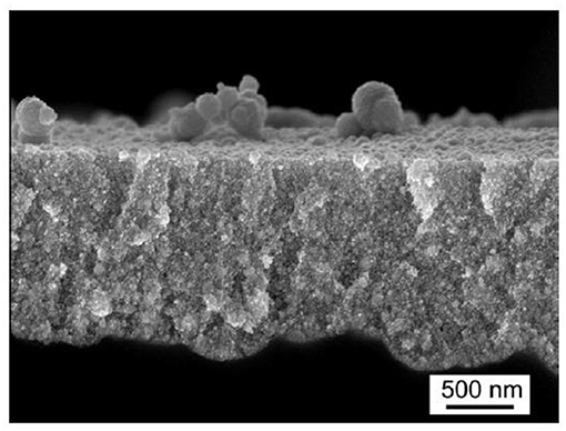
Figure 1. Cross-sectional SEM image of hydrophobic porous silicon filled with Pt. Fukami et al. [46], Elsevier by permission.
A further approach to fill porous structures is immersion plating. Immersion of as etched PSi into an 0.5 M CoCl2 solution for 120 min shows Co inside the pores with a concentration decrease toward the pore bottom [27]. Figure 2 shows the atomic percentage of Co in dependence on the porous layer thickness, obtained from EDX investigations.
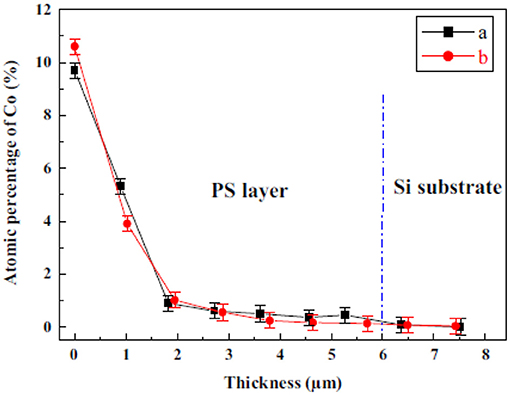
Figure 2. Depth dependence of the atomic percentage of Co obtained from EDX measurements showing (a) sample before temperature treatment and (b) after annealing at 400°C. Bouzouraa et al. [27], Elsevier by permission.
Ni deposition within microporous silicon has been performed in utilizing an aqueous 0.1 M NiCl2 solution. First a current density of 0.6 mAcm−2 has ben applied before the electroless deposition. The duration of the electroless reaction process was varied between 0 and 11 min [26]. Pulsed electrodeposition is employed to deposit Ni from the so-called Watts electrolyte consisting of NiCl2 (45 g/l) and NiSO4 (300 g/l) within porous silicon. A current density of 10 mAcm−2 and a frequency of 2 Hz has been applied. The deposition time has been enhanced from 5 till 15 min leading to a filling of the porous layer down to the bottom, which was evidenced by EDX spectra [47]. Figure 3 depicts an EDX spectrum taken at the pore tips [47].
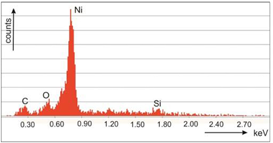
Figure 3. EDX-spectrum taken at the pore bottom of a cross-section of a Ni filled microporous silicon sample. Granitzer et al. [47], with permission.
Optical Properties of Microporous Silicon
Considering the photoluminescence of microporous silicon, the emission can be tuned due to the structure size in the region from the near-infrared to the ultraviolet in the case of a hydrogen passivated surface. Oxidation of the surface leads to a red shift of about 1 eV showing that quantum confinement and surface passivation, both determine the electronic states. This red-shift can be explained by recombination attendant to a trapped electron or exciton [48]. Since the quantum confinement model suggested by Canham [1] offers some deficiencies other models have been taken into account such as that the light emission comes from siloxane molecules formed on the surface [49] which could be disproved by thermal oxidation experiments [50]. A further approach to describe the luminescence is the surface states model, which involves the trapping and localization of photoexcited carriers in silicon related boundary states of the crystallites [51]. In the case of a structure size larger than 3 nm, offering a red/orange luminescence, the quantum confinement model is sufficient and surface passivation plays a minor role on the radiative recombination mechanism [48]. Radiative relaxation processes are influenced by quantum confinement and not affected by oxidation, whereas non-radiative relaxation processes are affected by the surface chemistry [52]. Continuous wavelength and time resolved photoluminescence of silicon nanocrystals embedded in a SiO2 matrix can be used to distinguish between microscopic and macroscopic characteristics of the decay [53]. Microscopic characteristics of the decay are attributed to quantum confinement effects and the macroscopic ones are affected by the environment of the silicon nanocrystal [53]. The decay results from two neighboring levels splitted in their energy and it has been found that the upper level decay is shorter (microseconds) than the lower level decay (milliseconds) [53]. Figure 4 depicts the slower triplet lifetimes which are due to the oxidation of the freshly prepared silicon and the faster singlet lifetimes which are not influenced by the surface chemistry as well as the energy splitting [52].
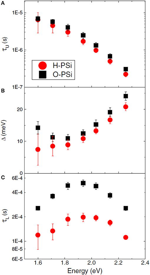
Figure 4. Comparison of hydrogen terminated and oxidized porous silicon, showing (A) upper singlet lifetimes, (B) excitonic energy splitting, and (C) lower triplet lifetimes. Arad-Vosk et al. [52], Springer with permission.
Metal filling of luminescent porous silicon can influence the optical properties of the material. The deposition of Au nanoparticles within the pores results in the excitation of surface plasmon polaritons and an increase of the photoluminescence intensity is observed [54]. Considering the interaction between porous silicon and Au nanoparticles on its surface, not only plasmon effects influence the optical properties but also the porosity and surface chemistry of the nanocomposite. The plasmonic behavior depends on the particle size and shape as well as on the refractive index of the surrounding medium. The latter one explains the dependence of the optical response on the porosity of the porous silicon [55]. The interaction of the plasmons of the Au nanoparticles with the excitons generated in the semiconductor result in a modification of the emission and absorption properties [56]. Considering the photoluminescence lifetime of an Au/PSi system, generally a decrease due to the plasmonic effects compared to plain PSi is expected. In [55] an increase of the decay times, which are determined by the fit of a stretched exponential, has been observed which could be explained by the surface chemistry of the samples. In the case of Au particles deposited on porous silicon nanowires an enhancement as well as a quenching of the photoluminescence intensity, depending on the deposition time and the solution concentration, has been reported [57]. An increase of the photoluminescence intensity and a blue shift of the spectrum has been reported in the case of silver nanoparticles positioned in the vicinity of silicon nanocrystals with a SiO2 spacer of a few nanometers in-between [58]. Figure 5 shows the comparison of the photoluminescence obtained from plain samples and samples containing Ag particles. The intensity increase can be explained by the coupling of the silicon nanocrystals to the surface plasmons of the Ag particles.
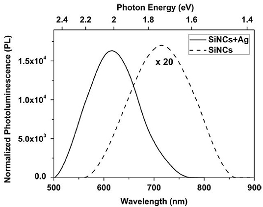
Figure 5. Photoluminescence spectra of only silicon nanocrystals (dashed line) and silicon nanocrystals with Ag particles deposited on the silicon surface (solid line). The latter case shows an increase of the luminescence intensity as well as a blue shift of the spectrum of about 100 nm. Gardelis et al. [58], Elsevier by permission.
An increase of the photoluminescence intensity could also be observed by electrodepositing Ag particles from an AgNO3 solution by varying the deposition time and the concentration of the electrolyte [59]. This behavior of the luminescence is furthermore shown after LiCl treatment of porous silicon as well as an enhancement of the minority carrier lifetime due to the passivation of the dangling bonds at the silicon surface [60].
The decay times obtained from time resolved measurements and fitting with a stretched exponential function show an increase of the recombination rate in the Ag particle loaded samples (Figure 6). Together with the enhanced photoluminescence, this is a hint that the Ag particles cause an increase of the emission rate of the silicon nanocrystals [58].
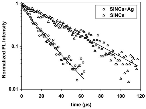
Figure 6. Comparison of the decay times of microporous samples containing Ag particles and samples without Ag. Gardelis et al. [58], Elsevier by permission.
The photoluminescence of porous silicon with incorporated Ni has been investigated with respect to the immersion time of the samples in an Ni-salt solution. An increase of the luminescence intensity has been observed with increasing immersion time from 1 to 7 min and a subsequent decrease of the intensity with further increasing immersion time. Furthermore, a blue shift of the spectrum has been measured [26]. Figure 7 depicts these findings. The photoluminescence intensity enhancement is explained by the reaction between the Ni ions and the porous silicon surface.
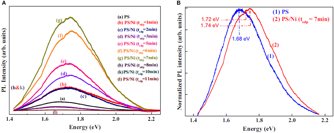
Figure 7. Photoluminescence spectra of Ni filled porous silicon in dependence on the immersion time. (A) Photoluminescence spectra for porous silicon and Ni/PSi for an immersion time from 1 to 11 min. (B) Normalized spectra showing the blue shift of Ni filled PSi (immersion time 7 min). Amdouni et al. [26], Elsevier by permission.
Stain etched porous silicon powder filled with Ni by electroless plating in a NiCl2 solution has been investigated concerning the photoluminescence of the composite system. The samples offer a dependence on the concentration of the NiCl2 solution (25–500 g/l). With increasing concentration the intensity decreases and increases again. The decreasing intensity behavior is explained by the increase of surface defects by the desorption of H-atoms forming a low quality oxide layer, the following increase of the intensity with higher concentration is due to the formation of a better quality oxide. The peak position of the photoluminescence spectrum also depends on the NiCl2 concentration. First a blue-shift is observed which could be caused by a reduction of the emitter size due to oxidation and with further increase of the concentration the wavelengths are red shifted [61].
In the case of using pulsed electrodeposition for the Ni filling of luminescent porous silicon the optical properties have been investigated in dependence on the deposition time, ranging from 5 to 15 min [47]. A small enhancement of the photoluminescence intensity and a blue-shift of the spectrum is observed with increasing deposition time. The decay times show a decrease from about 300 μs for bare porous silicon to about 100 μs for a metal filled sample (deposition time 15 min). This result can be interpreted by a decrease of the radiative lifetime. Generally radiative processes prevail the non-radiative processes at room temperature. The decay behavior of porous silicon can be explained by an excitonic two-level model with the upper excitonic singlet-triplet state and the ground state [52]. Coupling of the plasmonic modes of the Ni with the emitter (silicon) can occur due to the direct vicinity of the emitter and the deposited Ni, only separated by a native oxide layer, and lead to the increase of the photoluminescence intensity [47].
In contrast to the findings above, quenching of the photoluminescence has been reported after Co electrodeposition within porous silicon due to oxidation of the emitting centers. An additional blue emission band around 490 nm occurs due to silanol formation at the surface [62].
Magnetic Response Of Metal Filled Microporous Silicon
Filling of porous silicon with magnetic materials allows to tune the magnetic properties of the composite by the electrochemical deposition parameters as well as by the morphology of the porous silicon matrices. Considering luminescent porous silicon, due to the branched morphology also the metal deposits offer an interconnnected structure. Due to the pore-size (a few nanometers) the metal structures are in the superparamagnetic range but because of the interconnection between them ferromagnetic behavior is observed [47]. Microporous silicon filled with a magnetic material renders a system offering both, light emitting and magnetic properties and thus the nanocomposite is promising for magneto-optical on-chip devices. Temperature dependent magnetization measurement do not give any hint of superparamagnetism. In the case of isolated nanoparticles a clear peak showing the transition temperature between superparamagnetic behavior and blocked state would be observed. The investigated magnetic response strongly depends on the metal deposition time, which means the amount of metal inside the pores. An increase of the coercivity HC from 150 to 450 Oe with increasing deposition time from 5 to 15 min is observed (Figure 8A). In this case the magnetic field was applied parallel to the surface. Furthermore, the magnetic anisotropy between easy axis and hard axis magnetization shows a dependence on the filling time (Figure 8B). This anisotropic behavior is film-like and becomes more pronounced with increasing metal filling and thus more interconnections between the metal deposits. The magnetic easy axis corresponds to an external magnetic field applied parallel to the surface, which is in contrast to mesoporous silicon (see in section Optical Properties of Metal Filled Mesoporous Silicon). Two hysteresis curves, one measured with an applied field parallel and the other one with an applied field perpendicular to the sample surface are depicted in Figure 9.
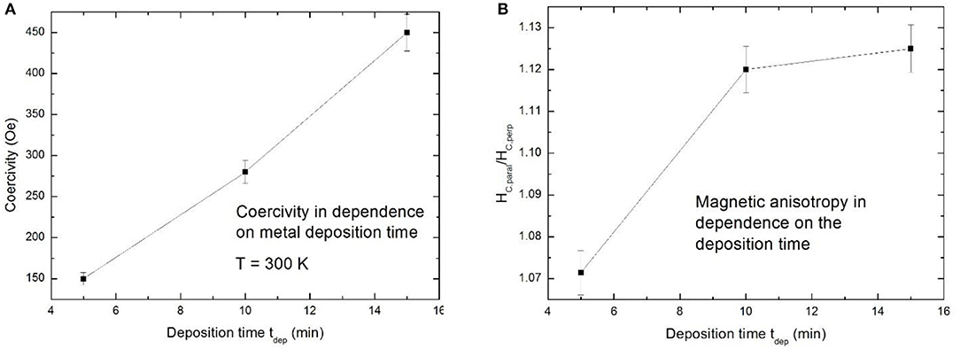
Figure 8. (A) Coercivity of microPSi/Ni in dependence on the deposition time. (B) Magnetic anisotropy (Hc, paral/Hc, perp) vs. filling time. Granitzer et al. [47], with permission.
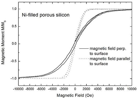
Figure 9. Field dependent magnetization curves measured with an applied field parallel (dotted line) and perpendicular (solid line) to the sample surface showing that the magnetic easy axis is parallel to the surface. Granitzer et al. [47], with permission.
The magnetic response of Ni deposited within porous silicon powder has been investigated with respect to the plating time and the concentration of the solution. The results show a superparamagnetic behavior, except for a plating time of 15 min. The measured magnetization increases with the plating time till a value of 360 min and afterwards decreases again [61]. Figure 10 shows the hysteresis for various plating times (a) and the normalized saturated magnetization in dependence on the deposition time (b) [61].
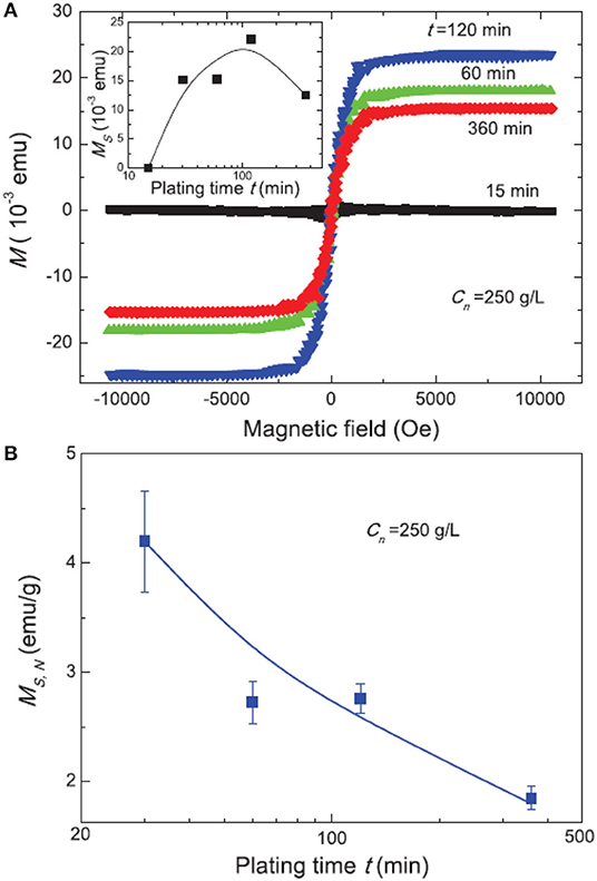
Figure 10. Field dependent magnetization curves of Ni/Psi in dependence on the deposition time (A) and normalized saturation magnetization in dependence on the deposition time (B). The inset in (A) shows the saturated magnetization vs. time. Reproduced from Nakamura et al. [61], with permission of AIP Publishing.
Also a non-superparamagnetic behavior has been observed for Co deposited within porous silicon particles, but all samples show a low coercivity [62] which indicates a low dispersion of Co within the porous structure offering only weak magnetic crosstalk.
Mesoporous Silicon
Mesoporous silicon offers in contrast to microporous silicon straight pores with more or less dendritic growth. The dendritic grows mainly depends on the electrochemical etching parameters such as applied current density, bath temperature and electrolyte concentration. Keeping the temperature and electrolyte concentration constant the regularity of the pore arrangement increases with increasing current density [63]. The dendrite-size and especially their length is determined by the distance between the pores. If this inter-pore distance exceeds twice the thickness of the space charge region the silicon skeleton is not any longer free of charge carriers which favors the formation of side pores [7]. The growth direction depends on the crystal orientation and this feature increases when the applied current density comes close to the critical current density at the pore tips. The fastest growth rate is along the (100) direction [7].
Fabrication and Metal Filling of Mesoporous Silicon
Mesoporous and macroporous silicon with pore diameters in the lower regime is generally fabricated in using a highly n- or p- doped silicon wafer. A standard formation procedure is anodic dissolution of bulk crystalline silicon in an aqueous hydrofluoric acid solution. In applying a high current density the breakthrough regime is enabled. In this case illumination of n-type silicon to generate holes for the silicon dissolution is not necessary. In the mesoporous regime straight self-organized nanoholes are formed. The pore diameter and the concomitant pore distance can be adjusted quite accurately by the electrochemical parameters.
A further common technique is stain etching, which means electroless etching of silicon in the presence of a solution generally containing acidic fluoride and an oxidant which injects holes into the valence band [64]. Using this electroless formation process it is more difficult to adjust the porous silicon morphology and the obtained porous layers are quite thin (few micrometers). In adding Fe3+, VO, or Ce4+ as oxidizing agent, thicker (>10 μm), more homogeneously and reproducible porous layers can be formed than with standard solutions [65].
Beside its large surface area, low electrical and thermal conductivity, mesoporous silicon can also offer photoluminescence in the visible range for structure sizes small enough for quantum confinement effects. Mesoporous silicon powder has been produced by anodization technique, subsequent detaching of the porous layer by applying a high current to exceed the critical current density, and finally hand milling of the detached porous layer. The samples were then treated by high pressure water vapor annealing for stabilization and to enhance the luminescence of the material [66].
In the following discussion porous silicon samples produced by anodization are considered. Since the morphology of the material can be tuned by the formation process, porous silicon is an adequate host material for pore filling. Beside attaching molecules to the surface for biomedical [67–69] or sensor [70–72] applications, the loading of the pores with metals has been investigated intensely. Requirements for this purpose are straight and separated pores to guarantee an arrangement of metal nanostructure arrays. The filling mechanism of different metals has been examined with the goal to control the metal deposition to produce tailored metal nanorods within the pores.
It has been reported that Fe deposition in low doped n-type silicon starts at the pore tips and grows along the walls. Mass transport limited conduction which accumulates electrons at the sample surface has been avoided in applying a low current density and in using a porous silicon morphology with wide pore opening [73]. Fe electrodeposition on p-type porous silicon is performed under cathodic conditions and under illumination, using n-type porous silicon, illumination can be omitted. Electron transfer reaction via the conduction band occurs in n-type porous silicon but in the case of p-type porous silicon electrons are generated by illumination [74]. Fe incorporated by electrodeposition within mesoporous silicon nucleates on the walls of the pores and on the surface. Generally the metal formation depends on the applied current density, pH of the electrolyte and the surface chemistry of the pore walls. Performing the deposition on an H-terminated porous silicon surface, Fe forms clusters at the surface. In using porous silicon with a native oxide layer Fe is deposited as randomly distributed particles within the pores [75]. Beside electrodeposition the Fe incorporation can also be performed by electroless deposition from the Fe salt solution [76].
Ni deposition can also be performed either electroless or electrochemically. In the case of immersion plating an aqueous ammonium fluoride solution containing NiSO4 is employed. Performing the deposition under room temperature metallic Ni is observed at the surface, whereas SiO2 is not detected [77]. Displacement deposition of Ni from an NiSO4, NH4F solution carried out at 60°C starts to grow at the pore walls rather than on the surface due to the Ni atoms mass transport toward the pore tips [78]. Displacement deposition of Ni produces a non-uniform deposition in high aspect ratio pores (~200) at the beginning of the reaction process due to a dominance of the mass transport. With increasing deposition time the Ni distribution along the pores becomes more uniform because the deposition rate decreases and the process is dominated by interfacial reaction [79].
In using electrodeposition for the metal filling of the pores, either dc or pulsed deposition can be employed. Pulsed electrodeposition under constant current density and applying rectangular pulses with a pulse duration of 1 s and a pulse delay time of 25 s is shown for different porous silicon porosities in Figure 11 [80]. The pulsed current deposition leads to nucleation of metal nanoparticles within the pores. A crucial parameter is the pulse delay time which can be estimated from the dynamics of the voltage vs. time graphs [81].
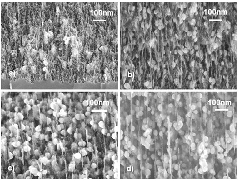
Figure 11. Cross-sectional scanning electron micrographs of porous silicon offering different morphologies with infiltrated Ni structures. The Ni deposition depends on the porous silicon porosity and it can be seen that for lower porosity the Ni particles are smaller than in the case of higher porosity. This behavior is due to faster exhaustion of the electrolyte and thus a longer growth time. Michelakaki et al. [80], Springer Nature with permission. In (a,b), the samples offer a porosity of about 70% and the Ni nanoparticle size is ~23 nm. With increasing porosity to 86% and 88% shown in (c,d), the Ni particle size increases to about 33 nm.
The shape of the metal deposits can be adjusted by the pulse-frequency and the applied current density. A variation of the frequency between 0.025 and 0.2 Hz results in a shape modification from spherical particles to elongated structures with an aspect ratio of about 100 [82]. In Figure 12 the dependence of the elongation of Ni structures on the pulse duration is depicted [83]. The spatial distribution of the deposits within the pores can be modified by the current density. Applying a current density between 5 and 25 mA/cm2, the packing density of the metal deposits within the pores can be modified by the pulse frequency. In the case of densely packed particles the time between the pulses is 5 s and for loosely packed particles it is 20 s [82].
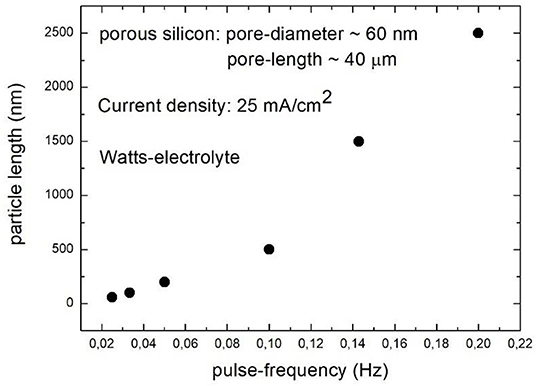
Figure 12. Pulse frequency vs. elongation of Ni deposits. With increasing pulse frequency the length of the Ni structures is increased. Granitzer et al. [83], ECS with permission.
In applying a current density of 25 mAcm−2 and a pulse frequency of 0.025 Hz more or less homogeneous deposition of spherical Ni particles with a moderate packing density is achieved and can be seen in Figure 13 [82].
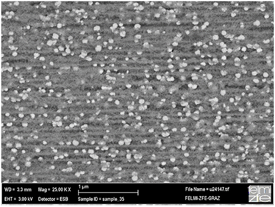
Figure 13. Cross-sectional back scattered electron micrograph (BSE) showing the distribution of sphere-like Ni deposits within porous silicon. Rumpf et al. [82], IOP with permission.
Optical Properties of Metal Filled Mesoporous Silicon
Not only from microporous but also from mesoporous silicon in the lowermost size regime luminescence can be observed. Furthermore, it can be utilized as template for metal particle deposition on the surface and act as SERS sensitive material. Mesoporous silicon produced by a standard chemical route, offering pore diameters of about 15 nm, and subsequent Ag particle deposition on its surface is shown to be Surface Enhanced Raman Scattering (SERS) active for rhodamine 6G and crystal violet. In using an excitation wavelength of 514.5 nm the rhodamine 6G and the silver plasmons are in resonance with the excitation light resulting in a large surface enhancement [84]. Ag nanoparticles deposited on porous silicon by immersing the sample into an AgNO3 solution are used for single molecule detection by SERS. The Raman response is investigated in employing Cyanine and Rhodamine 6G. If the particle plasmon resonance coincides with the molecule electronic resonance strong Raman enhancement is observed [85]. The utilization of mesoporous silicon as template material in comparison to microporous silicon for Ag particle deposition shows a broader particle size distribution as well as a localized surface plasmon resonance closer to the excitation wavelength. Due to the high SERS sensitivity ultralow concentrations of dye molecules can be detected [86]. Furthermore, Ag nanostructures in SiO2/p-silicon is found as SERS active substrate in a broad spectral range [87]. Au nanoparticles modified porous silicon shows a strong fluorescence enhancement due to plasmon resonance which is used for highly sensitive DNA detection [88]. Porous silicon with a Au nanoparticle layer on top offers light absorption by the Au particles leading to localized surface plasmon resonance. The wavelength of the plasmon resonance depends not only on the Au nanostructures but also on the refractive index of the surrounding medium. Plasmon resonance is sensitive to changes in the refractive index only close to the dielectric/metal interface [89]. Metal decorated porous silicon structures are feasible as sensors, especially to detect molecules.
Magnetic Response of Metal Filled Mesoporous Silicon
Mesoporous silicon with its tunable morphology by the formation parameters, its straight pores and its quasi regular pore arrangement is an adequate system to embedded magnetic nanostructures and to adjust the resulting magnetic properties. On the one hand the magnetic response strongly depends on the size, shape and distribution of the metal deposits and on the other hand the morphology of the porous silicon plays a crucial role, especially with respect to magnetic interactions between deposits of adjacent pores. The magnetic response of the nanocomposite samples allows to draw conclusions from the shape of the deposits. The coercivity HC decreases with the elongation of the embedded metal structures whereas the reduced remanence (magnetic remanence MR/saturation magnetization MS) increases with increasing elongation approaching a wire-like behavior [90], summarized in Table 1.
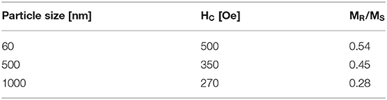
Table 1. Dependence of the coercivity HC on the particle elongation.
Furthermore, the packing density of the metal deposits within the pores influences the magnetic characteristics. Densely packed metal particles magnetically interact within the pores leading to a wire like behavior and thus to a smaller coercivity compared to isolated particles with comparable size. Field dependent magnetization measurements performed at various temperatures ranging from 4 to 300 K shows that the coercivity decreases with increasing temperature [91]. Some values for T = 4,100, and 250 K are depicted in Table 2.
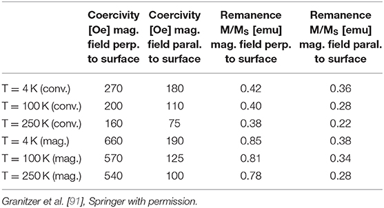
Table 2. Magnetic features measured at T = 4, 100 K and T = 250 K summarized for conventional etched samples and magnetic field assisted etched ones.
The magnetic response is also strongly influenced by the morphology of the porous silicon template, especially regarding the dendritic pore growth [92]. A reduction of the side pore growth could be achieved by magnetic field assisted etching, in applying a magnetic field of 8 T perpendicular to the sample surface during the anodization process [93]. With increasing side pore length the effective mean distance between the pores decreases resulting in stronger magnetic cross talk between metal deposits within adjacent pores. A further important parameter is beside the dendritic pore growth, the roughness of the pores because the embedded metal deposits grow with concomitant morphology. In the case of occurrence of side pores the metal deposits offer strong roughness which results in magnetic stray fields, influencing the magnetic response and reducing the coercivity of the nanocomposite [92]. Performing magnetization measurements with an applied field parallel and perpendicular to the sample surface one sees that the magnetic easy axis corresponds to the pore direction. The magnetic anisotropy between these two magnetization directions increases with increasing length of the metal deposits and with decreasing magnetic interactions between structures of neighboring pores. Figure 14 shows the magnetic anisotropy for magnetic field assisted etched porous silicon with elongated Ni structures deposited within the pores.
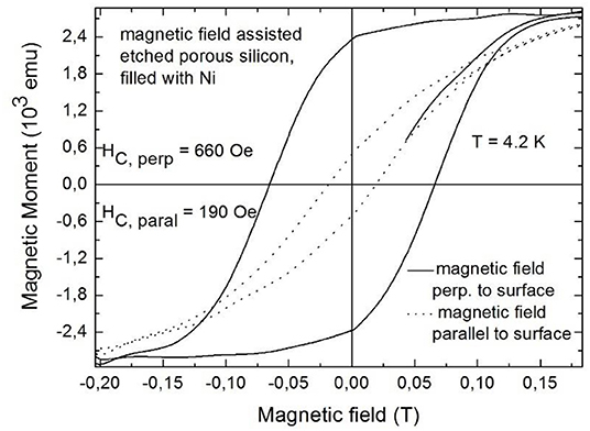
Figure 14. Magnetic field dependent measurements performed with an external field applied perpendicular (solid line) and parallel (dotted line) to the sample surface. Granitzer et al. [94], AIP with permission.
Considering Fe deposits within porous silicon, in and out of plane magnetization measurements show a magnetic anisotropy originating from the elongated shape of the deposits [75]. The easy axis corresponds to the pore direction with a reduced remanence (MR/MS) of 0.6 [75] which is a typical value for such nanocomposites including magnetic cross talk.
These investigations show that control of the porous silicon formation resulting in more or less ordered pores with a minimum on roughness are a precondition to suppress magnetic coupling between the deposited metal structures of adjacent pores. By adjusting the metal deposition parameters accurately desired size and shape of the deposited nanostructures can be obtained.
Conclusions
In this work the utilization of porous silicon in the microporous and mesoporous regime as template material for metal deposition has been discussed. The optical properties such as the luminescence and the associated decay times of microporous silicon have been addressed also with respect to metal filling of these templates which modifies and improves the light emission. The plasmon resonance of the deposited metal structures can be exploited to enhance the luminescence and in combination with dye molecules the system can act as active SERS material. Due to the employment of magnetic metals nanocomposites with adjusted magnetic features strongly correlated to the size, shape, and distribution of the deposits can be achieved. In the case of microporous silicon optical and magnetic properties are merged on one material level which makes the system interesting for magneto-optical applications. A further key parameter concerning the magnetic features is the morphology of the porous silicon, especially the distance between the pores which is strongly influenced by dendritic pore growth. A reduction of the side pore length results in a decrease of the magnetic crosstalk and thus approaches the magnetic characteristics of individual magnetic nanostructures. Since these nanocomposites offer a silicon substrate which is applicable in today's microtechnology the discussed systems are promising to act as component in on-chip devices.
Author Contributions
PG and KR wrote this review article and they are responsible for the content of the work.
Conflict of Interest
The authors declare that the research was conducted in the absence of any commercial or financial relationships that could be construed as a potential conflict of interest.
References
1. Canham L. Silicon quantum wire array fabrication by electrochemical and chemical dissolution of wafers. Appl Phys Lett. (1990) 57:1046. doi: 10.1063/1.103561
2. Kolasinski KW. New approaches to the production of porous silicon by stain etching. In: Granitzer P, Rumpf K, editors. Nanostructured Semiconductors - From Basic Research to Applications. Singapore: Pan Stanford Publishing (2014). p. 45–72.
3. Chartier C, Bastide S, Levy-Clement C. Metal-assisted chemical etching of silicon in HF-H2O2. Electrochim Acta. (2008) 53:5509–16. doi: 10.1016/j.electacta.2008.03.009
4. Kolasinski KW. The mechanism of galvanic/metal-assisted etching of silicon. Nanoscale Res Lett. (2014) 9:432. doi: 10.1186/1556-276X-9-432
5. Gianneta V, Olziersky A, Nassiopoulou AG. Si nanopatterning by reactive ion etching through an on-chip self-assembled porous anodic alumina mask. Nanoscale Res Lett. (2013) 8:71. doi: 10.1186/1556-276X-8-71
6. Zhang J, Zhao L, Rosenkranz A, Song C, Yan Y, Sun T. Nanosecond pulsed laser ablation of silicon-finite element simulation and experimental validation. J Micromech Microeng. (2019) 29:075009. doi: 10.1088/1361-6439/ab208b
7. Lehmann V. Electrochemistry of Silicon - Instrumentation, Science, Materials and Applications. Weinheim: Wiley-VCH (2002).
8. Herino R, Bomchil G, Barla K, Bertrand C, Ginoux JL. Porosity and pore size distributions of porous silicon layers. J Electrochem Soc. (1987) 134:1994. doi: 10.1149/1.2100805
9. Herino R. Pore size distribution in porous silicon. In: Canham LT, editor. Properties of Porous Silicon. London: INSPEC (1997). p. 89–97.
10. Cullis AG, Canham LT. Visible light emission due to quantum size effects in highly porous crystalline silicon. Nature. (1991) 353:335. doi: 10.1038/353335a0
11. Lehmann V, Jobst B, Muschik T, Kux A, Petrova-Koch V. Correlation between optical properties and crystallite size in porous silicon. Jpn J Appl Phys. (1993) 32:2095. doi: 10.1143/JJAP.32.2095
12. Zeman J, Zigone M, Rikken GLJA, Martinez G. Hydrostatic pressure effects on the porous silicon luminescence. J Phys Chem Solids. (1995) 56:655–61. doi: 10.1016/0022-3697(94)00259-2
13. Fauchet PM, Tsybeskov L, Peng C, Duttagupta SP, von Behren J, Kostoulas Y, et al. Light-emitting porous silicon: materials science, properties, and device applications. IEEE J Select Top Quant Electron. (1995) 1:1126. doi: 10.1109/2944.488691
14. Canham LT. Luminescence bands and their proposed origins in highly porous silicon. Phys Stat Sol. (1995) 190:9. doi: 10.1002/pssb.2221900102
15. Mauckner G, Hamann J, Rebitzer W, Baier T, Thonke K, Sauer R. Origin of the infrared band from porous silicon. Mater Res Soc Symp Proc. (1995) 358:489. doi: 10.1557/PROC-358-489
16. Li P, Wang G, Ma Y, Fang R. Origin of the blue and red photoluminescence from aged porous silicon. Phys Rev B. (1998) 58:4057. doi: 10.1103/PhysRevB.58.4057
17. Grivickas V, Linnros J. Free-carrier absorption and luminescence decay of porous silicon. Thin Solid Films. (1995) 255:70–3. doi: 10.1016/0040-6090(94)05606-E
18. Trojanek F, Maly P, Pelant I, Hospodkova A, Kohlova V, Valenta J. Picosecond dynamics of photoexcited carriers in free-standing porous silicon. Thin Solid Films. (1995) 255:77–9. doi: 10.1016/0040-6090(94)05610-P
19. M'Ghaleth R, Maaref H, Mihalcescu I, Vial JC. Porous silicon: photoluminescence decay in the nanosecond range. Microelectron J. (1999) 30:695–8. doi: 10.1016/S0026-2692(99)00013-0
20. Joo J, Defforge T, Loni A, Kim D, Li ZY, Sailor MJ, et al. Enhanced quantum yield of photoluminescent porous silicon prepared by supercritical drying. Appl Phys Lett. (2016) 108:153111. doi: 10.1063/1.4947084
21. Gelloz B, Juangsa FB, Nozaki T, Asaka K, Koshida N, Jin L. Si/SiO2 core/shell luminescent silicon nanocrystals and porous silicon powders with high quantum yield, long lifetime, and good stability. Front Phys. (2019) 7:47. doi: 10.3389/fphy.2019.00047
22. Koshida N, Koyama H. Visible electroluminescence from porous silicon. Appl Phys Lett. (1992) 60:347. doi: 10.1063/1.106652
23. Lehmann V, Hofmann F, Möller F, Grüning U. Resistivity of porous silicon: a surface effect, Thin Solid Films. (1995) 255:20. doi: 10.1016/0040-6090(94)05624-M
24. Herino R. Impregnation of porous silicon. In: Canham L, editor. Properties of Porous Silicon. London: INSPEC (1997). p. 66–77.
25. Rahmani M, Moadhen A, Zaibi MA, Elhouichet H, Oueslati M. Photoluminescence enhancement and stabilisation of porous silicon passivated by iron. J Lumin. (2008) 128:1763–6. doi: 10.1016/j.jlumin.2008.04.003
26. Amdouni S, Rahmani M, Zaibi MA, Oueslati M. Enhancement of porous silicon photoluminescence by electroless deposition of nickel. J Lumin. (2015) 157:93–7. doi: 10.1016/j.jlumin.2014.08.041
27. Bouzouraa MB, Rahmani M, Zaibi MA, Lorrain N, Hajji L, Oueslati M. Optical study of annealed cobalt-porous silicon nanocomposites. J Lumin. (2013) 143:521–5. doi: 10.1016/j.jlumin.2013.05.050
28. Lublow M, Kubala S, Veyan JF, Chabal YJ. Colored porous silicon as support for plasmonic nanoparticles. J. Appl. Phys. (2012) 111:084302. doi: 10.1063/1.3703469
29. Lehmann V, Stengl R, Luigart A. On the morphology and the electrochemical formation mechanism of mesoporous silicon. Mater Sci Eng B. (2000) 69–70:11–22. doi: 10.1016/S0921-5107(99)00286-X
30. Granitzer P, Rumpf K, Pölt P, Albu M, Chernev B. The interior interfaces of a semiconductor/metal nanocomposite and their influence on its physical properties. Phys Stat Sol. (2009) 6:2222–7. doi: 10.1002/pssc.200881730
31. Granitzer P, Rumpf K, Ohta T, Koshida N, Poelt P, Reissner M. Magnetic field assisted etching of porous silicon as a tool to enhance magnetic characteristics. ECS Trans. (2013) 50:55. doi: 10.1149/05037.0055ecst
32. Uhlir A Jr. Electrolytic shaping of germanium and silicon. Bell System Tech J. (1956) 35:333–47. doi: 10.1002/j.1538-7305.1956.tb02385.x
33. Ram SK. Electrical transport in porous silicon. In: Canham LT, editor. Handbook of Porous Silicon. Cham: Springer (2018). p. 263–79.
34. Zhao Y, Yang L, Kong L, Nai MH, Liu D, Wu J, et al. Ultralow thermal conductivity of single-crystalline porous silicon nanowires. Adv Func Mater. (2017) 27:1702824. doi: 10.1002/adfm.201702824
35. Sohn H. Refractive index of porous silicon. In: Canham LT, editor. Handbook of Porous Silicon. Cham: Springer (2018). p. 231–43.
36. Fujii M, Diener J. Optical birefringence of porous silicon. In: Canham LT, editor. Handbook of Porous Silicon. Cham: Springer (2018). p. 245–53.
37. Canham L. Mechanical properties of porous silicon. In: Canham LT, editor. Handbook of Porous Silicon. Cham: Springer (2018). p. 213–20.
38. Lehmann V, Grüning U. The limits of macropore array fabrication. Thin Solid Films. (1997) 297:13. doi: 10.1016/S0040-6090(96)09478-3
39. Lehmann V, Rönnebeck S. The physics of macropore formation in low-doped p-type silicon. J Electrochem Soc. (1999) 146:2968. doi: 10.1149/1.1392037
40. Halimaoui A. Determination of the specific surface area of porous silicon from its etch rate in HF solutions. Surf Sci Lett. 306:L550–4 (1994). doi: 10.1016/0039-6028(94)91176-2
41. Kolasinski K. Porous silicon formation by stain etching. In: Canham LT, editor. Handbook of Porous Silicon. Cham: Springer (2018). p. 35–48.
42. Kolasinski K, Yadlovskiy J. Stain etching of silicon with V2O5. Phys Stat Sol. (2011) 8:1749–53. doi: 10.1002/pssc.201000063
43. Ossicini S, Pavesi L, Priolo F. Light Emitting Silicon for Microphotonics. Berlin: Springer (2003).
44. Koda R, Fukami K, Sakka T, Ogata YH. A physical mechanism for suppression of zinc dendritescaused by high efficiency of the electrodeposition within confined nanopores. ECS Electrochem Lett. 2:D9 (2013). doi: 10.1149/2.010302eel
45. Koda R, Fukami K, Sakka T, Ogata YH. Electrodeposition of platinum and silver into chemically modified microporous silicon electrodes. Nanoscale Res Lett. (2012) 7:330. doi: 10.1186/1556-276X-7-330
46. Fukami K, Koda R, Sakka T, Urata T, Amano K, Takaya H, et al. Platinum electrodeposition in porous silicon: the influence of surface solvation effects on a chemical reaction in a nanospace. Chem Phys Lett. (2012) 542:99–105. doi: 10.1016/j.cplett.2012.05.078
47. Granitzer P, Rumpf K, Poelt P, Reissner M. Magnetic characteristics of Ni-filled luminescent porous silicon. Front Chem. (2019) 7:41. doi: 10.3389/fchem.2019.00041
48. Wolkin MV, Jorne J, Fauchet PM, Allan G, Delerue C. Electronic states and luminescence in porous silicon quantum dots: the role of oxygen. Phys Rev Lett. (1999) 82:197. doi: 10.1103/PhysRevLett.82.197
49. Brandt MS, Fuchs HD, Stutzmann M, Weber J, Cardona M. The origin of visible luminescencefrom “porous silicon”: a new interpretation. Solid State Commun. (1992) 81:307–12. doi: 10.1016/0038-1098(92)90815-Q
50. Petrova-Koch V, Muschik T, Kux A, Meyer BK, Koch F, Lehmann V. Rapid-thermal-oxidized porous Si–the superior photoluminescent Si. Appl Phys Lett. (1992) 61:943. doi: 10.1063/1.107736
51. Koch F, Petrova-Koch V, Muschik T. The luminescence of porous Si: the case for the surface state mechanism. J Lumin. (1993) 57:271–81. doi: 10.1016/0022-2313(93)90145-D
52. Arad-Vosk N, Sa'ar A. Radiative and nonradiative relaxation phenomena in hydrogen- and oxygen-terminated porous silicon. Nanoscale Res Lett. (2014) 9:47. doi: 10.1186/1556-276X-9-47
53. Dovrat M, Goshen Y, Jedrzejewski J, Balberg I, Sa'ar A. Radiative versus nonradiative decay processes in silicon nanocrystals probed by time-resolved photoluminescence spectroscopy. Phys Rev B. (2004) 69:155311. doi: 10.1103/PhysRevB.69.155311
54. Vainshtein JS, Goryachev DN, Ken OS, Sreseli OM. Surface plasmon polaritons in a composite system of porous silicon and gold. Semiconductors. (2015) 49:442–7. doi: 10.1134/S1063782615040260
55. de la Mora MB, Bornacelli J, Nava R, Zanella R, Reyes-Esqueda JA. Porous silicon photoluminescence modification by colloidal gold nanoparticles: plasmonic, surface and porosity roles. J Lumin. (2014) 146:247–55. doi: 10.1016/j.jlumin.2013.09.053
56. Achermann M. Exciton–plasmon interactions in metal–semiconductor nanostructures. J Phys Chem Lett. (2010) 1:2837. doi: 10.1021/jz101102e
57. Tang H, Liu C, He H. Surface plasmon enhanced photoluminescence from porous silicon nanowires decorated with gold nanoparticles. RCS Adv. (2016) 6:59395. doi: 10.1039/C6RA06019F
58. Gardelis S, Gianneta V, Nassiopoulou AG. Twenty-fold plasmon-induced enhancement of radiative emission rate in silicon nanocrystals embedded in silicon dioxide. J Lumin. (2016) 170:282–7. doi: 10.1016/j.jlumin.2015.10.029
59. Cetinel A, Artunc N, Tarhan E. The growth of silver nanostructures on porous silicon for enhanced photoluminescence: the role of AgNO3 concentration and deposition time. Eur Phys J Appl Phys. (2019) 86:11301. doi: 10.1051/epjap/2019190013
60. Azaiez K, Zaghouani RB, Khamlich S, Meddeb H, Dimassi W. Enhancement of porous silicon photoluminescence property by lithium chloride treatment. Appl Surf Sci. (2018) 441:272–6. doi: 10.1016/j.apsusc.2018.02.006
61. Nakamura T, Adachi S. Properties of magnetic nickel/porous-silicon composite powders. AIP Adv. (2012) 2:032167. doi: 10.1063/1.4754152
62. Munoz-Noval A, Sanchez-Vaquero V, Torres-Costa V, Gallach D, Ferro-Llanos V, Serrano JJ, et al. Hybrid luminescent/magnetic nanostructured porous silicon particles for biomedical applications. J Biomed Optics. (2011) 16:025002. doi: 10.1117/1.3533321
63. Granitzer P, Rumpf K. Mesoporous silicon utilized as matrix for 3-dimensional arrays of ferromagnetic nanostructures. In: Burness LT, editor. Mesoporous Materials: Properties, Preparation and Applications. New York, NY: Nova Science Publishing (2009). p. 99–120.
64. Nahidi M, Kolasinski KW. Effects of stain etchant composition on the photoluminescence and morphology of porous silicon. J Electrochem Soc. (2006) 153:C19 (2006). doi: 10.1149/1.2129558
65. Kolasinski KW. Charge transfer and nanostructure formation during electroless etching of silicon. J Phys Chem C. (2010) 114:22098. doi: 10.1021/jp108169b
66. Gelloz B, Loni A, Canham L, Koshida N. Luminescence of mesoporous silicon powders treated by high-pressure water vapor annealing. Nanoscale Res Lett. (2012) 7:382. doi: 10.1186/1556-276X-7-382
67. Rodriguez GA, Lawrie JL, Weiss SM. Nanoporous silicon biosensors for DNA sensing. In: Santos HA, editor. Porous Silicon for Biomedical Applications. Cambridge: Woodhead Publishing (2014). p. 304–33.
68. Kim B, Sun S, Varner JA, Howell SB, Ruoslahti E, Sailor MJ. Securing the payload, finding the cell, and avoiding the endosome: peptide-targeted, fusogenic porous silicon nanoparticles for delivery of siRNA. Adv Mater. (2019) 31:1902952. doi: 10.1002/adma.201902952
69. Tieu T, Alba M, Elnathan R, Cifuetes-Rius A, Voelcker NH. Advances in porous silicon-based nanomaterials for diagnostic and therapeutic applications. Adv Therap. (2019) 2:1800095. doi: 10.1002/adtp.201800095
70. De Stefano L. Porous silicon optical biosensors: still a promise or a failure? Sensors. (2019) 19:4776. doi: 10.3390/s19214776
71. Barillaro G. Porous silicon gas sensing. In: Canham LT, editor. Handbook of Porous Silicon. Cham: Springer (2018). p. 845–56.
72. Ozdemir S, Gole JL. The potential of porous silicon gas sensors. Curr Opin Solid State Mater Sci. (2007) 11:92. doi: 10.1016/j.cossms.2008.06.003
73. Renaux C, Scheuren V, Flandre D. New experiments on the electrodeposition of iron in porous silicon. Microelectron Reliabil. (2000) 40:877–9. doi: 10.1016/S0026-2714(99)00331-5
74. Harraz FA, Sakka T, Ogata YH. A comparative electrochemical study of iron deposition onto n- and p-type porous silicon prepared from lightly doped substrates. Electrochim Acta. (2005) 50:5340–8. doi: 10.1016/j.electacta.2005.03.013
75. Bardet B, Defforge T, Negulescu B, Valente D, Billoue J, Poveda P, et al. Shape-controlled electrochemical synthesis of mesoporous Si/Fe nanocomposites with tailored ferromagnetic properties. Mater Chem Front. (2017) 1:190. doi: 10.1039/C6QM00040A
76. Miu M, Kleps I, Ignat T, Simion M, Bragaru A. Study of nanocomposite iron/porous silicon material. J Alloys Compounds. (2010) 496:265–8. doi: 10.1016/j.jallcom.2010.01.058
77. Harraz FA, Sasano J, Sakka T, Ogata YH. Different behavior in immersion plating of nickel on porous silicon from acidic and alkaline fluoride media. J Electrochem Soc. (2003) 150:C277. doi: 10.1149/1.1562595
78. Xu C, Zhang X, Tu K-N, Xie Y. Nickel displacement deposition of porous silicon with ultrahigh aspect ratio. J Electrochem Soc. (2007) 154:D170. doi: 10.1149/1.2430690
79. Xu C, Li M, Zhang X, Tu K-N, Xie Y. Theoretical studies of displacement deposition of nickel into porous silicon with ultrahigh aspect ratio. Electrochim Acta. (2007) 52:3901–9. doi: 10.1016/j.electacta.2006.11.007
80. Michelakaki E, Valalaki K, Nassiopoulou AG. Mesoscopic Ni particles and nanowires by pulsed electrodeposition into porous Si. J Nanopart Res. (2013) 15:1499. doi: 10.1007/s11051-013-1499-3
81. Munoz-Noval A, Gallach D, Garcia MA, Ferro-Llanos V, Herrero P, Fukami K, et al. Characterization of hybrid cobalt-porous silicon systems: protective effect of the matrix in the metal oxidation. Nanoscale Res Lett. (2012) 7:495. doi: 10.1186/1556-276X-7-495
82. Rumpf K, Granitzer P, Hilscher G, Pölt P. Interacting low dimensional nanostructures within a porous silicon template. J Phys Conf Ser. (2011) 303:012048. doi: 10.1088/1742-6596/303/1/012048
83. Granitzer P, Rumpf K, Koshida N, Pölt P, Michor H. Electrodeposited metal nanotube/nanowire arrays in mesoporous silicon and their morphology dependent magnetic properties. ECS Trans. (2014) 58:139. doi: 10.1149/05832.0139ecst
84. Zeiri L, Rechav K, Porat Z, Zeiri Y. Silver nanoparticles deposited on porous silicon as a surface-enhanced raman scattering (SERS) active substrate. Appl Spectr. (2012) 66:294–9. doi: 10.1366/11-06476
85. Virga A, Rivolo P, Frascella F, Angelini A, Descrovi E, Geobaldo F, et al. Silver nanoparticles on porous silicon: approaching single molecule detection in resonant SERS regime. J Phys Chem C. (2013) 117:20139. doi: 10.1021/jp405117p
86. Kosovic M, Balarin M, Ivanda M, Derek V, Marcius M, Ristic M, et al. Porous silicon covered with silver nanoparticles as surface-enhanced raman scattering (SERS) substrate for ultra-low concentration detection. Appl Spectr. (2015) 69:1417. doi: 10.1366/14-07729
87. Yakimchuk D, Kaniukov E, Bundyukova V, Osminkina L, Teichert S, Demyanov S, et al. Silver nanostructures evolution in porous SiO2/p-Si matrices for wide wavelength surface-enhanced Raman scattering applications. MRS Commun. (2018) 8:95. doi: 10.1557/mrc.2018.22
88. Wang J, Jia Z. Metal nanoparticles/porous silicon microcavity enhanced surface plasmon resonance fluorescence for the detection of DNA. Sensors. (2018) 18:661. doi: 10.3390/s18020661
89. Balderas-Valadez RF, Schürmann R, Pacholski C. One spot-two sensors: porous silicon interferometers in combination with gold nanostructures showing localized surface plasmon resonance. Front Chem. (2019) 7:593. doi: 10.3389/fchem.2019.00593
90. Rumpf K, Granitzer P, Koshida N, Poelt P, Reissner M. Magnetic interactions between metal nanostructures within porous silicon. Nanoscale Res Lett. (2014) 9:412. doi: 10.1186/1556-276X-9-412
91. Granitzer P, Rumpf K, Ohta T, Koshida N, Poelt P, Reissner M. Porous silicon/Ni composites of high coercivity due to magnetic field-assisted etching. Nanoscale Res Lett. (2012) 7:384. doi: 10.1186/1556-276X-7-384
92. Rumpf K, Granitzer P, Koshida N, Pölt P, Michor H. Morphology controlled magnetic interactions in metal embedded porous silicon nanostructures. ECS J Solid State Sci Technol. (2015) 4:N41. doi: 10.1149/2.0221505jss
93. Hippo D, Nakamine Y, Urakawa K, Tsuchiya Y, Mizuta H, Koshida N, et al. Formation mechanism of 100-nm-scale periodic structures in silicon using magnetic-field-assisted anodization. Jpn J Appl Phys. (2008) 47:7398. doi: 10.1143/JJAP.47.7398
Keywords: porous silicon, electrodeposition, magnetic nanostructures, luminescence, magnetic properties
Citation: Granitzer P and Rumpf K (2020) Metal Filled Nanostructured Silicon With Respect to Magnetic and Optical Properties. Front. Phys. 8:121. doi: 10.3389/fphy.2020.00121
Received: 18 February 2020; Accepted: 26 March 2020;
Published: 24 April 2020.
Edited by:
Simona Binetti, University of Milano-Bicocca, ItalyReviewed by:
Tatiana S. Perova, Trinity College Dublin, IrelandShinji Yae, University of Hyogo, Japan
Copyright © 2020 Granitzer and Rumpf. This is an open-access article distributed under the terms of the Creative Commons Attribution License (CC BY). The use, distribution or reproduction in other forums is permitted, provided the original author(s) and the copyright owner(s) are credited and that the original publication in this journal is cited, in accordance with accepted academic practice. No use, distribution or reproduction is permitted which does not comply with these terms.
*Correspondence: Petra Granitzer, cGV0cmEuZ3Jhbml0emVyJiN4MDAwNDA7dW5pLWdyYXouYXQ=