
95% of researchers rate our articles as excellent or good
Learn more about the work of our research integrity team to safeguard the quality of each article we publish.
Find out more
ORIGINAL RESEARCH article
Front. Phys. , 05 May 2020
Sec. Condensed Matter Physics
Volume 8 - 2020 | https://doi.org/10.3389/fphy.2020.00115
 A. M. Alsaad1*
 Qais M. Al-Bataineh1
 I. A. Qattan2
 Ahmad A. Ahmad1
 A. Ababneh3,4
 Zaid Albataineh3
 Ihsan A. Aljarrah1
 Ahmad Telfah5
We report our results on highly textured aluminum nitride (AlN) thin films deposited on glass substrates, oriented along the c-axis, using DC-magnetron sputtering technique for different values of back pressure. The structural, electronic, optical, piezoelectric, dielectric, and elastic properties of sputtered AlN thin films are measured and characterized. In particular, X-ray powder diffraction (XRD) technique shows that AlN thin films exhibit a hexagonal structure. Moreover, we employed ab initio simulations of AlN using the Vienna Ab Initio Simulation Package (VASP) to investigate the structural and the electronic properties of hexagonal AlN structures. The experimental lattice parameters of the as-prepared thin films agree well with those calculated using the total energy minimization approach. The optical parameters of AlN thin films, such as transmittance and refractive index, were measured using UV–vis measurements. Our measurements of refractive index, n, of AlN thin films yield a value of 2.2. Furthermore, the elastic, piezoelectric, and dielectric tensors of AlN crystal are calculated using VASP. The dynamical Born effective charge tensor is reported for all atoms in the unit cell of AlN. Interestingly, ab initio simulations indicate that AlN has a static dielectric constant approximately equal to 4.68, which is in good agreement with the reported experimental value. In addition, the clamped-ion piezoelectric tensor is calculated. The diagonal components of the piezoelectric tensor are found to be and . The large values of the piezoelectric coefficients show that a polar AlN crystal exhibits a strong microwave piezoelectric effect. Additionally, the components of the elastic moduli tensor are calculated. The extraordinary electronic, optical, piezoelectric, and elastic properties make AlN thin films potential candidates for several optoelectronic, elastic, dielectric, and piezoelectric applications.
Aluminum nitride (AlN), in its ground state, crystallizes in a hexagonal close-packed wurtzite structure [1]. AlN thin films have attracted much interest owing to the fact that they have unique features and a wide range of technological applications in various fields such as pressure sensors [2], energy harvesters [3], surface acoustic wave devices [4], and light-emitting devices [5] due to their noticeable large piezoelectric coefficients, d31 and d33 [6, 7], good electrical isolation [8, 9], wide band gap [10, 11], and high acoustic wave velocity [12, 13]. Additionally, AlN thin films have an exceptional blend of physical, elastic, and chemical properties. AlN exhibits extraordinary optical properties such as large optical band gap energy, ~6.2 eV, and large refractive index, ~2.0. Furthermore, it has interesting electronic, thermal, dielectric, and electronic properties such as extremely high electric resistivity (1014 Ω), high thermal conductivity (320 W/m K), large stiffness [14], and high dielectric constant. A bulk of AlN single crystals that are selectively oriented in the c-plane has been synthesized and reported to have a large acoustic wave velocity [15]. The abovementioned interesting properties attracted the attention of several research groups to explore AlN for the fabrication of piezoelectric and optoelectronic devices.
Thin films have been grown by several techniques. Methods such as reactive molecular beam epitaxy [16], pulsed laser deposition [17], DC/RF reactive sputtering [18, 19], vacuum arc/cathodic arc deposition [20], ion beam sputtering [21], miscellaneous [22], and sol-gel technique [23] have been implemented to grow AlN thin films of different sizes. The advantage of using reactive sputtering process over the other techniques to synthesize AlN thin films is obtaining films oriented along the c-axis and deposited at room temperature with large piezoelectric coefficients [24, 25].
In this work, we analyze the structural properties of AlN thin films deposited on a glass substrate synthesized by DC-magnetron sputtering technique relative to back pressures. This is an important step to determine the optimum back associated with the equilibrium lattice parameters of AlN thin films. For the sake of comparison, total energy minimization approach embedded in Vienna Ab Initio Simulation Package (VASP) is used to obtain the optimized lattice parameters. We found that the experimental and the calculated lattice parameters are in excellent agreement. Furthermore, we investigate the effect of back power on the refractive index and the optical band gap energy of AlN thin films. Theoretically, we present first-principle results on lattice dynamics and the dielectric, piezoelectric, and mechanical properties of AlN to find the interplay between these properties and the potential of this novel material for the current and the next generation of modern devices.
We prepare AlN thin films of thickness of 550 nm. The as-prepared thin films were deposited on glass substrates. The glass substrate was pre-etched and cleaned in acetone and deionized water in a (Ardenne-LS 730 S) DC-magnetron sputtering machine. A 100-nm Al component of transparency of nearly 100 % was used in the synthesis of the AlN thin films. The Al target and the glass substrate were detached in an ultra-clean deposition chamber evacuated at 1 × 10⁻⁵ Pa. The deposition chamber contains 100% N2 gas. The plasma power used was 300 W and the back pressure was set to 0.2, 0.4, or 0.6 Pa.
Computationally, the density functional theory (DFT)-based self-consistent calculation, with enhanced computational efficiency to predict the ground state of AlN, was used. The gradient of electronic density is a very important parameter in the ab initio calculations; consequently, generalized gradient approximations (GGA) and hybrid functional HSE06 were appropriately implemented in this work [26–30]. For an accurate calculation of the electronic structure, the projector-augmented pseudopotentials (PAW) were used [31–33]. All computations were performed by VASP [34–36]. For the purpose of geometrically optimizing the structure and for total energy minimization, 8 × 8 × 5 k-point mesh was used to sample first the Brillouin zone. The cutoff energy was set to 400 eV. The obtained optimized lattice parameters of AlN were found to be in excellent agreement with previous theoretical and experimental values [37–40]. Although recent ab initio DFT simulations are not successful in predicting the material properties at high temperature, they can still be used to predict accurately the ground state, piezoelectric coefficients, and electronic, optical, and mechanical properties of bulk AlN. Our results are valid up to room temperatures of T = 300 K [41–43].
As shown in Figure 1, AlN crystallizes in a wurtzite hexagonal structure. We investigated the structural properties of AlN thin films computationally and experimentally. Mainly, we implemented DFT-based simulations to obtain the optimized lattice parameters of AlN as well as XRD measurements to investigate the structural properties of the sputtered AlN thin films at a plasma power of 300 W and with different back pressures (0.2, 0.4, and 0.6 Pa) with 100% N2 atmosphere. Computationally, we relaxed the structure by minimizing the total energy of the unit cell (i.e., as small as 10−8 eV) and following the Hellmann–Feynman forces that were 0.002 eV/Å at convergence. Minimization of total energy and Hellmann–Feynman forces ensures obtaining highly accurate lattice parameters of AlN structure. The optimization of the lattice parameters of the AlN unit cell is critical for an accurate calculation of the properties of the AlN thin films investigated in this study. We extrapolated the equilibrium in-plane and out-plane lattice parameters a and c of AlN thin film. We found that a = 3.10 Å and c = 4.97.
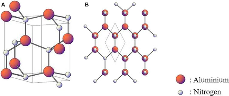
Figure 1. Schematics of (A) 3-D aluminum nitride (AlN) crystal construction and (B) 2-D AlN crystal assembly.
Experimentally, the X-ray diffraction (XRD) data obtained using a Cu-Kα source (wavelength of 0.1540598 nm) X-ray diffractometer were analyzed to explore the crystallinity of sputtered AlN thin films. Figure 2A shows the XRD pattern of sputtered AlN thin films at a plasma power of 300 W and with different back pressures. The main peaks of the sputtered AlN thin films are observed at Bragg's as 33.3°, 36.0°, 37.5°, and 42.6° corresponding to the crystallographic planes (100), (002), (101), and (220), respectively. A comparison of observed and standard ‘d' values of (hkl) planes as matched with Card 01-070-2545 indicates that the AlN thin film is polycrystalline and adopts a wurtzite hexagonal structure [44, 45]. We found that AlN exhibits a polycrystalline structure with a clear (002) orientation. As we increased the back pressure from 0.2 to 0.6 Pa, the (002) peak intensity has increased, indicating a considerable contraction of the corresponding full-width half-maximum (FWHM). More details on the effect of the sputtering conditions on the XRD patterns of textured AlN thin films oriented about the c-axis can be found in Ababneh et al. [24, 25]. The highest peak intensity was found for AlN thin films with (002) orientation. As the back pressure is increased, we observed a considerable increase in the grain size as well as a noticeable improvement of the degree of crystallinity associated with the preferred (002) orientation. Additionally, Figure 2A demonstrates that there is a little shift of all diffraction lines toward the lower diffraction angles (2θ) as the sputtering pressure is increased. The shift in the peaks can be attributed to the sustainable strain in the structure as the sputtering pressure is increased.
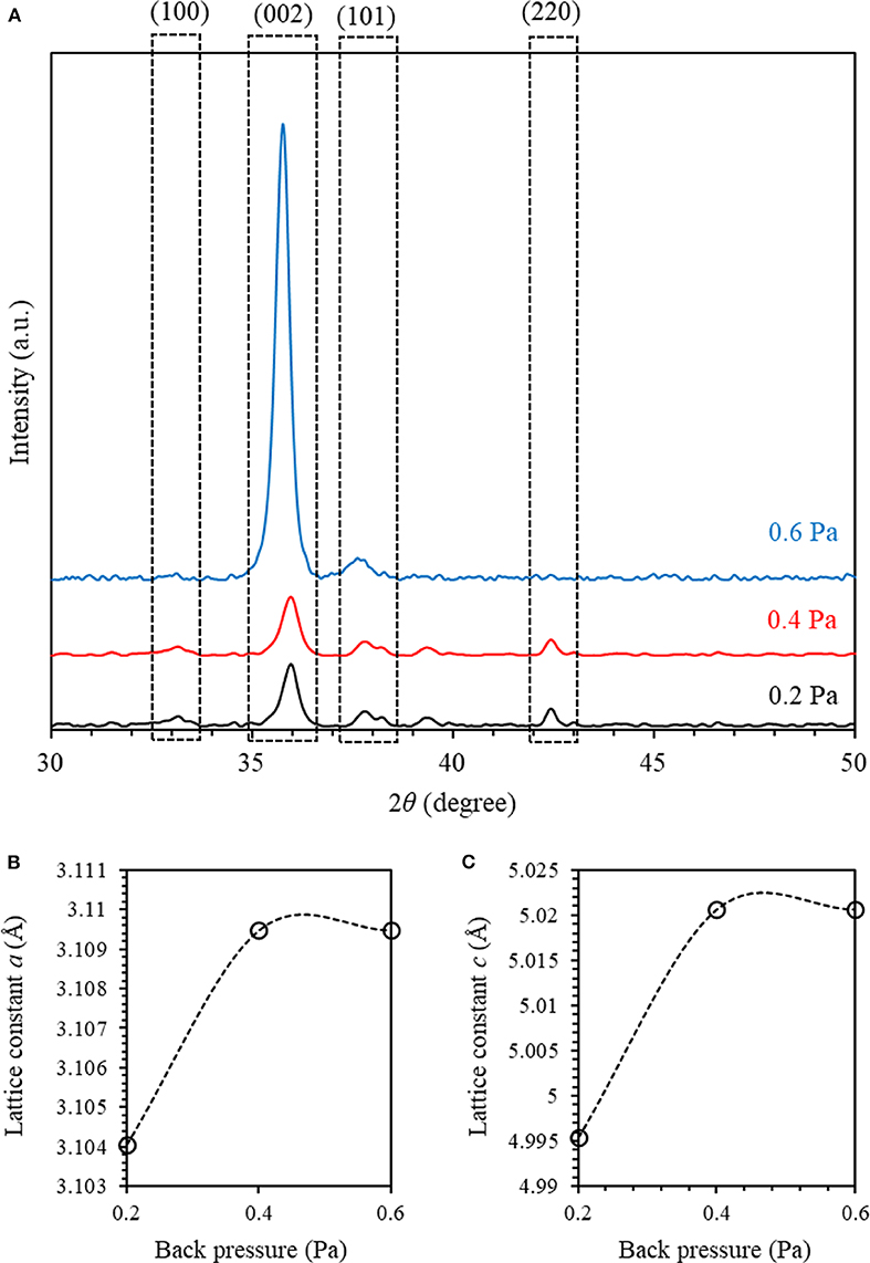
Figure 2. (A) The X-ray diffraction (XRD) configurations of 550-nm thick aluminum nitride (AlN) thin films sputtered on a silicon substrate at a plasma power of 300 W and with different back pressures with 100% N2 atmosphere. (B,C) The in-plane and out-plane lattice constants (a) and (c) obtained from XRD patterns of sputtered AlN thin films as a function of back pressure, respectively.
Our DFT-based simulations show that AlN exhibits a hexagonal structure that belongs to a space group P63mc which has an in-plane lattice constant, a, equal to 3.0977 eV and an out-plane lattice constant c = 4.9668 eV. Moreover, the lattice constants (a) and (c) of the hexagonal structure can be calculated from the relation [46, 47]:
where d(hkl) is the interplanar spacing that can be calculated using Bragg's law and the angle of incidence θ : λ = 2dhkl sin θhkl [48–52]. From Equation (1) and Bragg's law, the lattice constants of the wurtzite microstructure of AlN thin films can be evaluated as:
The obtained values of a and c of the AlN thin film at a back pressure of 0.2 Pa were found to be 3.104 and 4.995 Å, respectively. As the back pressure increases, the a and c slightly increase to 3.109 and 5.021 Å at a back pressure of 0.4 and maintain approximately the same values as the back pressure increases further to 0.6 Pa (as shown in Figures 2B,C). The lattice parameters obtained agree well with the calculated parameters.
The crystalline size, D, can be obtained from Debye Scherrer's formula as D = kλ/β cosθ [46, 53], where D is the crystallite size, β in radians stands for the FWHM, and θ and k represent the Bragg angle and the Scherrer parameter, respectively [54, 55]. Several factors contribute to the lattice microstrain 〈ε〉 such as crystal imperfections, lattice dislocations, and stacking faults [56]. The microstrain of the thin films can be expressed as 〈ε〉 = βcotθ4 [53]. The estimated values of the crystallite size, D, and the average microstrain, 〈ε〉, were plotted as functions of sputtering pressure (as shown in Figure 3). At a back pressure of 0.2 Pa, the crystallite size of the AlN thin film was found to be 17.77 nm. However, increasing the back pressure to 0.4 and 0.6 Pa leads to a considerable increase of the crystallite size to 19.579 and 19.578 nm, respectively. It is obvious that increasing the sputtering back pressure would lead to an increase of the degree of crystallinity and in turn to the increase of the crystallite size. This interplay can be interpreted in terms of the formation of larger atomic groups that would lead to an increase in crystallite size. In addition, Figure 3 indicates that, as the back pressure increases, the microstrain decreases. The opposite trend of the microstrain and the crystallite size could be explained by the fact that, as the volume is occupied by the ordered atoms inside the large atomic crystalline structure, the total surface area increases. This would decrease the shift of plane position and thus reduces the microstrain [57].
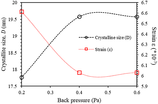
Figure 3. The crystallite size, D, and the microstrain 〈ε〉 of sputtered as-prepared aluminum nitride thin films as a function of back pressure.
A UV–vis spectrophotometer, with a total internal integrating sphere, was employed to investigate the transmittance spectra T%(λ) of sputtered AlN thin films at 300 W and with different back pressures (0.2, 0.4, and 0.6 Pa) in the spectral range of 250–800 nm. Figure 4 shows the transmittance spectra T(λ) of crystalline sputtered as-prepared thin films of AlN. Clearly, the transmittance spectra of the AlN thin films reveal discrete interloping peripheries in the spectral zone of high transparency. This spectral region is characterized by high intensity (~92%). In the short wavelength region, the films begin to absorb the incident light, and consequently the intensity of interloping peripheries begins to decrease and totally vanishes as soon as the absorption edge appears. It was reported that the number of interloping peripheries is basically determined by the thickness of the thin films [58]. The average thin film thickness synthesized has a relatively small value (550 nm); as a result, few observed interloping peripheries are obtained (four fringes only). Furthermore, the appearance of interloping peripheries is an indication of high quality and surface homogeneity of the sputtered AlN thin films. We found that, for wavelength λ <300 nm, the transmittance increases rapidly as the wavelength increases. This could be due to the presence of the absorption edge of the AlN thin films and the glass substrate. As illustrated in Figure 4, as the back pressure is increased, the optical transmittance shifts toward a higher-energy region. Therefore, the optical absorption edge is blue-shifted toward a higher energy. This blue-shift is a direct consequence of several factors, mainly the removal of lingering pressures, the improvement of the crystallinity of the sputtered AlN thin films, and the increase in crystallite size [59, 60]. Furthermore, Figure 4 depicts that, at a back pressure of 0.2 Pa, the transmittance spectrum of the sputtered AlN thin films exhibits the lowest value, indicating that the films exhibit the highest index of refraction. Nevertheless, the transmittance of the sputtered AlN thin films at a back pressure of 0.6 Pa exhibits the highest value, indicating that the films exhibit the lowest refractive index. The inset in Figure 4 presents a typical transmittance spectrum, T(λ), of sputtered AlN thin films at a back pressure of 0.2 Pa. It also shows two envelopes for TM and Tm of sputtered AlN thin films. TM and Tm stand for the experimental maximum and minimum transmittance at a given wavelength, respectively.
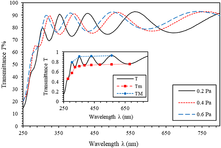
Figure 4. Transmittance spectra of sputtered aluminum nitride (AlN) thin films at 300 W and with different back pressures (0.2, 0.4, and 0.6 Pa). The figure inset shows a typical transmission spectrum of sputtered AlN thin films at a back pressure of 0.2 Pa; TM and Tm are the experimental curves as explained in the text.
Following the derivations of Aly [61], the index of refraction of AlN thin films, n, can be written as Dahshan et al. [62] and Aly et al. [63]:
where and . TM and Tm stand for the maximum and minimum transmittance, respectively. The corresponding index of refraction and transmittance of the glass substrate are denoted by S and Ts, respectively. The film thickness (d) can be given approximately by Aly et al. [63] and Aly [64]:
We found the film thickness to be about 550 nm. Using the values of the refractive index (n) calculated by Swanepoel's method, n(λ) can be expressed in terms of a reasonable two-term function as Aly [64]:
where a and b are the least square fitted constants. Equation (6) shows that by plugging the values of a and b therein, n(λ) can be determined over the entire spectrum (250–800 nm) [65]. As illustrated in Figure 5, the refractive index, n, decreases slowly as the wavelength is increased, and it drops significantly as the back pressure is increased.
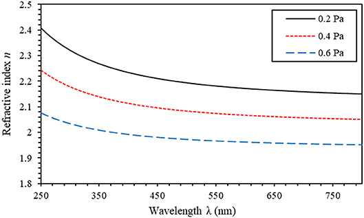
Figure 5. Refractive index of sputtered aluminum nitride thin films at 300 W and with different back pressures (0.2, 0.4, and 0.6 Pa) with 100% N2 atmosphere.
Tauc plot is commonly used to estimate the band gap energy of semiconductors. It is defined by relating the absorption coefficient with the incident photon energy (hv) as [66], where the parameter β indicates band tailing, Eg stands for optical band gap, and the number n labels the transition type [67]. The value (n) of crystalline AlN thin films is 1/2 corresponding to the direct allowed transition. Tauc plot has been used by drawing the relationship between the incident energy of the photon (hυ) in eV vs. (αhυ)2. Figure 6 shows the Tauc plot of sputtered AlN thin films at 300 W and with different back pressures (0.2, 0.4, and 0.6Pa). The band gap of the AlN thin film at 0.2 Pa was found to be 4.51 eV. As sputtering pressure is increased to 0.004 and 0.006 mbar, the band gap energy was found to increase to 4.46 and 4.54 eV, respectively. The reported value of the band gap of AlN is 6.11 eV. The difference between the calculated and the reported values is due to the band gap of the glass substrate.
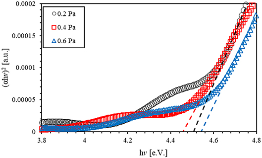
Figure 6. Tauc optical band gap energy of sputtered aluminum nitride thin films at 300 W and with different back pressures (0.2, 0.4, and 0.6 Pa).
In order to calculate the electronic band structure of AlN, we employed GGA and hybrid functional HSE06 [68] for exchange correlation potential. Figure 7A depicts the electronic band structure of the AlN thin films. Our results indicate that the AlN thin films exhibit a direct band gap at Γ point, consistent with that of bulk AlN. It is expected that the calculated optical band gap is smaller than the measured value as it is customary for DFT-based ab initio electronic simulations to underestimate the value of the optical band gap of metals and semiconductors. One thing to note here is that the first-principle DFT based on GGA suffers from the inevitable gap underestimate [69–71], and this problem may affect the correctness of the calculated band gaps. Therefore, a hybrid functional [68] that evaluates the Fock exchange in real space was introduced. We used the hybrid functional HSE06 to calculate the electronic and the optical properties of AlN. It is expected that the optical band gap obtained using the HSE06 hybrid functional method is more accurate than the one predicted by the GGA method. The band gap energy estimated using the GGA method was found to be 3.72 eV, while the band gap energy estimated using the HSE06 hybrid functional method was found to be 5.07 eV. It can thus be concluded that the calculated values of the band gap energy using HSE06 are more accurate than the values calculated using the GGA method [72–74]. This difference could be due to the vacancy's formation during synthesis and the difference between the experimental and the calculated chemical potentials of the constituents. The electronic properties of AlN can be obtained by executing self-consistent electronic ab initio simulations. In particular, electronic density of states (DOS), partial density of states (PDOS), and the electronic band structure are calculated self-consistently [75]. Figures 7B,C display the DOS and the PDOS of AlN thin films using (GGA) and hybrid functional HSE06, respectively. Our results indicate that the bonding between the Al and the N atoms is ionic. Obviously, Figures 7B,C show that there is an expurgated in DOS plot past the Fermi level which designates the optical band gap. The peaks at 3 eV directly above the Fermi level belong to the N electronic state of the conduction band. The DOS and PDOS plots indicate that the states dominating the valence band maximum have energies of−4.62,−4.25,−3.53,−2.33,−1.13, and−0.72 eV below the Fermi level.
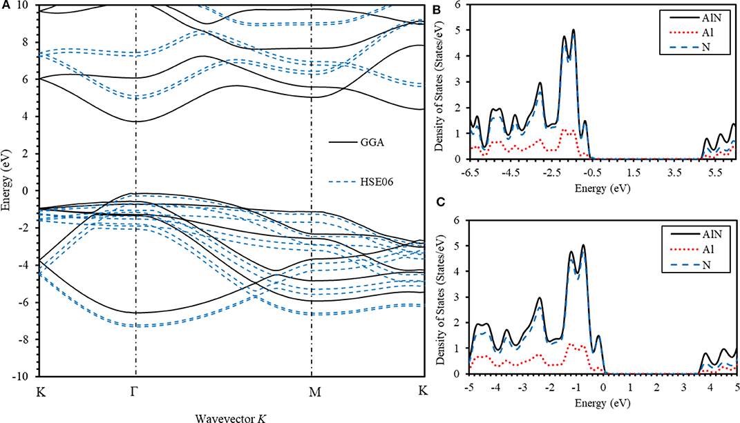
Figure 7. (A) The calculated electronic band structure of aluminum nitride (AlN) system using GGA and HSE06 methods. (B) Total DOS and PDOS of AlN, Al, and N atoms using GGA method and (C) total DOS and PDOS of AlN, Al, and N atoms using HSE06 method.
Dispersion parameters such as the effective single oscillator (E0), dispersion energy (Ed), and static dielectric constant (ε0) were determined using the Wemple–DiDomenico single effective-oscillator model [53, 76, 77] expressed as:
By plotting (n2 − 1)−1 vs. (hv)2, the dispersion parameters can be evaluated by fitting a straight line. The values of E0 and Ed can then be calculated from the slope . The values of the dispersion parameters Ed and E0 of the AlN thin films for different values of back pressure are reported in Table 1. Clearly, the E0 value of the AlN thin films increases as the plasma power is increased. The increase of the E0 values of the AlN thin films could be explained as follows: As the plasma power increases, the energy of the bonds between the constituent atoms of the thin film increases, leading to an increase in the values of E0, indicating the sensitivity of this parameter to the bond energy as predicted previously [78]. The obtained values of E0 and Ed are closely related to the ε0 and the static index of refraction n0 as can be deduced from Equation (7) by putting hv = 0,
The calculated values of ε0 and n0 of the AlN thin films are presented in Table 1. We found that the values of n0 agree well with the available theoretical and experimental values of the normal index of refraction. The ε0 and the n0 values of the AlN thin film at 0.5 Pa are found to be 4.54 and 2.13, respectively. We found that, as the back pressure increases to 0.4 and 0.6 Pa, the ε0 decreases to 4.14 and 3.77, respectively. An accurate measurement of the refractive index is essential to get the free carriers to the effective mass ratio (N/m*) and the frequency-dependent dielectric constant ε∞ as comprehended by Fasasi et al. [79] and Spitzer and Fan [80]:
where e is the value of the electronic charge, Nc represents the charge carrier density, m* is the effective mass of the carrier, and ε∞ is the high-frequency dielectric constant. Plotting n2 vs. λ2 yields a straight line in the long-wavelength region. The density of states N/m* is determined from the slope of the straight line. The ε∞ parameter can be obtained by extrapolating the straight line to λ2 = 0. The values obtained are presented in Table 1. The value of ε∞ of the AlN thin film at 0.2 Pa is found to be 4.938. As the back pressure increases, ε∞ decreases. Our results provide substantial evidence that the free charge carriers of AlN thin films strongly contribute to their polarization [81, 82].
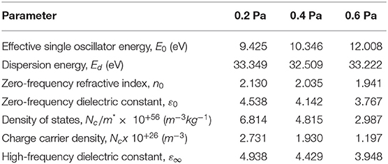
Table 1. Estimation of some essential optical parameters of aluminum nitride thin films sputtered at different back pressures.
The dielectric properties of AlN were investigated by calculating their response to homogeneous electric fields. We used the density functional perturbation theory [83, 84] to measure the dielectric constants of the thin films. The density functional perturbation theory has been able to precisely investigate the electric field response of the isolated crystal. The static dielectric tensor calculation involves the computation of the electronic and the elastic-piezoelectric response to an external electric field. The static dielectric tensor elements are:
where E and P stand for the electric field and the total macroscopic polarization. The static dielectric tensor and the susceptibility tensor χij defined at vanishing strain are related via . The static dielectric tensor can be decomposed into electronic contribution and lattice contribution. We calculated the diagonal components of of the AlN crystal under the effect of an external field as presented in Table 2. We found a good agreement between the calculated values of the static dielectric tensor and the experimental values of the zero-frequency dielectric constant measured at 0.2 and 0.4 Pa as can be clearly seen from Table 1. At a higher back pressure of 0.6 Pa, we found that the calculated diagonal elements of static deviate from the experimental zero-frequency dielectric constant as expected. Our results indicate that, as the back pressure is increased, the discrepancy between the calculated and the experimental becomes obvious. An accurate calculation of the dielectric constant is fundamental for parameterization of scaled devices. The proper functioning of such scaled devices depends considerably on an appropriate description of the long-wave lattice dynamics [84].

Table 2. The electronic contribution to the static dielectric tensor of aluminum nitride including local field effects (applying external electric field).
Investigating the lattice dynamics of the AlN crystal requires an accurate calculation of Born effective charge tensor . The piezoelectric response of the AlN crystal is mainly determined from the interplay of structural fluctuations and the components of tensor of the Al and the N ions. We calculated the tensors of AlN crystal using the density functional perturbation theory and by applying the electric field Ej. Accordingly, can be expressed as Alsaad et al. [84]:
where ∂Pj is the polarization induced by the periodic displacement ∂ui, k or to the force Fi, k induced on atom i by the electric field Ej. In addition, tensor couples the macroscopic polarization Pj and periodic atomic displacements via:
where i denotes the ith atom and j and k are the directions of the polarization component and the atomic displacement, respectively. The tensor of the Al and the N ions of the AlN crystal was calculated from the response to a homogenous electric field. Our results are in good agreement with the previous results [85, 86].
Table 3 indicates that the acoustic-sum rule [87] that examines the charge neutrality is satisfied. For every direction i and j, one must have [88]. As can be seen from Table 3, the of the Al atoms covalently bonded to the nitrogen atom is positive and effectively creates a local dipole moment with the negatively charged nitrogen atoms.
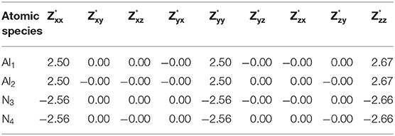
Table 3. Calculated Born effective charge tensor of aluminum and nitrogen ions of aluminum nitride calculated by applying a homogenous electric field = + 0.02ŷ + 0.02ẑ eV/Å.
Wurtzite piezoelectric materials have about two orders of magnitude lesser piezo-response compared to Perovskite materials. However, materials like wurtzite AlN can maintain a hysteresis-free behavior, with high-temperature thermal stability and easier production techniques. The piezoelectric stress coefficient (eijk) can be expressed as Duerloo et al. [89]:
The piezoelectric coefficient can be decomposed into a clamped-ion part () and an internal-strain part (), i.e., [90, 91]. In principle, the clamped-ion piezoelectric coefficient can be defined as Alsaad et al. [84]:
In terms of energy per undeformed unit volume, the clamped-ion piezoelectric tensors can be written as:
and the internal-strain piezoelectric coefficient as:
In Table 4 is a list of the calculated clamped-ion piezoelectric coefficient tensor for wurtzite AlN. The coefficients and which represent the induced polarization produced along the z-axis per unit stress applied along the z-axis and the x-axis, respectively, exhibit the largest values, indicating a large piezoelectric response. Therefore, it is interesting to get advantage of this large piezoelectric response for the purpose of designing AlN-based piezoelectric devices. Our results are in good agreement with previously reported results [92, 93].
In addition, the significant values of and show considerable rotation and twisting of the electric dipole about the z-direction as uniaxial strain η33 and shear strain η31 are applied. The uniaxial strain η33 twists the Al–N bond, causing the polarization vector to rotate along the z-direction, producing a large change in the electric dipole as clearly demonstrated in Figures 8A–C that show the 3D and the 2D plots of the piezoelectric tensor of AlN. Figure 8D shows the default plot of the magnitude, indicating along which direction the polarization is the largest.
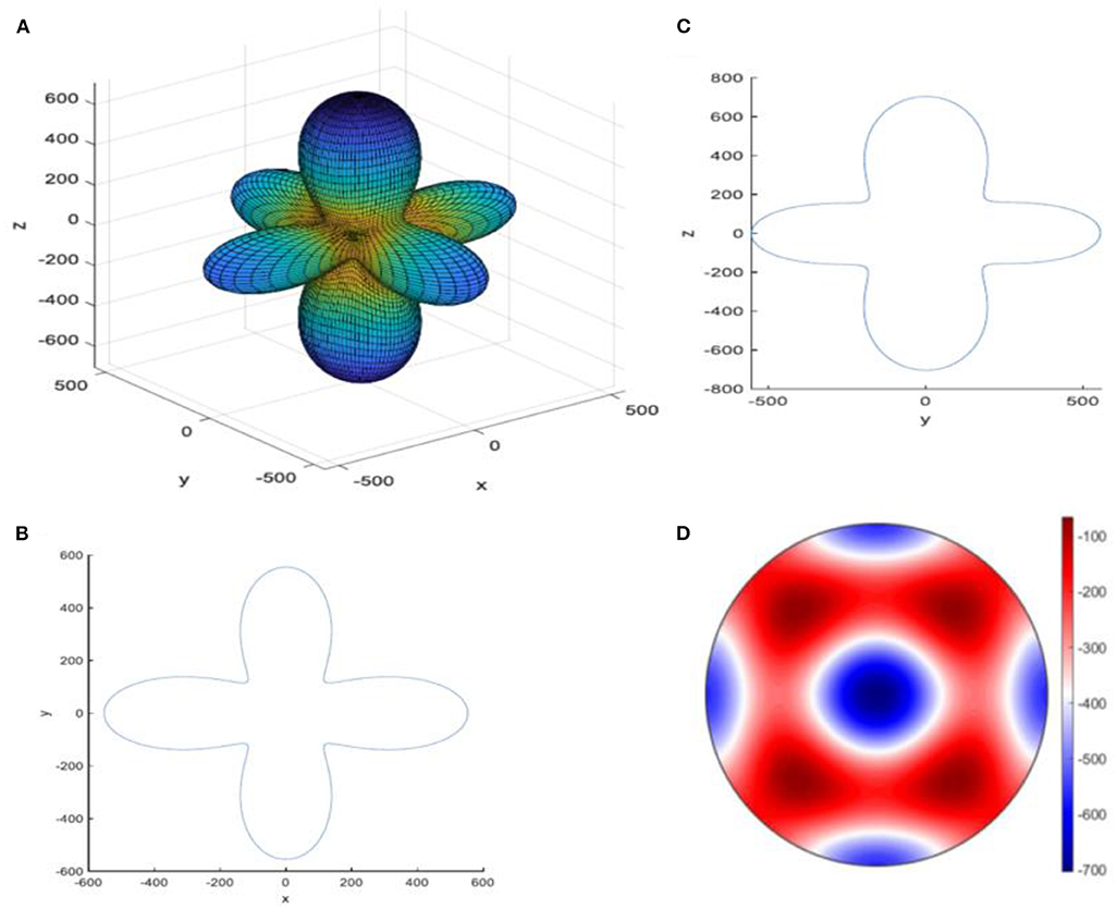
Figure 8. (A) 3D plot, (B) xy 2D plot, (C) yz 2D plot, and (D) the magnitude of the largest value of the piezoelectric tensor of aluminum nitride crystal.
It is customary to define the force–response internal strain tensor as Alsaad et al. [84]:
Usually, crystals with basis contain one or more atoms that subjugate sites lacking inversion symmetry and which exhibit considerable internal strain tensors. Table 5 shows the internal strain tensor of the displaced atoms of Al and N atoms. The computation of internal strain tensors is crucial for the determination of the different inner elastic constants of the AlN crystal. Thus, theoretically, they provide a deeper insight into understanding the structure and bonding. Practically, they are essential for tracking atomic displacements in a homogeneously stressed crystal and consequently are relevant to the elucidation of the properties of crystals that are explored under conditions of precisely defined stress.
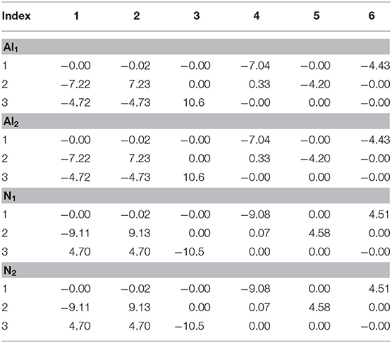
Table 5. Internal strain tensor (Voigt notation) of Al1, Al2, N1, and N2 for displacements in x, y, and z (eV/Å).
A deep understanding of the elastic properties of AlN could be useful for potential applications of AlN in flexible electronic devices. The elastic stiffness of AlN has a symmetric form. It is an inherited feature of the space group P63mc to which AlN belongs. The calculated elements of the elastic moduli are presented in Table 6. Figures 9A–C show the two- and three-dimensional surface constructions of the elastic modulus of AlN. It is obvious that the elastic modulus of AlN exhibits an apparent deviation in shape from spherical symmetry, indicating a strong anisotropic behavior along different symmetrical directions. The 3D contour deviates from the spherical shape laterally along the z-axis, along which it exhibits the largest value. The large deviation from the spherical shape along the z-axis indicates that the elastic modulus of AlN is highly anisotropic. Figure 9D shows the default plot of the magnitude of the elastic constant, indicating that AlN exhibits the maximum value along the z-direction.
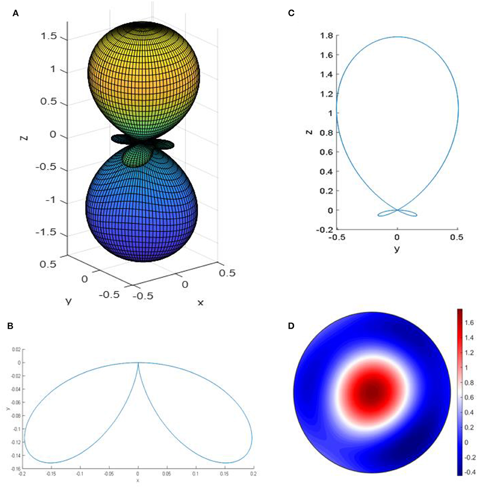
Figure 9. (A) 3D plot, (B) xy 2D plot, (C) yz 2D plot, and (D) the magnitude of the largest value of the elastic modulus of aluminum nitride.
We parameterized the elastic stiffness tensor of AlN. We found it to be symmetrical λij = λji as illustrated in Table 6, confirming that the elastic tensor is isotropic. The table shows that AlN exhibits negative diagonal elastic moduli, and the magnitudes of the components indicate that the material is relatively soft. This result shows that this material has a potential to be used in flex circuits for flexible electronic applications [94]. A sophisticated electronic skin that senses pressure pulses demonstrated on an integrated display of organic light-emitting diodes has been reported [95–104]. We found that AlN exhibits Young's modulus of 302 GPa and shear modulus of 126 GPa, along with its light weight and non-toxic nature, making it eligible as a substrate for flex circuit boards and electronic skin.
In summary, piezoelectric aluminum nitride thin films were synthesized by reactive DC-magnetron sputtering on a glass substrate with different back pressures. The optimization process was performed to obtain highly textured thin films with enhanced piezoelectric response via studying the interplay between the microstructure and the electronic, optical, piezoelectric, and dielectric properties. X-ray powder diffraction was used to investigate the structural properties. The XRD measurements confirm that the AlN thin films exhibit a hexagonal structure. The dominant crystallographic orientation is found to be (002) plane with the optimum intensity in comparison with other possible orientations. VASP based on density functional theory and generalized gradient approximation was used to investigate the structural and the electronic properties of hexagonal AlN structures. The experimental and the theoretical optimized lattice parameters of AlN were found to be in good agreement. The optical properties of sputtered AlN thin films at different back pressures were investigated by performing UV–vis spectrophotometer measurements of their transmittance spectra. The refractive index and the optical band gap of the sputtered AlN thin films were calculated accordingly. The refractive index of the AlN thin films was found to be 2.15. We found that the measured optical band gap of the AlN thin film (4.5 eV) is higher than the ab initio calculated value that is found to be 3.85 eV, consistent with the previously reported calculated value. This discrepancy is expected as it is well known that first-principle techniques underestimate the optical band gap considerably. In addition, the elastic, piezoelectric, and dielectric tensors of AlN crystal were calculated by employing VASP within the framework of DFT. The dynamical Born effective charge tensor of the AlN system that is crucial for lattice dynamical investigations was reported for all atoms in the unit cell. The value of the principal component of electronic contribution to the static dielectric tensor of AlN was found to be ≈4.68. Furthermore, clamped-ion piezoelectric tensor was calculated. The diagonal components were found to be e33 = 1.784 and , demonstrating a reasonable piezoelectric response of this polar crystal. The interplay between the structural, electronic, optical, elastic, and piezoelectric properties of the polar AlN crystal indicates a potential attractive perspective for cheap and efficient optoelectronic, piezoelectric, and mechanical applications. Based on our results, AlN films are promising for communication systems, electromechanical, dielectric, and piezoelectric applications, and information storage devices.
The datasets generated for this study are available on request to the corresponding author.
AMA, QA-B, IQ, AAA, AA, ZA, IA, and AT: measurements of physical tensors and elastic properties, data analysis and acquisition, and editing the manuscript.
The authors declare that the research was conducted in the absence of any commercial or financial relationships that could be construed as a potential conflict of interest.
The authors would like to thank Jordan University of Science and Technology for the financial and the technical support provided by the deanship of scientific research. The second author would like to acknowledge the technical support provided by Holland Computing Centre affiliated to University of Nebraska at Omaha (UNO), United States. We would like to acknowledge the support of Khalifa University of Science and Technology, Abu Dhabi, United Arab Emirates.
1. Wang C, Chiu M, Shiao M, Shieu F. Characterization of AlN thin films prepared by unbalanced magnetron sputtering. J Electrochem Soc. (2004) 151:F252–6. doi: 10.1149/1.1790531
2. Akiyama M, Morofuji Y, Kamohara T, Nishikubo K, Tsubai M, Fukuda O, et al. Flexible piezoelectric pressure sensors using oriented aluminum nitride thin films prepared on polyethylene terephthalate films. J Appl Phy. (2006) 100:114318. doi: 10.1063/1.2401312
3. Marzencki M, Ammar Y, Basrour S. Integrated power harvesting system including a MEMS generator and a power management circuit. Sens Actuat A. (2008) 145:363–70. doi: 10.1016/j.sna.2007.10.073
4. Ingrosso I, Petroni S, Altamura D, De Vittorio M, Combi C, Passaseo A. Fabrication of AlN/Si SAW delay lines with very low RF signal noise. Microelectronic Eng. (2007) 84:1320–4. doi: 10.1016/j.mee.2007.01.100
5. Matsunami N, Kakiuchida H, Sataka M, Okayasu S. XRD characterization of AlN thin films prepared by reactive RF-sputter deposition. Adv Mater Phy Chem. (2013) 3:101. doi: 10.4236/ampc.2013.31A012
6. Akiyama M, Kamohara T, Ueno N, Sakamoto M, Kano K, Teshigahara A, et al. Polarity inversion in aluminum nitride thin films under high sputtering power. Appl Phy Lett. (2007) 90:151910. doi: 10.1063/1.2721865
7. Olivares J, González-Castilla S, Clement M, Sanz-Hervás A, Vergara L, Sangrador J, et al. Combined assessment of piezoelectric AlN films using X-ray diffraction, infrared absorption and atomic force microscopy. Diamond Related Mater. (2007) 16:1421–4. doi: 10.1016/j.diamond.2006.11.065
8. Adam T, Kolodzey J, Swann C, Tsao M, Rabolt J. The electrical properties of MIS capacitors with AlN gate dielectrics. Appl Surface Sci. (2001) 175:428–35. doi: 10.1016/S0169-4332(01)00091-5
9. Liufu D, Kao K. Piezoelectric, dielectric, interfacial properties of aluminum nitride films. J Vacuum Sci Technol A. (1998) 16:2360–6. doi: 10.1116/1.581352
10. Cheng CC, Chen YC, Wang HJ, Chen WR. Low-temperature growth of aluminum nitride thin films on silicon by reactive radio frequency magnetron sputtering. J Vacuum Sci Technol A. (1996) 14:2238–42. doi: 10.1116/1.580053
11. Gudovskikh A, Alvarez J, Kleider J-P, Afanasjev V, Luchinin V, Sazanov A, et al. Polycrystalline AlN films deposited at low temperature for selective UV detectors. Sensors Actuat A. (2004) 113:355–9. doi: 10.1016/j.sna.2004.02.017
12. Tsubouchi K, Mikoshiba N. Zero-temperature-coefficient SAW devices on AlN epitaxial films. IEEE Trans Sonics Ultrasonics. (1985) 32:634–44. doi: 10.1109/T-SU.1985.31647
13. Chen Q, Qin L, Wang Q-M. Property characterization of AlN thin films in composite resonator structure. J Appl Phy. (2007) 101:084103. doi: 10.1063/1.2716391
14. Hong H.S, Chung G-S. E ect of thermal annealing on the SAW properties of AlN films deposited on Si substrate. J Korean Phy Soc. (2009) 54. doi: 10.3938/jkps.54.1519
15. Dimitrova V, Manova D, Valcheva E. Optical dielectric properties of dc magnetron sputtered AlN thin films correlated with deposition conditions. Mater Sci Eng B. (1999) 68:1–4. doi: 10.1016/S0921-5107(99)00221-4
16. Schupp T, Lischka K, As D. MBE growth of atomically smooth non-polar cubic AlN. J Cryst Growth. (2010) 312:1500–4. doi: 10.1016/j.jcrysgro.2010.01.040
17. Vispute R, Wu H, Narayan J. High quality epitaxial aluminum nitride layers on sapphire by pulsed laser deposition. Appl Phy Lett. (1995) 67:1549–51. doi: 10.1063/1.114489
18. Cheng H, Sun Y, Zhang J, Zhang Y, Yuan S, Hing P. AlN films deposited under various nitrogen concentrations by RF reactive sputtering. J Cryst Growth. (2003) 254:46–54. doi: 10.1016/S0022-0248(03)01176-X
19. Venkataraj S, Severin D, Drese R, Koerfer F, Wuttig M. Structural, optical and mechanical properties of aluminium nitride films prepared by reactive DC magnetron sputtering. Thin Solid Films. (2006) 502:235–9. doi: 10.1016/j.tsf.2005.07.281
20. Takikawa H, Kimura K, Miyano R, Sakakibara T, Bendavid A, Martin PJ, et al. Effect of substrate bias on AlN thin film preparation in shielded reactive vacuum arc deposition. Thin Solid Films. (2001) 386:276–80. doi: 10.1016/S0040-6090(00)01673-4
21. Chen H-Y, Han S, Shih HC. The characterization of aluminum nitride thin films prepared by dual ion beam sputtering. Surf Coat Technol. (2006) 200:3326–9. doi: 10.1016/j.surfcoat.2005.07.046
22. Thapa R, Saha B, Chattopadhyay K. Synthesis of cubic aluminum nitride by VLS technique using gold chloride as a catalyst and its optical and field emission properties. J Alloys Compounds. (2009) 475:373–7. doi: 10.1016/j.jallcom.2008.07.020
23. Fahana MAN, Lee ZY, Fong CY, Ng SS. Growth characterization of AlN thin film deposited by sol-gel spin coating techniques. Adv Mater Res. (2015) 1107:667–71. doi: 10.4028/www.scientific.net/AMR.1107.667
24. Ababneh A, Schmid U, Hernando J, Sánchez-Rojas J, Seidel H. The influence of sputter deposition parameters on piezoelectric and mechanical properties of AlN thin films. Mater Sci Eng B. (2010) 172:253–8. doi: 10.1016/j.mseb.2010.05.026
25. Ababneh A, Albataineh Z, Dagamseh A, kofahi-Al I, Schäfer B, Zengerle T, et al. Optical characterization of sputtered aluminum nitride thin films-correlating refractive index with degree of c-axis orientation. Thin Solid Films. (2020) 693:137701. doi: 10.1016/j.tsf.2019.137701
26. Hohenberg P, Kohn W. Inhomogeneous electron gas. Phys Rev. (1964) 136:B864. doi: 10.1103/PhysRev.136.B864
27. Kohn W, Sham LJ. Self-consistent equations including exchange and correlation effects. Phys Rev. (1965) 140:A1133. doi: 10.1103/PhysRev.140.A1133
28. Heyd J, Scuseria GE, Ernzerhof M. Hybrid functionals based on a screened Coulomb potential. J Chem Phy. (2003) 118:8207–15. doi: 10.1063/1.1564060
29. Heyd J, Scuseria GE. Efficient hybrid density functional calculations in solids: assessment of the Heyd-Scuseria-Ernzerhof screened Coulomb hybrid functional. J Chem Phy. (2004) 121:1187–92. doi: 10.1063/1.1760074
30. Batista ER, Heyd J, Hennig RG, Uberuaga BP, Martin RL, Scuseria GE, et al. Comparison of screened hybrid density functional theory to diffusion Monte Carlo in calculations of total energies of silicon phases and defects. Phy Rev B. (2006) 74:121102. doi: 10.1103/PhysRevB.74.121102
31. Kresse G. Kresse G, Joubert D. From ultrasoft pseudopotentials to the projector augmented-wave method. Phys Rev B. (1999) 59:1758–75. doi: 10.1103/PhysRevB.59.1758
32. Adolph B, Furthmüller J, Bechstedt F. Optical properties of semiconductors using projector-augmented waves. Phy Rev B. (2001) 63:125108. doi: 10.1103/PhysRevB.63.125108
33. Blöchl PE. Projector augmented-wave method. Phy Rev B. (1994) 50:17953. doi: 10.1103/PhysRevB.50.17953
34. Kresse G, Hafner J. Ab initio molecular-dynamics simulation of the liquid-metal-amorphous-semiconductor transition in germanium. Phy Rev B. (1994) 49:14251–69. doi: 10.1103/PhysRevB.49.14251
35. Bates S, Kresse G, Gillan M. A systematic study of the surface energetics and structure of TiO2 (110) by first-principles calculations. Surf Sci. (1997) 385:386–94. doi: 10.1016/S0039-6028(97)00265-3
36. Kresse G. Kresse G, Furthmüller J. Efficient iterative schemes for ab initio total-energy calculations using a plane-wave basis set. Phys Rev B. (1996) 54:11169–86. doi: 10.1103/PhysRevB.54.11169
37. Strak P, Sakowski K, Kempisty P, Grzegory I, Krukowski S. Catalytic synthesis of nitric monoxide at the AlN (0001) surface: ab initio analysis. J Phy Chem C. (2019) 123:10893–906. doi: 10.1021/acs.jpcc.8b12472
38. Koutná N, Rehák P, Chen Z, Bartosik M, Fallmann M, Cerný M, et al. Correlating structural and mechanical properties of AlN/TiN superlattice films. Scripta Materialia. (2019) 165:159–63. doi: 10.1016/j.scriptamat.2019.02.021
39. Kumar A, Prasad M, Janyani V, Yadav R. Optical characterization of RF sputtered AlN thin film for acoustic and optoelectronics devices. In: 2019 9th Annual Information Technology, Electromechanical Engineering and Microelectronics Conference (IEMECON). Jaipur (2019). p. 60–3. doi: 10.1109/IEMECONX.2019.8877067
40. Poudyal A, Jackson N. Characterization of confocal sputtered molybdenum thin films for aluminum nitride growth. Thin Solid Films. (2020) 693:137657. doi: 10.1016/j.tsf.2019.137657
41. French M, Becker A, Lorenzen W, Nettelmann N, Bethkenhagen M, Wicht J, et al. Ab initio simulations for material properties along the Jupiter adiabat. Astrophy J. (2012) 202:5. doi: 10.1088/0067-0049/202/1/5
42. Lim SH, Lin J. Ab initio study of the hydrogen chemisorption of single-walled aluminum nitride nanotubes. Chem Phy Lett. (2008) 466:197–204. doi: 10.1016/j.cplett.2008.10.059
43. Sangiovanni DG, Gueorguiev G, Georgieva-Kakanakova A. Ab initio molecular dynamics of atomic-scale surface reactions: Insights into metal organic chemical vapor deposition of AlN on graphene. Phy Chem Chem Phy. (2018) 20:17751–61. doi: 10.1039/C8CP02786B
44. Park M-H, Kim S-H. Thermal conductivity of AlN thin films deposited by RF magnetron sputtering. Mater Sci Semiconduct Process. (2012) 15:6–10. doi: 10.1016/j.mssp.2011.04.007
45. Khan S, Shahid M, Mahmood A, Shah A, Ahmed I, Mehmood M, et al. Texture of the nano-crystalline AlN thin films and the growth conditions in DC magnetron sputtering. Prog Natl Sci Mater Int. (2015) 25:282–90. doi: 10.1016/j.pnsc.2015.08.006
46. Zak AK, Majid WA, Abrishami ME, Yousefi R. X-ray analysis of ZnO nanoparticles by Williamson-Hall and size-strain plot methods. Solid State Sci. (2011) 13:251–6. doi: 10.1016/j.solidstatesciences.2010.11.024
47. Cullity BD. Elements of X-Ray Diffraction. Wellesley, MA: Addison-Wesley Publishing Company, Inc. (1978).
48. Ahmad A, Alsaad A, Al-Bataineh Q, Salameh-Bani A, Al-Khateeb H, Al-Naafa M. Optical structural characterization of dip synthesized Al-B Co-doped ZnO seeded platforms for ZnO nanostructures. J Phy. (2017) 2017:33–48. doi: 10.1007/s00339-018-1875-z
49. Bussi Y, Golan S, Dosoretz CG, Eisen MS. Synthesis, characterization and performance of polystyrene/PMMA blend membranes for potential water treatment. Desalination. (2018) 431:35–46. doi: 10.1016/j.desal.2017.12.024
50. Lu H, Li T, Poddar S, Goit O, Lipatov A, Sinitskii A, et al. Statics and dynamics of ferroelectric domains in diisopropylammonium bromide. Adv Mater. (2015) 27:7832–38. doi: 10.1002/adma.201504019
51. Gao K, Xu C, Cui Z, Liu C, Gao L, Li C, et al. The growth mechanism and ferroelectric domains of diisopropylammonium bromide films synthesized via 12-crown-4 addition at room temperature. Phys Chem Chem Phys. (2016) 18:7626–31. doi: 10.1039/C6CP00568C
52. Mulla S, Phale P, Saraf M. Use of ray diffraction technique for polymer characterization and studying the effect of optical accesories. In: AdMet Paper NOM. Vol. 6. London: ARAI (2012).
53. Fu DW, Zhang W, Cai HL, Ge JZ, Zhang Y, Xiong RG. Diisopropylammonium chloride: a ferroelectric organic salt with a high phase transition temperature and practical utilization level of spontaneous polarization. Adv Mater. (2011) 23:5658–62. doi: 10.1002/adma.201102938
54. Shull C. The determination of X-ray diffraction line widths. Phys Rev. (1946) 70:679. doi: 10.1103/PhysRev.70.679
55. Pielaszek R. Diffraction studies of microstructure of nanocrystals exposed to high pressure (Ph. D. thesis). Department of Physics, Warsaw University, Warsaw, Poland (2003).
56. Zhang J-M, Zhang Y, Xu K-W, Ji V. General compliance transformation relation and applications for anisotropic hexagonal metals. Solid State Commun. (2006) 139:87–91. doi: 10.1016/j.ssc.2006.05.026
57. Horiuchi S, Tokunaga Y, Giovannetti G, Picozzi S, Itoh H, Shimano R, et al. Above-room-temperature ferroelectricity in a single-component molecular crystal. Nature. (2010) 463:789–92. doi: 10.1038/nature08731
58. Ismail-Emam M, El-Hagary M, Shaaban E, Al-Hedeib A. Microstructure optical studies of electron beam evaporated ZnSe1–xTex nanocrystalline thin films. J Alloys Compounds. (2012) 532:16–24. doi: 10.1016/j.jallcom.2012.04.013
59. Ashraf M, Akhtar S, Khan A, Ali Z, Qayyum A. Effect of annealing on structural and optoelectronic properties of nanostructured ZnSe thin films. J Alloys Compounds. (2011) 509:2414–9. doi: 10.1016/j.jallcom.2010.11.032
60. Hassanien A, Aly K, Akl AA. Study of optical properties of thermally evaporated ZnSe thin films annealed at different pulsed laser powers. J Alloys Compounds. (2016) 685:733–42. doi: 10.1016/j.jallcom.2016.06.180
61. Manifacier J, Gasiot J, Fillard J. A simple method for the determination of the optical constants n, k and the thickness of a weakly absorbing thin film. J Phys E Sci Instr. (1976) 9:1002. doi: 10.1088/0022-3735/9/11/032
62. Dahshan A, Amer H, Aly K. Compositional dependence of the optical constants of amorphous GexAs20Se80– x thin films. J Phys D Appl Phys. (2008) 41:215401. doi: 10.1088/0022-3727/41/21/215401
63. Aly K, Amer H, Dahshan A. Optical constants of thermally evaporated Se-Sb-Te films using only their transmission spectra. Mater Chem Phys. (2009) 113:690–5. doi: 10.1016/j.matchemphys.2008.08.035
64. Aly KA. Optical band gap and refractive index dispersion parameters of As x Se 70 Te 30– x (0 ≤ x ≤ 30 at.%) amorphous films. Appl Phys A. (2010) 99:913–9. doi: 10.1007/s00339-010-5680-6
65. Swanepoel R. Determination of the thickness and optical constants of amorphous silicon. J Phys E Sci Instr. (1983) 16:1214. doi: 10.1088/0022-3735/16/12/023
67. Bhattacharyya D, Chaudhuri S, Pal Bandgap A optical transitions in thin films from reflectance measurements. Vacuum. (1992) 43:313–6. doi: 10.1016/0042-207X(92)90163-Q
68. Heyd J, Scuseria GAssessment E validation of a screened Coulomb hybrid density functional. J Chem phys. (2004) 120:7274–80. doi: 10.1063/1.1668634
69. Al-Bataineh QM, Alsaad A, Ahmad A, Al-Sawalmih A. Structural, electronic and optical characterization of ZnO thin film-seeded platforms for ZnO nanostructures: Sol-Gel method versus Ab initio calculations. J Electr Mater. (2019) 48:5028–38. doi: 10.1007/s11664-019-07303-6
70. Qin G, Wang X, Zheng J, Kong C, Zeng B. First-principles investigation of the electronic and magnetic properties of ZnO nanosheet with intrinsic defects. Comput Mater Sci. (2014) 81:259–63. doi: 10.1016/j.commatsci.2013.08.018
71. Li K, Yan Y, Wang H, Zhan Q, Mohammed YS, Jin H. Ferromagnetism in phosphorus-doped ZnO: first-principles calculation. Phys Lett A. (2010) 374:628–31. doi: 10.1016/j.physleta.2009.11.034
72. Jonnard P, Capron N, Semond F, Massies J, Guerrero-Martinez E, Mariette H. Electronic structure of wurtzite and zinc-blende AlN. Eur Phys J B. (2004) 42:351–9. doi: 10.1140/epjb/e2004-00390-7
73. Litimein F, Bouhafs B, Dridi Z, Ruterana P. The electronic structure of wurtzite and zincblende AlN: an Ab initio comparative study. N J Phys. (2002) 4:64. doi: 10.1088/1367-2630/4/1/364
74. Araujo RB, De Almeida J, Ferreira Da Silva A. Electronic properties of III-nitride semiconductors: a first-principles investigation using the Tran-Blaha modified Becke-Johnson potential. J Appl Phys. (2013) 114:183702. doi: 10.1063/1.4829674
75. Tsegaye ZA. Density functional theory studies of electronic and optical properties of ZnS alloyed with Mn and Cr. Bergen: Institutt for fysikk (2012).
76. Sutcliffe BT, Wilson S. Potential energy curves and surfaces. In: Andreoni W, Yip S, editors. Handbook of Molecular Physics and Quantum Chemistry. Sydney, NSW: Springer (2003). p. 574–87.
77. Wemple S, DiDomenico M Jr. Behavior of the electronic dielectric constant in covalent and ionic materials. Phys Rev B. (1971) 3:1338. doi: 10.1103/PhysRevB.3.1338
78. Hassanien S, Akl AA. Influence of composition on optical and dispersion parameters of thermally evaporated non-crystalline Cd50S50– xSex thin films. J Alloys Compounds. (2015) 648:280–90. doi: 10.1016/j.jallcom.2015.06.231
79. Fasasi A, Osagie E, Pelemo D, Obiajunwa E, Ajenifuja E, Ajao J, et al. Effect of precursor solvents on the optical properties of copper oxide thin films deposited using spray pyrolysis for optoelectronic applications. Am J Mater Synth Process. (2018) 3:12–22. doi: 10.11648/j.ajmsp.20180302.12
80. Spitzer W, Fan H. Determination of optical constants and carrier effective mass of semiconductors. Phys Rev. (1957) 106:882. doi: 10.1103/PhysRev.106.882
81. Hassanien AS. Studies on dielectric properties, opto-electrical parameters and electronic polarizability of thermally evaporated amorphous Cd50S50– xSex thin films. J Alloys Compounds. (2016) 671:566–78. doi: 10.1016/j.jallcom.2016.02.126
82. Farag A, Ashery A, Shenashen M. Optical absorption and spectrophotometric studies on the optical constants and dielectric of poly (o-toluidine) (POT) films grown by spin coating deposition. Physica B Condensed Matter. (2012) 407:2404–11. doi: 10.1016/j.physb.2012.03.034
83. M. Lines E, Glass AM. Principles and Applications of Ferroelectrics and Related Materials. Oxford: Oxford University Press (2001). doi: 10.1093/acprof:oso/9780198507789.001.0001
84. Alsaad AM, Alsaad A, Qattan I, Albataineh Z, Sabirianov R, Aqtash-Al N, et al. First-principles calculation of physical tensors of α-diisopropylammonium bromide (α-DIPAB) molecular ferroelectric crystal. Front Phys. (2019) 7:203. doi: 10.3389/fphy.2019.00203
85. Shimada K, Sota T, Suzuki K. First-principles study on electronic and elastic properties of BN, AlN, GaN. J Appl Phys. (1998) 84:4951–8. doi: 10.1063/1.368739
86. Fu J, Song T, Liang X, Zhao G. First-principle studies of phonons and thermal properties of AlN in wurtzite structure. In: Journal of Physics: Conference SERIES. Madrid (2015). p. 012046. doi: 10.1088/1742-6596/574/1/012046
88. Pick RM, Cohen MH, Martin RM. Microscopic theory of force constants in the adiabatic approximation. Phys Rev B. (1970) 1:910. doi: 10.1103/PhysRevB.1.910
89. K, -Duerloo AN, Ong MT, Reed EJ. Intrinsic piezoelectricity in two-dimensional materials. J Phys Chem Lett. (2012) 3:2871–76. doi: 10.1021/jz3012436
90. G. Sághi-Szabó, Cohen RE, Krakauer H. First-principles study of piezoelectricity in PbTiO3. Phys Rev Lett. (1998) 80:4321. doi: 10.1103/PhysRevLett.80.4321
91. Bernardini F, Fiorentini V, Vanderbilt D. Spontaneous polarization and piezoelectric constants of III-V nitrides. Phys Rev B. (1997) 56:R10024. doi: 10.1103/PhysRevB.56.R10024
92. Iwazaki Y, Yokoyama T, Nishihara T, Ueda M. Highly enhanced piezoelectric property of co-doped AlN. Appl Phys Express. (2015) 8:061501. doi: 10.7567/APEX.8.061501
93. Guy I, Muensit S, Goldys E. Extensional piezoelectric coefficients of gallium nitride and aluminum nitride. Appl Phys Lett. (1999) 75:4133–5. doi: 10.1063/1.125560
94. Park S-E, Wada S, Cross L, Shrout TR. Crystallographically engineered BaTiO3 single crystals for high-performance piezoelectrics. J Appl Phys. (1999) 86:2746–50. doi: 10.1063/1.371120
95. Auciello O, Scott JF, Ramesh R. The physics of ferroelectric memories. Phys Today. (1998) 51:22–7. doi: 10.1063/1.882324
96. Levitskii R, Zachek I, Verkholyak T, Moina A. Dielectric, piezoelectric, elastic properties of the rochelle salt NaKC4H4O6·4 H2O: a theory. Physical Review B. (2003) 67:174112. doi: 10.1103/PhysRevB.67.174112
97. Moina A, Levitskii R, Zachek I. Piezoelectric resonance and sound attenuation in the rochelle salt NaKC4H4O6·4 H2O. Physi Rev B. (2005) 71:134108. doi: 10.1103/PhysRevB.71.134108
99. Wang C, Hwang D, Yu Z, Takei K, Park J, Chen T, et al. User-interactive electronic skin for instantaneous pressure visualization. Nat Mater. (2013) 12:899–904. doi: 10.1038/nmat3711
100. Webb RC, Bonifas AP, Behnaz A, Zhang Y, Yu KJ, Cheng H, et al. Ultrathin conformal devices for precise and continuous thermal characterization of human skin. Nat Mater. (2013) 12:938–44. doi: 10.1038/nmat3755
101. Suo Z. Mechanics of stretchable electronics and soft machines. Mrs Bull. (2012) 37:218–25. doi: 10.1557/mrs.2012.32
102. Wagner S, Bauer S. Materials for stretchable electronics. Mrs Bull. (2012) 37:207–13. doi: 10.1557/mrs.2012.37
103. Wang S, Li M, Wu J, Kim D-H, Lu N, Su Y, et al. Mechanics of epidermal electronics. J Appl Mechanics. (2012) 79:031022. doi: 10.1115/1.4005963
Keywords: AlN thin films, optical, electronic, mechanical, physical tensors, hybrid functional HSE06, DC-magnetron sputtering technique, UV–vis measurements
Citation: Alsaad AM, Al-Bataineh QM, Qattan IA, Ahmad AA, Ababneh A, Albataineh Z, Aljarrah IA and Telfah A (2020) Measurement and ab initio Investigation of Structural, Electronic, Optical, and Mechanical Properties of Sputtered Aluminum Nitride Thin Films. Front. Phys. 8:115. doi: 10.3389/fphy.2020.00115
Received: 09 January 2020; Accepted: 24 March 2020;
Published: 05 May 2020.
Edited by:
Gang Zhang, Institute of High Performance Computing (A*STAR), SingaporeReviewed by:
Minglei Sun, King Abdullah University of Science and Technology, Saudi ArabiaCopyright © 2020 Alsaad, Al-Bataineh, Qattan, Ahmad, Ababneh, Albataineh, Aljarrah and Telfah. This is an open-access article distributed under the terms of the Creative Commons Attribution License (CC BY). The use, distribution or reproduction in other forums is permitted, provided the original author(s) and the copyright owner(s) are credited and that the original publication in this journal is cited, in accordance with accepted academic practice. No use, distribution or reproduction is permitted which does not comply with these terms.
*Correspondence: A. M. Alsaad, YWxzYWFkMTFAanVzdC5lZHUuam8=; YW1hbHNhYWRAdW5vbWFoYS5lZHU=
Disclaimer: All claims expressed in this article are solely those of the authors and do not necessarily represent those of their affiliated organizations, or those of the publisher, the editors and the reviewers. Any product that may be evaluated in this article or claim that may be made by its manufacturer is not guaranteed or endorsed by the publisher.
Research integrity at Frontiers

Learn more about the work of our research integrity team to safeguard the quality of each article we publish.