
95% of researchers rate our articles as excellent or good
Learn more about the work of our research integrity team to safeguard the quality of each article we publish.
Find out more
ORIGINAL RESEARCH article
Front. Phys. , 03 April 2020
Sec. Optics and Photonics
Volume 8 - 2020 | https://doi.org/10.3389/fphy.2020.00090
This article is part of the Research Topic Tunable and Reconfigurable Optical Metamaterials View all 11 articles
Electromagnetic metasurface is a kind of artificial electromagnetic structure, which can control the transmission, reflection, polarization and beam of electromagnetic wave within sub-wavelength thickness. Efficiency, bandwidth and dynamic control are very important in the application of metasurface. The bandwidth of electromagnetic transparency can be broadened by interlayer coupling of local resonance modes of the stacked layers. In this paper, we propose that the electromagnetic wave could be switched on or off in a broadband frequency range by metasurface which consists of three layers of metal microstructures with PIN diodes. When the diodes are biased with forward voltage, the switching diodes are in the on state, and the slab reflects electromagnetic wave completely, just like a perfect metal. When the diodes are biased with backward voltage, the switching diodes are equivalent to a capacitor, and all the electromagnetic wave energy passes through the sample. The simulation results show that the transmissivity is <1% when the sample is loaded with forward voltage in the frequency range of 8–12 GHz, while the transmittance is more than 96% when the sample is loaded with reverse bias. We have fabricated the corresponding samples and measured the reflection and transmission in the waveguide. The measurements verify the properties of broadband highly efficient electromagnetic transparency and perfect reflection.
Manipulating the amplitude and phase of the electromagnetic waves in a desired manner has broad applicability in areas such as imaging, sensing, and communication [1]. In practical applications, full control of transmitted wave with high efficiency covering a wide frequency range is of great importance [2, 3]. In recent years, metasurfaces with subwavelength thickness of artificial structures have attracted great interest and yielded ground-breaking electromagnetic and photonic phenomena [4–13]. Among them, active devices have attracted much attention for their key role in communication and imaging systems in recently years [14–24]. Phase change materials (GST and VO2), graphene and PIN diodes are proposed to realize tunable metamaterials [25–28]. However, due to the resonant feature of artificial structures, it is very difficult to manipulate the electromagnetic wave in a broadband frequency range, and metasurfaces only exhibit fascinating physical properties at specific frequencies [29–33]. Such a narrowband feature dramatically restricts the application of the metastructures in versatile areas.
The resonant tunneling of surface plasmon polaritons (SPPs) can effectively enhance the transmissivity of metal slab perforated with an array of subwavelength-sized holes, which has been widely studied as a phenomenon of extraordinary optical transmission (EOT) [34–38]. It is reported that, in the EOT of metallic films, perfect transparency only occurs at a single or a set of discrete frequencies, and is sensitive to the incident angle of the electromagnetic wave. Then it is further revealed that, local resonance modes of specific hole arrays also lead to EOT phenomena which are robust to the incident angle [39, 40] And the bandwidth of EOT passband was broadened by the evanescent coupling of the local resonance modes of the cascaded multi-layer system that is perforated with an array of coaxial annular apertures [41–46].
In this paper, a cascaded design is proposed to realize electrically switchable metasurface with high efficiency over a continuous frequency range from 8 to 12GHz. The electromagnetic metasurface exhibits tunable transmission and reflection properties which can be freely controlled by changing the state of the loaded PIN diodes. The simulation of finite-difference-time-domain (FDTD) method indicates that the incident wave perfectly transmits through the multilayer when the PIN diodes are switched off, and the transmission efficiency is above 96% within the whole frequency range. When the PIN diodes are loaded with forward bias voltage, the transmission is suppressed below 1%, while the reflectivity reaches 88%. It can be observed from the field distributions that the electromagnetic transparency comes from the near-field coupling of the magnetic resonance modes [23, 47–51]. We fabricated the corresponding samples in the microwave frequency regime, and measured the transmissivity and reflectivity for different states in the waveguide. The experimental results are in good agreement with the simulations. This research is expected to have a good application prospect in imaging, communication and other fields.
As schematically shown in Figure 1A, the broadband metasurface for electromagnetic manipulation is composed of three layers of metallic structure (colored in yellow) separated by two layers of dielectric medium (colored in blue). The thickness of dielectric layers and metallic layers is h = 1.575 mm and t = 0.035 mm, respectively. Figure 1B presents the top view of the metallic structure in upper surface, which is the same as that in bottom surface. They are periodically arranged gratings with a period of p = g + b = 2.1 mm, and a gap width of g = 1.5 mm. Lumped PIN diodes are loaded on the gratings to switch the state of the metasurface by changing the DC bias. The structure in the middle layer is metallic mesh with periods of px = 7.62 mm in x direction and py = 4.98 mm in y direction, as shown in Figure 1C, and the width of metallic wire is wm = 0.7 mm.
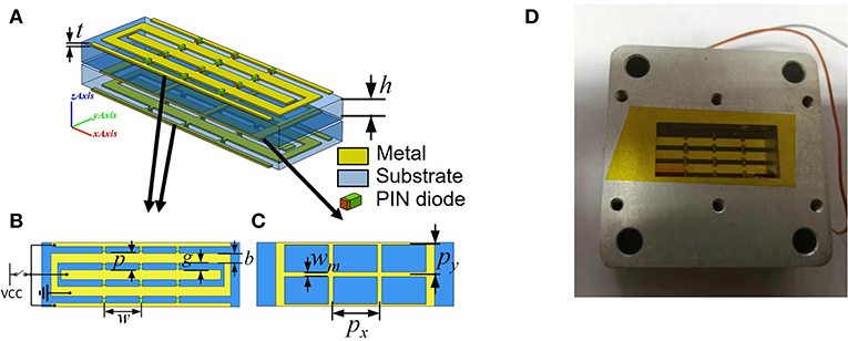
Figure 1. (A) Schematic of the switchable metasurface with three metallic layers and two dielectric layers. Top views of (B) the upper layer and the bottom layer, (C) the middle layer. (D) The photo of our sample with the waveguide.
The state switch of the metasurface is achieved by changing the voltage loaded on the PIN diodes. The diodes are conductive when loaded with forward bias voltage (On-State) that the gratings behave as metallic mesh. Therefor the metasurface is equivalent to three-layered meshes with cutoff frequency much higher than the operational frequency, so that the electromagnetic incidence is strongly reflected. In contrast, the diodes work as capacitors while they are not biased or loaded with reverse bias voltage (Off-State). In this instance, the gratings together with the metallic mesh in the middle layer form a kind of magnetic resonant structure. Although the working frequency is below the cutoff frequency of the mesh in the middle layer that the incident wave cannot directly pass through the structure, near-field coupling between the magnetic modes leads to electromagnetic wave tunneling, similar to the electronic tunneling effect. Therefore, we achieved transmittance manipulation through the control of bias voltage.
FDTD method is employed to calculate the transmission of the metasurface for both states. In the simulation, perfect electric conductor (PEC) boundaries are set at the x and y directions, and absorbing boundary is set at negative z direction. Waveguide port excitation is imposed at positive z direction with the incident wave propagating along z-direction. Figure 2 shows the calculated transmissivity and reflectivity of the metasurface for the two states. When the diode is loaded with forward bias, it is replaced by a resistor with a resistance of 4.2 Ω in the simulation model. As shown in Figure 2A that, for on-state, the transmissivity is <1% and the reflectivity is more than 88%, implying that the electromagnetic wave is almost completely reflected back in a broad frequency band from 8 to 12 GHz. Due to the thermal effect of resistance, there is about 10% absorption loss in the on-state. Figure 2B presents the spectrum for off-state when no bias voltage is applied. The diode is replaced by a capacitor with a capacitance of 0.02 pF in simulation. It is observed that the metasurface is perfectly transparent with transmissivity >96% and reflectivity <4% within the band.
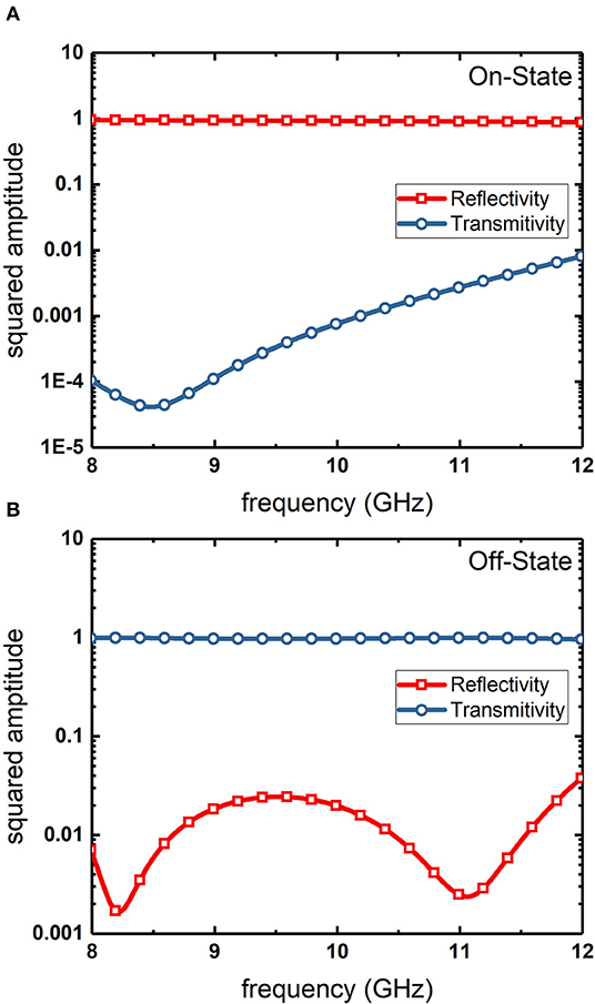
Figure 2. The simulated transmission (blue ring dot lines) and reflection (red square dot lines) spectra of the switchable metasurface when the loaded PIN diodes are (A) on-state and (B) off-state.
In order to verify the proposed switchable metasurface for wide-band electromagnetic manipulation, we fabricate the microwave samples by printed circuit board (PCB) technology, as shown in Figure 1D. Taconic TLX-6 is used with a dielectric constant of 2.65, and the geometric parameters of the sample is kept the same as those of simulation model. Then 24 PIN diodes are loaded on the gratings in upper and bottom surfaces. We adopt Aluminum Gallium Arsenide(AlGaAs) flip-chip PIN diodes(MA4AGP907) because of their small geometry and junction capacitance. When applied with forward bias voltage, the diode is equivalent to a resistor with a resistance of 4.2 Ω at 10 GHz, otherwise it behaves as a capacitor with a capacitance of 0.02 pF. The electrodes are leaded from gratings to impose the bias voltage (shown in Figure 1B). The metasurface is placed in standard waveguide with a length of 22.86 mm and a width of 10.16 mm. Then the waveguide is connected to the vector network analyzer (PNA52224) with a coaxial-to-waveguide converter. By measuring the S parameters, we extract the transmissivity and reflectivity of the sample. Figure 3 shows the experimental results for the two states which are in good agreement with the simulation results, confirming the wide-band control of electromagnetic transparency from the metasurface.
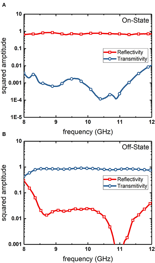
Figure 3. The measured transmission (blue ring dot lines) and reflection (red square dot lines) spectra of the switchable metasurface when the loaded PIN diodes are (A) on-state and (B) off-state.
The bandwidth and efficiency are key points to the electromagnetic wave control. It has been proved that the working bandwidth can be broadened by near-field coupling of resonance modes between adjacent layers [41]. Due to the mutual coupling [44, 52, 53] of magnetic resonance modes, the transmission peak of the metasurface extends to a transmission band as shown in Figures 2B, 3B. The simulated power transmission is above 96% in the frequency range of 8–12 GHz, ant the reflectivity reaches minimum at two resonant frequencies at f = 8.2 and f = 11.1 GHz, while the simulation transmission is above 80% in the frequency range of 8.4–12 GHz, and the reflectivity reaches minimum at two resonant frequencies at f = 8.6 and f = 11.0 GHz. The calculated field distributions provide further insight into the cause of wide-band transparency. Figure 4 shows the spatial distributions of the electric field in the yz plane at the two resonant frequencies. Arrows in the field distributions represent the direction of the electric field vector, with their size and color indicating the scale of the field. It can be read from the color bar that the near-field electric field is magnified six times at these two frequencies of perfect transparency, while the magnitude of plane wave incidence is set as unit. It also can be seen from the field distributions that the y component of electric field is symmetric about the y = 0 plane at 8.2 GHz and is antisymmetric at 11.1 GHz. Considering the symmetry of these two modes, we can draw the conclusion that the perfect transparency peaks result from the inter-layer coupling of the magnetic resonance modes.
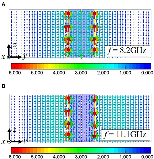
Figure 4. The electric field distribution of (A) the symmetric mode at the perfect transparency frequency 8.2 GHz and (B) the anti-symmetric mode at the perfect transparency frequency 11.1 GHz.
As the bandwidth of transparent state can be broadened by the near-field coupling of the resonance modes in the metasurface, the coupling coefficient can be adjusted by metallic mesh in the middle layer. Inspired by tight binding theory, the weaker the coupling is, the smaller is the energy difference between symmetric and antisymmetric states, vice versa, the stronger the coupling is, the larger is the energy difference. Therefore, it provides a way to control the bandwidth of electromagnetic transparency by adjusting the mesh size in the middle layer. For demonstration, the transmission spectra of wm = 0.5, 0.7, 1.0 mm are calculated and shown in Figure 5. As the value of wm increases, the transparency bandwidth becomes narrower, which agrees well with the theoretical prediction.
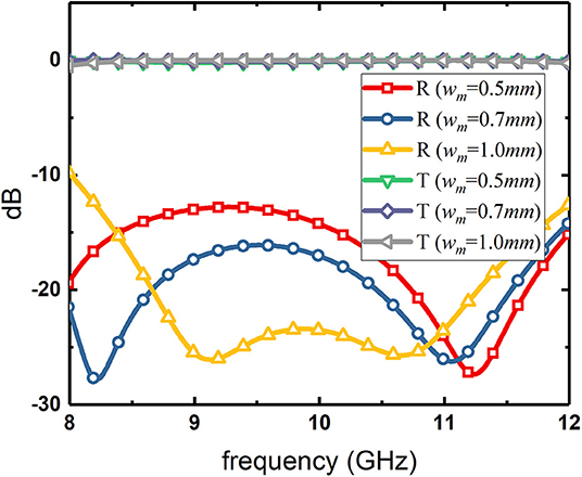
Figure 5. The simulated transmission and reflection spectra of the switchable metasurface when the loaded PIN diodes are off-state. The bandwidth of the transparency can be tuned by the coupling coefficient of the magnetic modes.
In this paper, we have proposed a general scheme to design broadband active metasurface, which switches the transparency and reflection electromagnetic properties by controlling the loaded PIN diodes in the upper surface and bottom surface. The origin of the broadband property is studied in detail, and electric field distributions are presented for the explanation of perfect transparency occurring in the structure. The broadband nature of dynamic manipulation of the transmission and reflection states in the proposed structure is verified both numerically and experimentally. The simulated insertion loss of the metasurface on the transparency state is <0.5 dB within the frequency range 8–12 GHz, which is benefit from evanescent coupling and hybridization of the magnetic resonate modes. The simulated transmission of the metasurface on the reflection state is < -15 dB. The proposed structure is suitable for microwave communication, sensing systems.
The raw data supporting the conclusions of this article will be made available by the authors, without undue reservation, to any qualified researcher.
ZW conceived the idea and supervised the whole study. XL conducted the numerical calculations and performed the experiments. YC derived the theory, carried out the analysis, and drafted the manuscript. All authors contributed to the review of manuscript.
This work was supported by the National Natural Science Foundation of China (Grant Nos. 11674248, 11874285, and 11204218); supported by the Fundamental Research Funds for the Central Universities.
YC was employed by the company Shanghai Mi Xuan Electronic Technology Co., Ltd.
The remaining authors declare that the research was conducted in the absence of any commercial or financial relationships that could be construed as a potential conflict of interest.
1. Born M, Wolf E. Principles of Optics: Electromagnetic Theory of Propagation, Interference and Diffraction of Light. Oxford, Angleterre: Pergamon Press (1980).
2. Engheta N, Ziolkowski RW. Metamaterials: Physics and Engineering Explorations. New York, NY: Wiley-IEEE Press (2006).
3. Cai W, Shalaev V. Optical Metamaterials: Fundamentals and Applications. New York NY: Springer (2009).
4. Yu NF, Genevet P, Kats MA, Aieta F, Tetienne JP, Capasso F, et al. Light propagation with phase discontinuities: generalized laws of reflection and refraction. Science. (2011) 334:333–7. doi: 10.1126/science.1210713
5. Aieta F, Genevet P, Yu NF, Kats MA, Gaburro Z, Capasso F. Out-of-plane reflection and refraction of light by anisotropic optical antenna metasurfaces with phase discontinuities. Nano Lett. (2012) 12:1702–6. doi: 10.1021/nl300204s
6. Yu NF, Capasso F. Flat optics with designer metasurfaces. Nat Mater. (2014) 13:139–50. doi: 10.1038/nmat3839
7. Chen HT, Taylor AJ, Yu NF. A review of metasurfaces: physics and applications. Rep Progr Phys. (2016) 79:076401. doi: 10.1088/0034-4885/79/7/076401
8. Glybovski SB, Tretyakov SA, Belov PA, Kivshar YS, Simovski CR. Metasurfaces: from microwaves to visible. Phys Rep. (2016) 634:1–72. doi: 10.1016/j.physrep.2016.04.004
9. Zhang L, Mei ST, Huang K, Qiu CW. Advances in full control of electromagnetic waves with metasurfaces. Adv Opt Mater. (2016) 4:818–33. doi: 10.1002/adom.201500690
10. Genevet P, Capasso F, Aieta F, Khorasaninejad M, Devlin R. Recent advances in planar optics: from plasmonic to dielectric metasurfaces. Optica. (2017) 4:139–52. doi: 10.1364/OPTICA.4.000139
11. Chen SQ, Li Z, Zhang YB, Cheng H, Tian JG. Phase manipulation of electromagnetic waves with metasurfaces and its applications in nanophotonics. Adv Opt Mater. (2018) 6:1800104. doi: 10.1002/adom.201800104
12. Luo XG. Subwavelength artificial structures: opening a new era for engineering optics. Adv Mater. (2019) 31:1804680. doi: 10.1002/adma.201804680
13. Sun SL, He Q, Hao JM, Xiao SY, Zhou L. Electromagnetic metasurfaces: physics and applications. Adv Opt Photon. (2019) 11:380–479. doi: 10.1364/AOP.11.000380
14. Chen HT, Padilla WJ, Zide JMO, Gossard AC, Taylor AJ, Averitt RD. Active terahertz metamaterial devices. Nature. (2006) 444:597–600. doi: 10.1038/nature05343
15. Chowdhury DR, Azad AK, Zhang WL, Singh R. Near field coupling in passive and active terahertz metamaterial devices. IEEE Trans Terahertz Sci Technol. (2014) 4:400–. doi: 10.1109/TTHZ.2014.2312771
16. Ma X, Pan W, Huang C, Pu M, Wang Y, Zhao B, et al. An active metamaterial for polarization manipulating. Adv Opt Mater. (2014) 2:945–9. doi: 10.1002/adom.201400212
17. Qiao S, Zhang YX, Liang SX, Sun LL, Sun H, Xu GQ, et al. Multi-band terahertz active device with complementary metamaterial. J Appl Phys. (2015) 118:123106. doi: 10.1063/1.4931583
18. Wang DC, Zhang LC, Gu YH, Mehmood MQ, Gong YD, Srivastava A, et al. Switchable ultrathin quarter-wave plate in terahertz using active phase-change metasurface. Sci Rep. (2015) 5:15020. doi: 10.1038/srep15020
19. Xu HX, Sun SL, Tang SW, Ma SJ, He Q, Wang GM, et al. Dynamical control on helicity of electromagnetic waves by tunable metasurfaces. Sci Rep. (2016) 6:27503. doi: 10.1038/srep27503
20. Liu F, Tsilipakos O, Pitilakis A, Tasolamprou AC, Mirmoosa MS, Kantartzis NV, et al. Intelligent metasurfaces with continuously tunable local surface impedance for multiple reconfigurable functions. Phys Rev Appl. (2019) 11:044024. doi: 10.1103/PhysRevApplied.11.044024
21. Li Y, Lin J, Guo HJ, Sun WJ, Xiao SY, Zhou L. A tunable metasurface with switchable functionalities: from perfect transparency to perfect absorption. Adv Opt Mater. (2020) 8:1901548. doi: 10.1002/adom.201901548
22. Wu ZL, Chen XD, Wang MS, Dong JW, Zheng YB. High-performance ultrathin active chiral metamaterials. ACS Nano. (2018) 12:5030–41. doi: 10.1021/acsnano.8b02566
23. Fan YC, Shen NH, Zhang FL, Zhao Q, Wei ZY, Zhang P, et al. Photoexcited graphene metasurfaces: significantly enhanced and tunable magnetic resonances. ACS Photon. (2018) 5:1612–8. doi: 10.1021/acsphotonics.8b00057
24. Fan YC, Shen NH, Zhang FL, Wei ZY, Li HQ, Zhao Q, et al. Electrically tunable goos-hanchen effect with graphene in the terahertz regime. Adv Opt Mater. (2016) 4:1824–8. doi: 10.1002/adom.201600303
25. Chu QQ, Song ZY, Liu QH. Omnidirectional tunable terahertz analog of electromagnetically induced transparency realized by isotropic vanadium dioxide metasurfaces. Appl Phys Expr. (2018) 11:082203. doi: 10.7567/APEX.11.082203
26. Wang WH, Song ZY. Multipole plasmons in graphene nanoellipses. Phys B Condens Matter. (2018) 530:142–6. doi: 10.1016/j.physb.2017.11.038
27. Song ZY, Chen AP, Zhang JH, Wang JY. Integrated metamaterial with functionalities of absorption and electromagnetically induced transparency. Opt Exp. (2019) 27:25196–204. doi: 10.1364/OE.27.025196
28. Wei ML, Song ZY, Deng YD, Liu YN, Chen Q. Large-angle mid-infrared absorption switch enabled by polarization-independent GST metasurfaces. Mater Lett. (2019) 236:350–3. doi: 10.1016/j.matlet.2018.10.136
29. Liu LX, Zhang XQ, Kenney M, Su XQ, Xu NN, Ouyang CM, et al. Broadband metasurfaces with simultaneous control of phase and amplitude. Adv Mater. (2014) 26:5031–6. doi: 10.1002/adma.201401484
30. Ding F, Wang ZX, He SL, Shalaev VM, Kildishev AV. Broadband high-efficiency half-wave plate: a supercell-based plasmonic metasurface approach. ACS Nano. (2015) 9:4111–9. doi: 10.1021/acsnano.5b00218
31. Wang SM, Wu PC, Su VC, Lai YC, Chu CH, Chen JW, et al. Broadband achromatic optical metasurface devices. Nat Commun. (2017) 8:187. doi: 10.1038/s41467-017-00166-7
32. Fan RH, Xiong B, Peng RW, Wang M. Constructing metastructures with broadband electromagnetic functionality. Adv Mater. (2019) 1904646. doi: 10.1002/adma.201904646
33. Fan YC, Tu LQ, Zhang FL, Fu QH, Zhang ZR, Wei ZY, et al. Broadband terahertz absorption in graphene-embedded photonic crystals. Plasmonics. (2018) 13:1153–8. doi: 10.1007/s11468-017-0615-0
34. Ebbesen TW, Lezec HJ, Ghaemi HF, Thio T, Wolff PA. Extraordinary optical transmission through sub-wavelength hole arrays. Nature. (1998) 391:667–9. doi: 10.1038/35570
35. Barnes WL, Dereux A, Ebbesen TW. Surface plasmon subwavelength optics. Nature. (2003) 424:824–30. doi: 10.1038/nature01937
36. de Abajo FJG. Colloquium: light scattering by particle and hole arrays. Rev Mod Phys. (2007) 79:1267–90. doi: 10.1103/RevModPhys.79.1267
37. Garcia-Vidal FJ, Martin-Moreno L, Ebbesen TW, Kuipers L. Light passing through subwavelength apertures. Rev Mod Phys. (2010) 82:729–87. doi: 10.1103/RevModPhys.82.729
38. Carretero-Palacios S, Garcia-Vidal FJ, Martin-Moreno L, Rodrigo SG. Effect of film thickness and dielectric environment on optical transmission through subwavelength holes. Phys Rev B. (2012) 85:035417. doi: 10.1103/PhysRevB.85.035417
39. Ruan ZC, Qiu M. Enhanced transmission through periodic arrays of subwavelength holes: The role of localized waveguide resonances. Phys Rev Lett. (2006) 96:233901. doi: 10.1103/PhysRevLett.96.233901
40. Wei ZY, Fu JX, Cao Y, Wu C, Li HQ. The impact of local resonance on the enhanced transmission and dispersion of surface resonances. Photon Nanostruct Fund Appl. (2010) 8:94–101. doi: 10.1016/j.photonics.2009.10.001
41. Wei ZY, Cao Y, Fan YC, Yu X, Li HQ. Broadband transparency achieved with the stacked metallic multi-layers perforated with coaxial annular apertures. Opt Exp. (2011) 19:21425–31. doi: 10.1364/OE.19.021425
42. Wei ZY, Cao Y, Fan YC, Yu X, Li HQ. Broadband polarization transformation via enhanced asymmetric transmission through arrays of twisted complementary split-ring resonators. Appl Phys Lett. (2011) 99:221907. doi: 10.1063/1.3664774
43. Wei ZY, Cao Y, Su XP, Gong ZJ, Long Y, Li HQ. Highly efficient beam steering with a transparent metasurface. Opt Exp. (2013) 21:10739–45. doi: 10.1364/OE.21.010739
44. Cheng KY, Wei ZY, Fan YC, Zhang XM, Wu C, Li HQ. Realizing broadband transparency via manipulating the hybrid coupling modes in metasurfaces for high-efficiency metalens. Adv Opt Mater. (2019) 7:1900016. doi: 10.1002/adom.201900016
45. Cong LQ, Xu NN, Gu JQ, Singh R, Han JG, Zhang WL. Highly flexible broadband terahertz metamaterial quarter-wave plate. Laser Photon Rev. (2014) 8:626–32. doi: 10.1002/lpor.201300205
46. Fan RH, Zhou Y, Ren XP, Peng RW, Jiang SC, Xu DH, et al. Freely tunable broadband polarization rotator for terahertz waves. Adv Mater. (2015) 27:1201–6. doi: 10.1002/adma.201404981
47. Sievenpiper D, Zhang L, Broas R, Alexopolous N, Yablonovitch E. High-impedance electromagnetic surfaces with a forbidden frequency band. IEEE Trans Microwave Theory Techn. (1999) 47:2059–74. doi: 10.1109/22.798001
48. Zhou L, Wen W, Chan C, Sheng P. Multiband subwavelength magnetic reflectors based on fractals. Appl Phys Lett. (2003) 83:3257–9. doi: 10.1063/1.1622122
49. Zhou L, Li HQ, Qin YQ, Wei ZY, Chan CT. Directive emissions from subwavelength metamaterial-based cavities. Appl Phys Lett. (2005) 86:101101. doi: 10.1063/1.1881797
50. Wei ZY, Li HQ, Cao Y, Wu C, Ren JZ, Hang ZH, et al. Spatially coherent surface resonance states derived from magnetic resonances. New J Phys. (2010) 12:093020. doi: 10.1088/1367-2630/12/9/093020
51. Wei ZY, Li HQ, Wu C, Cao Y, Ren JZ, Hang ZH, et al. Anomalous reflection from hybrid metamaterial slab. Opt Exp. (2010) 18:12119–26. doi: 10.1364/OE.18.012119
52. Tassin P, Zhang L, Zhao RK, Jain A, Koschny T, Soukoulis CM. Electromagnetically induced transparency and absorption in metamaterials: the radiating two-oscillator model and its experimental confirmation. Phys Rev Let. (2012) 109:187401. doi: 10.1103/PhysRevLett.109.187401
Keywords: metasurface, switchable, broadband, high efficiency, PIN diode
Citation: Wei Z, Liu X and Cao Y (2020) Switchable Metasurface With Broadband and Highly Efficient Electromagnetic Functionality. Front. Phys. 8:90. doi: 10.3389/fphy.2020.00090
Received: 05 February 2020; Accepted: 12 March 2020;
Published: 03 April 2020.
Edited by:
Yuancheng Fan, Northwestern Polytechnical University, ChinaReviewed by:
Zhengyong Song, Xiamen University, ChinaCopyright © 2020 Wei, Liu and Cao. This is an open-access article distributed under the terms of the Creative Commons Attribution License (CC BY). The use, distribution or reproduction in other forums is permitted, provided the original author(s) and the copyright owner(s) are credited and that the original publication in this journal is cited, in accordance with accepted academic practice. No use, distribution or reproduction is permitted which does not comply with these terms.
*Correspondence: Zeyong Wei, d2VpemV5b25nQHRvbmdqaS5lZHUuY24=; Yang Cao, Y2FveWFuZzg1QDE2My5jb20=
Disclaimer: All claims expressed in this article are solely those of the authors and do not necessarily represent those of their affiliated organizations, or those of the publisher, the editors and the reviewers. Any product that may be evaluated in this article or claim that may be made by its manufacturer is not guaranteed or endorsed by the publisher.
Research integrity at Frontiers

Learn more about the work of our research integrity team to safeguard the quality of each article we publish.