 Jiaqi Wang
 Zhengkun Xing2,3
 Xia Chen
 Zhenzhou Cheng
94% of researchers rate our articles as excellent or good
Learn more about the work of our research integrity team to safeguard the quality of each article we publish.
Find out more
MINI REVIEW article
Front. Phys., 21 February 2020
Sec. Optics and Photonics
Volume 8 - 2020 | https://doi.org/10.3389/fphy.2020.00037
This article is part of the Research TopicElectronics and Optoelectronics of Graphene and Related 2D MaterialsView all 5 articles
Graphene is a two-dimensional material with numerous intriguing optical properties, such that graphene photonic devices have attracted great interest for sensing and communication applications. However, surface-illuminated graphene photonic devices usually suffer from weak light-matter interactions due to the atomic-layer thickness of graphene, seriously limiting the performances of such devices. To tackle this problem, waveguide-integrated graphene photonic devices have been demonstrated since 2010, which offer the advantage of much longer interaction length between the evanescent field of the optical waveguide and graphene than the surface-illuminated devices. Moreover, the fabrication of waveguide-integrated graphene photonic devices is compatible with CMOS technology, allowing potentially low-cost and high-density on-chip integration. To date, a tremendous interest is growing in the hybrid integration platform composed of graphene and silicon photonic integrated circuits. In this paper, we review the recent progress in waveguide-integrated graphene photonic devices and their applications in sensing and communication.
Graphene has fascinating optical properties for developing photonic devices [1]. First, graphene has a broad spectral band and tunable optical absorption from visible light to the mid-infrared wavelengths because of the linear and zero-bandgap energy band diagram, which is suitable for developing broadband saturable absorbers for ultrafast lasers [2–4]. Second, the electron mobility of graphene could be as large as 200,000 cm2/Vs [5], which is promising for realizing high-speed electro-optic modulators and photodetectors. Third, graphene photonic devices are promising for biochemical sensing applications since graphene has huge adsorption capacity due to the large specific surface area of the monolayer carbon atoms. Moreover, the adsorbed chemical molecules can change the local carrier density of graphene by electron transport and therefore change the optical properties of the photonic devices [6–8]. However, the light absorption of graphene photonic devices based on surface-illuminated geometries is insufficient due to the weak light-matter interaction in the atomic-layer-thick material.
To enhance the light-matter interaction in graphene photonic devices, researchers have proposed to integrate graphene with various photonic structures, such as plasmonic structures [9, 10], optical fibers [11], and photonic integrated circuits (PICs) [12, 13]. Among them, by integrating graphene with PICs, the light-matter interaction can be dramatically enhanced through the coupling of the evanescent field of the optical waveguide. Besides, compared with other configurations, the fabrication process of waveguide-integrated graphene photonic devices is fully CMOS-compatible, which can potentially bring us high-density integration at a low cost. Therefore, numerous waveguide-integrated graphene photonic devices have been widely studied since 2010, for example, broadband polarizers [14], saturable absorbers [15], modulators [16, 17], and photodetectors [18].
Due to the above mentioned merits, the graphene-on-silicon PICs provide an excellent platform for developing on-chip applications of information and communications technology (ICT). The rapid development of 5G telecommunication and internet over things (IoTs) requires up to 50 billion connected devices in use by 2020 [1], which will demand an operation speed larger than 25 Gb s−1 and power consumption lower than 1 pJ bit−1 for key components [19], such as photodetectors and modulators. According to the statistics, the global silicon photonics market (including various applications, such as data center, communications, military, medical science, and sensing) was valued with USD 0.8 billion in 2018 and is expected to increase to USD 2.0 billion by 2023 [20]. Graphene's optical properties may help improve optoelectronic performances of the conventional PICs for meeting the requirement of the quickly developing ICT market. For example, the plasma dispersion effect induced by carrier injection or depletion may limit the speed of chip-integrated optical modulation up to 50 GHz, while the integration of graphene on silicon devices is expected to boost the modulation speed up to 500 GHz [5]. Besides, the integration of graphene can increase the devices' adsorption capacities to chemical molecules which can enhance the sensitivities of on-chip chemical sensors. As a result, the study of waveguide-integrated graphene photonic devices opens up a new way for on-chip optical sensing and communication applications for the next-generation ICT.
In this paper, we introduce the recent progress in waveguide-integrated graphene photonic devices for sensing and communication applications. The design principle of waveguide-integrated graphene photonic devices is introduced in section Design Principle of Waveguide-Integrated Graphene Photonic Devices. Then, in section Waveguide-Integrated Graphene Photonic Devices for Sensing Applications, we review the progress in waveguide-integrated graphene devices for sensing applications, especially the waveguide-integrated graphene biochemical sensors. In section Waveguide-Integrated Graphene Photonic Devices for Communication Applications, we introduce the waveguide-integrated graphene devices for optical communication applications, namely, electro-optical modulators and photodetectors. Finally, we summarize the paper in section Summary and Prospect.
The optical properties of graphene can be described in terms of optical conductivity (σ) which is calculated by using the Kubo model [21]
where h is Planck constant, Ω is the optical frequency, ω is the energy of the relativistic Landau levels, Δ is the excitonic gap of Landau level energies, nF(ω) is the Fermi distribution function, and Γ is the scattering rate. By assuming a finite thickness (d) to the monolayer graphene, the complex relative permittivity of graphene can be deduced from [21]
where ε0 is the relative permittivity of vacuum. The monolayer graphene is a broadband absorber with a 2.3% absorption of normally incident light as a consequence of its gapless energy band diagram. By integrating graphene on the surface of an optical waveguide, the optical absorption can increase toward 100% via the evanescent field coupling. By applying the relative permittivity in a commercial software simulator (e.g., COMSOL Multiphysics), the graphene-on-waveguide absorption coefficient can be calculated. Based on this method, the optical absorption of graphene can be theoretically optimized by designing the waveguide structure and tailoring the length of graphene integrated on the surface of the waveguide [12, 13]. On the other hand, when the Fermi level of graphene is tuned optically or electrically beyond half of the photon energy, graphene becomes transparent due to the Pauli blocking effect, leading to the significant change of the refractive index (RI) and phase shift of the input light. After becoming transparent, graphene also exhibits high non-linearity according to previous theoretical and experimental studies [22–24]. Therefore, by tuning the Fermi level of graphene with chemical doping methods or an external electrical field, waveguide-integrated graphene devices can be developed for chemical sensors and electro-optic modulators, which will be discussed in the following sections.
Graphene's tunable conductivity has been explored for chemical sensing, which has widespread applications, ranging from toxic gas detection for industrial safety to greenhouse gas detection for environmental monitoring. Due to the linear and gapless energy band diagram, graphene has a low carrier density of states near the Dirac point, so the adsorbed molecules acting as donors or acceptors can lead to a drastic change of the conductivity, as shown in Figure 1A. At this point, the adsorbed molecules can induce chemical doping into the local graphene and change its conductivity, which alternates the absorption and phase shift of the input light. Besides, the sensitivity of graphene-based chemical sensing is further improved by its two-dimensional (2D) nature, which results in the large adsorption capacity of graphene. Moreover, compared with early studies of graphene biochemical sensors with the detection of electrical conductivity [6], optical sensors have advantages of high sensitivity, high chemical selectivity, and immunity to electromagnetic interference. Graphene optical sensors have been investigated based on several mechanisms. For example, by coating graphene on the surface of a thin metallic film [25, 26], the sensitivity of conventional surface plasmon resonance sensors can be improved due to the enhanced molecule adsorption by graphene. Or by patterning graphene into nanostructures with electron beam lithography and oxygen plasma etching, localized surface plasmon resonances can be excited [8], which are sensitive to the adsorption of molecules.
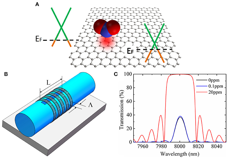
Figure 1. Design of graphene-based photonic chemical sensors. (A) Schematic of the variation of Fermi level induced by the adsorbed molecules on graphene. (B) Design of the silicon fiber-integrated graphene photonic gas sensor. (C) Reflection spectra of the graphene Bragg grating structure for sensing NO2 gas. The black, blue, and red curves represent the Bragg grating reflection spectra at 0, 0.1, and 20 ppm NO2 gas concentrations, respectively. Figures 1B,C are reprinted with permission from Ref. [7]. Copyright © 2019 IEEE.
Meanwhile, the development of waveguide-based graphene optical sensors has attracted much attention, which can improve the sensitivity and add more functionality to the conventional waveguide-based optical sensors. Especially, by integrating graphene and graphene oxide (GO) [27] on side-polished fibers [28], fused tapers [29], interferometers [30], and fiber microknots [31], various graphene biochemical sensors have been demonstrated. Compared with evanescent-wave devices based on microfibers, waveguide-integrated devices offer smaller footprints. Crowe et al. [32] studied light-matter interactions in graphene-based silicon-on-insulator (SOI) racetrack cavity resonators and by optimizing the thickness of the separation spacer layer between graphene and the waveguide, the maximum sensitivity can be achieved. Lim et al. [33] demonstrated a humidity sensor by integrating GO on the SU-8 waveguide. Due to the influence of the water content on the dielectric properties of the GO film, the optical absorption decreases linearly with increasing humidity. Maliakal et al. [34] demonstrated waveguide-integrated chemical sensors by integrating graphene on gated SOI waveguides. A reversible optical attenuation change appears when these devices interact with iodine and ammonia. Cheng et al. [35] and Wang et al. [7] studied the silicon waveguide-integrated and silicon fiber-integrated graphene photonic devices for gas sensing applications in the mid-infrared wavelengths. They proposed using slot waveguides and fiber structures to further increase graphene-light interactions to improve sensors' sensitivities, as shown in Figure 1B. The adsorbed gas molecules can induce chemical doping to graphene and change the effective RI of the graphene Bragg grating structure, leading to the increase in the spectral bandwidth of the central reflection band of the Bragg grating, which is proportional to the concentration of the gas molecules, as shown in Figure 1C.
Graphene's photonic properties give several complementarities over silicon photonics, which makes waveguide-integrated graphene photonic devices promising for communication applications. For example, as the graphene-on-waveguide absorption coefficient is determined by the superimposed area between graphene and the waveguide mode, by integrating graphene on a multimode waveguide, Xing et al. [36] developed mode-division multiplexers based on TE1-mode-pass and TE2-mode-pass filters, as shown in Figure 2A. Moreover, the graphene-on-waveguide absorption is polarization-dependent [38]. Based on the polarization-dependent optical absorption loss, Xing et al. [39] theoretically proposed an on-chip polarizer based on graphene-on-silicon nanowires by tailoring the electric-field distributions on the surface of a silicon nanowire with different polarizations. Besides, Wang et al. [15] demonstrated an ultra-compact waveguide-integrated saturable absorber by integrating graphene on the silicon slot waveguide, which has the advantages of enhanced light-matter interactions and large modulation depth, being suitable for developing on-chip ultrafast lasers, as shown in the scanning electron microscopy (SEM) image of Figure 2B.
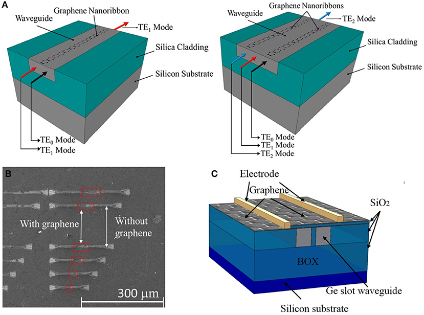
Figure 2. Waveguide-integrated graphene photonic devices. (A) Schematic of the waveguide-integrated graphene TE1-mode-pass and TE2-mode-pass filters. (B) SEM image of the graphene-on-silicon slot waveguide saturable absorber. (C) Schematic of the dual-layer graphene-on-Ge slot waveguide modulator. A is reprinted with permission from Ref. [36]. Copyright © 2019 Optical Society of America. B is reprinted with permission from Ref. [15]. Copyright © 2019 IOP Publishing. C is reprinted with permission from Ref. [37]. Copyright © 2019 Optical Society of America.
The tunable optical properties of graphene can enable light modulation and detection in one chip. High-speed, wide-bandwidth, low-power-consumption, small-footprint, and CMOS-compatible electro-optic modulators are desirable in the fields of optical communication and optical interconnects. During the past few years, waveguide-integrated graphene modulators have been extensively studied to achieve the above-mentioned characteristics. Waveguide-integrated graphene modulators can be classified into two categories, namely, electro-absorption modulators and electro-refractive modulators. For the electro-absorption modulation, it utilizes the change in the optical absorption of graphene induced by the shift of Fermi level produced by electrical gating [40]. Giambra et al. [41] demonstrated a broadband electro-absorption modulator with 29 GHz bandwidth by integrating the dual-layer graphene capacitor on the passive SOI waveguide. Besides the dual-layer graphene capacitor, Shu et al. [42], Hu et al. [43], and Sorianello et al. [44] demonstrated the graphene-oxide-silicon capacitor-based waveguide-integrated modulators, in which the gate voltage is applied through the intentionally doped silicon waveguide. Apart from passive straight waveguide structures, the hybrid plasmonic waveguide-integrated modulators were demonstrated with potential for achieving high modulation depth. Ansell et al. [45] utilized a nanostructured plasmonic waveguide to increase graphene interaction with light, achieving a modulation depth of >0.03 dB μm−1 in an active region of 10 μm2. Ding et al. [46] demonstrated efficient electro-absorption modulation based on leaky mode plasmonic slot waveguides integrated on the SOI platform, which shows an absorption loss tunability of 0.13 dB μm−1.
Although the graphene-based electro-absorption modulators hold superb merits of relatively low drive voltages and high speed, these modulators may suffer from serious signal-to-noise ratio degradation when applied in long-haul communications. In order to meet the needs of phase-shift keying formats, graphene-based electro-refractive modulation has been demonstrated, which utilizes the change in the real part of the dielectric constant of graphene by applying an electric field to alternate the phase of the light propagating in the waveguide [47]. By using advanced fabrication processes, Sorianello et al. [48] reported an electro-refractive modulator based on a graphene-insulator-silicon capacitor integrated on the Mach-Zehnder interferometer configuration. The device has a modulation efficiency of 2.8 Vmm, with a static modulation depth of 35 dB and modulator bandwidth of 5 GHz. To further improve the modulators' efficiency, Wang et al. [37] proposed to use vertical germanium (Ge) slot waveguides to enhance the light intensity and reduce the confinement of the optical mode in the slot nanostructure, as shown in Figure 2C. By changing the Fermi level of graphene, the variation in the effective RI of the graphene-on-slot waveguide is two times as large as that of the conventional graphene-on-rib waveguide.
With properties of high carrier mobility and zero energy band gap, graphene is also suitable for developing high-speed and broadband photodetectors. Early demonstrations are based on normally incident graphene field-effect transistor configurations with responsivities around several mA/W [5, 49], limited by the 2.3% optical absorption of monolayer graphene. Then, graphene has been proposed and demonstrated to be integrated with microcavities [50] and plasmonic structures [10] to enhance the optical interaction. However, these structures are relatively complicated and have restricted spectral bandwidths. Waveguide-integrated graphene photodetectors have been demonstrated since 2013 [51–53], in which the optical absorption is enhanced by the evanescent field interaction along the silicon waveguides. Shiue et al. [54] introduced a 2D heterostructure consisting of monolayer graphene encapsulated by hexagonal boron nitride on the silicon waveguide, which reaches a responsivity of 0.36 A/W with 42 GHz bandwidth. Moreover, the performance of graphene photodetectors could be improved by using sophisticated waveguide structures [55]. Zhou et al. [56] demonstrated an enhanced photoresponsivity by integrating graphene with the slow-light photonic crystal waveguide to form a graphene-silicon Schottky-like photodetector. Schuler et al. [57] reported a graphene photodetector based on a silicon photonic crystal defect waveguide combined with a split-gate electrode to create a p–n junction in the vicinity of the optical absorption area. Li et al. [58] integrated graphene on the photonic crystal waveguide with a lateral p-i-n configuration which creates a built-in electrical field and enables the bias-free photodetection. Besides photonic crystal waveguides, plasmonic nanostructures can also provide the field enhancing effect. Ma et al. [59] integrated nanosized metallic structures on the silicon channel waveguide and realized a responsivity of 0.5 A/W and a fast photoresponse of 110 GHz with a 6 μm-long device footprint. Apart from silicon waveguides, people have demonstrated graphene photodetectors based on other waveguides. For example, Wang et al. [60] reported the first graphene photodetector based on silicon nitride waveguide with a maximum internal responsivity of 126 mA/W in the telecommunication band. Later, photoconductor graphene photodetectors based on glass waveguide were reported [61] in 2016.
In summary, we review the recent progress in waveguide-integrated graphene photonic devices for sensing and optical communication applications, namely, waveguide-integrated graphene photonic chemical sensors, polarizers, spatial-mode filters, modulators, and photodetectors. In the future, the following topics may be interesting to explore.
First, compared with modulators and photodetectors, the development of waveguide-integrated graphene photonic sensors is still in its infancy. A great deal of previous research mainly focused on fiber and SPR sensors, rather than PICs. Moreover, the effects of doping and defects of graphene need to be deeply investigated for further improving the sensitivity and specificity of graphene-based sensors.
Second, for waveguide-integrated modulators and photodetectors, delicate designs with photonic structures of enhanced light-matter interaction and electrode settings of improved carrier transport are highly demanded in the future. Besides, more efforts need to be made for realizing the low-cost integration of graphene with insulator (namely, silicon nitride and SiO2) waveguides based on the back-end process.
Third, the fabrication process needs to be improved to meet the criteria for wafer process lines. Currently, most reported results are laboratory research using the lift-off method to fabricate metal electrodes, which is not suitable for the large-scale chip manufacturing. A CMOS-compatible metal contact fabrication process is required in the future.
Finally, it is promising to explore the integration of other 2D materials, such as black phosphorus, transition metal dichalcogenides, and hexagonal boron nitride, on a waveguide. By virtue of the extraordinary properties of various 2D materials and their heterostructures [62], it can be expected that the performance of 2D material-silicon hybrid PICs can be future boosted in sensing and communication applications.
JW and ZX organized and wrote the article. ZC and XL supervised the team. All authors discussed and participated in revising the manuscript.
This work was supported in part by the National Natural Science Foundation of China (61805164, 61805175, and 61775149), 111 Project (B17031), the Teaching Reform Research Project of Shenzhen University (JG2019068), the Shenzhen Science and Technology Project (JCYJ20190731195912687).
The authors declare that the research was conducted in the absence of any commercial or financial relationships that could be construed as a potential conflict of interest.
1. Romagnoli M, Sorianello V, Midrio M, Koppens FHL, Huyghebaert C, Neumaier D, et al. Graphene-based integrated photonics for next-generation datacom and telecom. Nat Rev Mater. (2018) 3:392–414. doi: 10.1038/s41578-018-0040-9
2. Bao Q, Zhang H, Wang Y, Ni Z, Yan Y, Shen ZX, et al. Atomic-layer graphene as a saturable absorber for ultrafast pulsed lasers. Adv Funct Mater. (2009) 19:3077–83. doi: 10.1002/adfm.200901007
3. Hasan T, Sun Z, Wang F, Bonaccorso F, Tan PH, Rozhin AG, et al. Nanotube-polymer composites for ultrafast photonics. Adv Mater. (2009) 21:3874–99. doi: 10.1002/adma.200901122
4. Goossens S, Navickaite G, Monasterio C, Gupta S, Piqueras JJ, Pérez R, et al. Broadband image sensor array based on graphene–CMOS integration. Nat Photonics. (2017) 11:366–71. doi: 10.1038/nphoton.2017.75
5. Xia F, Mueller T, Lin Y, Valdes-Garcia A, Avouris P. Ultrafast graphene photodetector. Nat Nanotechnol. (2009) 4:839–43. doi: 10.1038/nnano.2009.292
6. Schedin F, Geim AK, Morozov SV, Hill EW, Blake P, Katsnelson MI, et al. Detection of individual gas molecules adsorbed on graphene. Nat Mater. (2007) 6:652–5. doi: 10.1038/nmat1967
7. Wang J, Chen Y, Geng Y, Hong X, Li X. Theoretical design of mid-infrared graphene optical gas sensor based on slot Si core fiber. IEEE Photonics Technol Lett. (2019) 31:1096–9. doi: 10.1109/LPT.2019.2919427
8. Rodrigo D, Limaj O, Janner D, Etezadi D, García de Abajo FJ, Pruneri V, et al. Mid-infrared plasmonic biosensing with graphene. Science. (2015) 349:165–8. doi: 10.1126/science.aab2051
9. Fang Z, Wang Y, Liu Z, Schlather A, Ajayan PM, Koppens FHL, et al. Plasmon-induced doping of graphene. ACS Nano. (2012) 6:10222–8. doi: 10.1021/nn304028b
10. Echtermeyer TJ, Britnell L, Jasnos PK, Lombardo A, Gorbachev RV, Grigorenko AN, et al. Strong plasmonic enhancement of photovoltage in graphene. Nat Commun. (2011) 2:458. doi: 10.1038/ncomms1464
11. Zhao Y, Li X, Zhou X, Zhang Y. Review on the graphene based optical fiber chemical and biological sensors. Sens Actuat B Chem. (2016) 231:324–40. doi: 10.1016/j.snb.2016.03.026
12. Li H, Anugrah Y, Koester SJ, Li M. Optical absorption in graphene integrated on silicon waveguides. Appl Phys Lett. (2012) 101:111110. doi: 10.1063/1.4752435
13. Gruhler N, Benz C, Jang H, Ahn J-H, Danneau R, Pernice WHP. High-quality Si3N4 circuits as a platform for graphene-based nanophotonic devices. Opt Express. (2013) 21:31678–89. doi: 10.1364/OE.21.031678
14. Bao Q, Zhang H, Wang B, Ni Z, Lim CHY, Wang XY, et al. Broadband graphene polarizer. Nat Photonics. (2011) 5:411–5. doi: 10.1038/nphoton.2011.102
15. Wang J, Liang Z, Chen Y, Geng Y, Hong X, Li X, et al. Saturable absorption in graphene-on-waveguide devices. Appl Phys Express. (2019) 12:032003. doi: 10.7567/1882-0786/ab02ca
16. Liu M, Yin X, Ulin-Avila E, Geng B, Zentgraf T, Ju L, et al. A graphene-based broadband optical modulator. Nature. (2011) 474:64–7. doi: 10.1038/nature10067
17. Liu M, Yin X, Zhang X. Double-layer graphene optical modulator. Nano Lett. (2012) 12:1482–5. doi: 10.1021/nl204202k
18. Schall D, Porschatis C, Otto M, Neumaier D. Graphene photodetectors with a bandwidth >76 GHz fabricated in a 6″ wafer process line. J Phys D Appl Phys. (2017) 50:124004. doi: 10.1088/1361-6463/aa5c67
19. Arakawa Y, Nakamura T, Urino Y, Fujita T. Silicon photonics for next generation system integration platform. IEEE Commun Mag. (2013) 51:72–7. doi: 10.1109/MCOM.2013.6476868
20. Silicon Photonics Market by Product (Transceiver, Switch, Variable Optical Attenuator, Cable, Sensor), Application (Data Center, Telecommunications, Military & Defense, Medical and Life Sciences, Sensing), Component, and Geography - Global Forecast to 2023, Markets and Markets. (2019). Available online at: https://www.marketsandmarkets.com/market-reports/silicon-photonics-116.html
21. Gosciniak J, Tan DTH. Theoretical investigation of graphene-based photonic modulators. Sci Rep. (2013) 3:1897. doi: 10.1038/srep01897
22. Gorbach AV. Nonlinear graphene plasmonics: amplitude equation for surface plasmons. Phys Rev A. (2013) 87:013830. doi: 10.1103/PhysRevA.87.013830
23. Auditore A, Angelis CD, Locatelli A, Boscolo S, Midrio M, Romagnoli M, et al. Graphene sustained nonlinear modes in dielectric waveguides. Opt Lett. (2013) 38:631–3. doi: 10.1364/OL.38.000631
24. Vermeulen N, Castelló-Lurbe D, Khoder M, Pasternak I, Krajewska A, Ciuk T, et al. Graphene's nonlinear-optical physics revealed through exponentially growing self-phase modulation. Nat Commun. (2018) 9:2675. doi: 10.1038/s41467-018-05081-z
25. Wu L, Chu HS, Koh WS, Li EP. Highly sensitive graphene biosensors based on surface plasmon resonance. Opt Express. (2010) 18:14395–400. doi: 10.1364/OE.18.014395
26. Salihoglu O, Balci S, Kocabas C. Plasmon-polaritons on graphene-metal surface and their use in biosensors. Appl Phys Lett. (2012) 100:213110. doi: 10.1063/1.4721453
27. Mishra SK, Tripathi SN, Choudhary V, Gupta BD. SPR based fibre optic ammonia gas sensor utilizing nanocomposite film of PMMA/reduced graphene oxide prepared by in situ polymerization. Sens Actuat B Chem. (2014) 199:190–200. doi: 10.1016/j.snb.2014.03.109
28. Yao BC, Wu Y, Webb DJ, Zhou JH, Rao YJ, Pospori A, et al. Graphene-based D-shaped polymer FBG for highly sensitive erythrocyte detection. IEEE Photon Technol. Lett. (2015) 27:2399–402. doi: 10.1109/LPT.2015.2466614
29. Fu H, Jiang Y, Ding J, Zhang J, Zhang M, Zhu Y, et al. Zinc oxide nanoparticle incorporated graphene oxide as sensing coating for interferometric optical microfiber for ammonia gas detection. Sens Actuat B Chem. (2018) 254:239–47. doi: 10.1016/j.snb.2017.06.067
30. Hao T, Chiang KS. Graphene-based ammonia-gas sensor using in-fiber Mach-Zehnder interferometer. IEEE Photon Technol Lett. (2017) 29:2035–8. doi: 10.1109/LPT.2017.2761981
31. Yu C, Wu Y, Liu X, Yao B, Fu F, Gong Y, et al. Graphene oxide deposited microfiber knot resonator for gas sensing. Opt Mater Express. (2016) 6:727–33. doi: 10.1364/OME.6.000727
32. Crowe IF, Clark N, Hussein S, Towlson B, Whittaker E, Milosevic MM, et al. Determination of the quasi-TE mode (in-plane) graphene linear absorption coefficient via integration with silicon-on-insulator racetrack cavity resonators. Opt Express. (2014) 22:18625–32. doi: 10.1364/OE.22.018625
33. Lim WH, Yap YK, Chong WY, Ahmad H. All-optical graphene oxide humidity sensors. Sensors. (2014) 14:24329–37. doi: 10.3390/s141224329
34. Maliakal A, Husaini S, Reith L, Bollond P, Cabot S, Sheehan P, et al. Graphene planar lightwave circuit sensors for chemical detection. Proc SPIE. (2017) 10107:101070T. doi: 10.1117/12.2252644
35. Cheng Z, Goda K. Design of waveguide-integrated graphene devices for photonic gas sensing. Nanotechnology. (2016) 27:505206. doi: 10.1088/0957-4484/27/50/505206
36. Xing Z, Li C, Han Y, Hu H, Cheng Z, Wang J, et al. Waveguide-integrated graphene spatial mode filters for on-chip mode-division multiplexing. Opt Express. (2019) 27:19188–95. doi: 10.1364/OE.27.019188
37. Wang J, Li Q, Huang D, Liang C, Chen Y, Fang L, et al. Design of graphene-on-germanium waveguide electro-optic modulators at the 2μm wavelength. OSA Contin. (2019) 2:749–58. doi: 10.1364/OSAC.2.000749
38. Cheng Z, Tsang HK, Wang X, Xu K, Xu JB. In-plane optical absorption and free carrier absorption in graphene-on-silicon wdaveguides. IEEE J Sel Top Quantum Electron. (2013) 20:43–8. doi: 10.1109/JSTQE.2013.2263115
39. Xing Z, Li C, Han Y, Hu H, Cheng Z, Liu T. Design of on-chip polarizers based on graphene-on-silicon nanowires. Appl Phys Express. (2019) 12:072001. doi: 10.7567/1882-0786/ab235a
40. Phare CT, Daniel Lee Y-H, Cardenas J, Lipson M. Graphene electro-optic modulator with 30 GHz bandwidth. Nat Photon. (2015) 9:511–4. doi: 10.1038/nphoton.2015.122
41. Giambra MA, Sorianello V, Miseikis V, Marconi S, Montanaro A, Galli P, et al. High-speed double layer graphene electro-absorption modulator on SOI waveguide. Opt Express. (2019) 27:20145–55. doi: 10.1364/OE.27.020145
42. Shu H, Su Z, Huang L, Wu Z, Wang X, Zhang Z, et al. Significantly high modulation efficiency of compact graphene modulator based on silicon waveguide. Sci Rep. (2018) 8:991. doi: 10.1038/s41598-018-19171-x
43. Hu Y, Pantouvaki M, Van Campenhout J, Brems S, Asselberghs I, Huyghebaert C, et al. Broadband 10 Gb/s operation of graphene electro-absorption modulator on silicon. Laser Photonics Rev. (2016) 10:307–16. doi: 10.1002/lpor.201500250
44. Sorianello V, Contestabile G, Midrio M, Pantouvaki M, Asselbergs I, Van Campenhout J, et al. Chirp management in silicon-graphene electro absorption modulators. Opt Express. (2017) 25:19371–81. doi: 10.1364/OE.25.019371
45. Ansell D, Radko IP, Han Z, Rodriguez FJ, Bozhevolnyi SI, Grigorenko AN. Hybrid graphene plasmonic waveguide modulators. Nat Commun. (2015) 6:8846. doi: 10.1038/ncomms9846
46. Ding Y, Guan X, Zhu X, Hu H, Bozhevolnyi SI, Oxenløwe LK, et al. Efficient electro-optic modulation in low-loss graphene-plasmonic slot waveguides. Nanoscale. (2017) 9:15576–81. doi: 10.1039/C7NR05994A
47. Mohsin M, Schall D, Otto M, Chmielak B, Suckow S, Neumaier D. Towards the predicted high performance of waveguide integrated electro-refractive phase modulators based on graphene. IEEE Photon J. (2017) 9:7800507. doi: 10.1109/JPHOT.2016.2641745
48. Sorianello V, Midrio M, Contestabile G, Asselberghs I, Van Campenhout J, Huyghebaert C, et al. Graphene-silicon phase modulators with gigahertz bandwidth. Nat Photon. (2018) 12:40–4. doi: 10.1038/s41566-017-0071-6
49. Mueller T, Xia F, Avouris P. Graphene photodetectors for high-speed optical communications. Nat Photon. (2010) 4:297–301. doi: 10.1038/nphoton.2010.40
50. Furchi M, Urich A, Pospischil A, Lilley G, Unterrainer K, Detz H, et al. Microcavity-integrated graphene photodetector. Nano Lett. (2012) 12:2773–7. doi: 10.1021/nl204512x
51. Pospischil A, Humer M, Furchi MM, Bachmann D, Guider R, Fromherz T, et al. CMOS-compatible graphene photodetector covering all optical communication bands. Nat Photon. (2013) 7:892–6. doi: 10.1038/nphoton.2013.240
52. Gan X, Shiue R-J, Gao Y, Meric I, Heinz TF, Shepard K, et al. Chip-integrated ultrafast graphene photodetector with high responsivity. Nat Photon. (2013) 7:883–7. doi: 10.1038/nphoton.2013.253
53. Wang X, Cheng Z, Xu K, Tsang HK, Xu J-B. High-responsivity graphene/silicon-heterostructure waveguide photodetectors. Nat Photon. (2013) 7:888–91. doi: 10.1038/nphoton.2013.241
54. Shiue R-J, Gao Y, Wang Y, Peng C, Robertson AD, Efetov DK, et al. High-responsivity graphene-boron nitride photodetector and autocorrelator in a silicon photonic integrated circuit. Nano Lett. (2015) 15:7288–93. doi: 10.1021/acs.nanolett.5b02368
55. Wang J, Cheng Z, Chen Z, Wan X, Zhu B, Tsang HK, et al. High-responsivity graphene-on-silicon slot waveguide photodetectors. Nanoscale. (2016) 8:13206–11. doi: 10.1039/C6NR03122F
56. Zhou H, Gu T, McMillan JF, Yu M, Lo G, Kwong D-L, et al. Enhanced photoresponsivity in graphene-silicon slow-light photonic crystal waveguides. Appl Phys Lett. (2016) 108:111106. doi: 10.1063/1.4944414
57. Schuler S, Schall D, Neumaier D, Schwarz B, Watanabe K, Taniguchi T, et al. Graphene photodetector integrated on a photonic crystal defect waveguide. ACS Photon. (2018) 5:4758–63. doi: 10.1021/acsphotonics.8b01128
58. Li T, Mao D, Petrone NW, Grassi R, Hu H, Ding Y, et al. Spatially controlled electrostatic doping in graphene p-i-n junction for hybrid silicon photodiode. NPJ 2D Mater Appl. (2018) 2:36. doi: 10.1038/s41699-018-0080-4
59. Ma P, Salamin Y, Baeuerle B, Josten A, Heni W, Emboras A, et al. Plasmonically enhanced graphene photodetector featuring 100 Gbit/s data reception, high responsivity, and compact size. ACS Photon. (2019) 6:154–61. doi: 10.1021/acsphotonics.8b01234
60. Wang J, Cheng Z, Chen Z, Xu J-B, Tsang HK, Shu C. Graphene photodetector integrated on silicon nitride waveguide. J Appl Phys. (2015) 117:144504. doi: 10.1063/1.4917378
61. Wang G, Dai T, Lvy Z, Hao Y, Yu H, Wang Y, et al. Integrated high responsivity photodetectors based on graphene/glass hybrid waveguide. Opt Lett. (2016) 41:4214–7. doi: 10.1364/OL.41.004214
Keywords: graphene, silicon photonics, saturable absorption, electro-optic modulator, photodetector
Citation: Wang J, Xing Z, Chen X, Cheng Z, Li X and Liu T (2020) Recent Progress in Waveguide-Integrated Graphene Photonic Devices for Sensing and Communication Applications. Front. Phys. 8:37. doi: 10.3389/fphy.2020.00037
Received: 01 October 2019; Accepted: 06 February 2020;
Published: 21 February 2020.
Edited by:
Xinming Li, South China Normal University, ChinaReviewed by:
Costantino De Angelis, University of Brescia, ItalyCopyright © 2020 Wang, Xing, Chen, Cheng, Li and Liu. This is an open-access article distributed under the terms of the Creative Commons Attribution License (CC BY). The use, distribution or reproduction in other forums is permitted, provided the original author(s) and the copyright owner(s) are credited and that the original publication in this journal is cited, in accordance with accepted academic practice. No use, distribution or reproduction is permitted which does not comply with these terms.
*Correspondence: Zhenzhou Cheng, emhlbnpob3VjaGVuZ0B0anUuZWR1LmNu; Xuejin Li, bGl4dWVqaW5Ac3p1LmVkdS5jbg==
Disclaimer: All claims expressed in this article are solely those of the authors and do not necessarily represent those of their affiliated organizations, or those of the publisher, the editors and the reviewers. Any product that may be evaluated in this article or claim that may be made by its manufacturer is not guaranteed or endorsed by the publisher.
Research integrity at Frontiers
Learn more about the work of our research integrity team to safeguard the quality of each article we publish.