
95% of researchers rate our articles as excellent or good
Learn more about the work of our research integrity team to safeguard the quality of each article we publish.
Find out more
REVIEW article
Front. Phys. , 21 June 2019
Sec. Chemical Physics and Physical Chemistry
Volume 7 - 2019 | https://doi.org/10.3389/fphy.2019.00082
This article is part of the Research Topic Toward Sustainable Energy: The Unique Role of Rare Earth Oxides View all 8 articles
 Alok K. Jha*
 Kaname Matsumoto
The lossless transmission of direct electrical currents in superconductors is very often regarded as an “energy superhighway” with greatly enhanced efficiency. With the discovery of high temperature superconductors (HTS) in the late eighties, the prospect of using these materials in efficient and advanced technological applications became very prominent. The elevated operating temperatures as compared to low temperature superconductors (LTS), relaxing cooling requirements, and the gradual development of facile synthesis processes raised hopes for a broad breakthrough of superconductor technology. The impact of superconductor technology on the economy and energy sectors is predicted to be huge if these are utilized on a large scale. The development of superconducting tapes with high critical current density (Jc) is crucial for their use in transmission cables. Many countries these days are running projects to develop wires from these HTS materials and simultaneously field trials are being conducted to assess the feasibility of this technology. These HTS wires can carry electrical currents more than 100 times larger than their conventional counterparts with minimal loss of energy. The increased efficiency of HTS electric power products may result in greatly reduced carbon emissions compared to those resulting from using the conventional alternatives. In order to use the thin films of YBa2Cu3O7−δ (YBCO) and REBCO [RE (rare-earth) = Sm, Gd, Eu etc.], members of the HTS family, for future technological applications, the enhancement of Jc over wide range of temperatures and applied magnetic fields is highly desired. The enhancement of Jc of YBCO and REBCO films has been successfully demonstrated by employing different techniques which include doping by rare-earth atoms, incorporating nanoscale secondary phase inclusions into the REBCO film matrix, decoration of the substrate surface etc. which generate artificial pinning centers (APCs). In this review, the development of the materials engineering aspect that has been conducted over the last two decades to improve the current carrying capability of HTS thin films is presented. The effect of controlled incorporation of APCs through various methods and techniques on the superconducting properties of YBCO and REBCO thin films is presented, heading toward superior performance of such superconducting thin films.
Superconductivity is a phenomenon in which the material in consideration has virtually no resistance to direct electric current. This phenomenon takes place below a certain characteristic temperature, known as critical temperature, or transition temperature (Tc), which is different for different superconductors. Ever since its discovery by Onnes [1], it has been a subject of great interest because of the unique properties it exhibits. In addition to transport of electrical current without any resistance, the superconducting state is also characterized by perfect diamagnetism (χm = −1). The magnetic flux is expelled from the interior of the superconductor at T < Tc. The screening currents are induced in the surface layer of the superconductor which generates a flux density opposite to that of the applied magnetic field. This phenomenon is known as Meissner effect [2].
On the basis of their magnetic properties, superconductors have been broadly classified into two classes:
(a) Type I Superconductor: Type I superconductors expel the magnetic field completely for applied magnetic field (H) smaller than the critical magnetic field (Hc). Above Hc, the material abruptly goes back into the normal state. The variation of magnetization (M) with respect to H for type I and type II superconductors is presented in Figure 1A. Most of the elemental superconductors (e.g., Pb, Hg, Sn, etc.) exhibit type I superconductivity except Nb, V, and Tc [3]. In addition, type I superconductivity is also exhibited by an alloy, TaSi2 [4] and a compound, SiC (with heavy doping of B) [5]. The Tcs for type I superconductors are normally lower (< 10 K). The values of Hc for type I superconductors are in the range of 5–200 mT [3]. Because of their low Tc and Hc values, type I superconductors are of limited use.
(b) Type II Superconductor: Type II superconductors have two critical magnetic fields: Hc1 and Hc2 as depicted in Figure 1A. Below Hc1, the superconductor remains in the Meissner state, completely expelling the magnetic flux from its interior. For H > Hc1 but smaller than Hc2, the magnetic flux starts penetrating the sample in the form of discrete bundles termed “flux lines” and the sample goes into the mixed state (or vortex state). When H becomes > Hc2, the superconductor comes into the normal state. In the vortex state, the specimen comprises of alternating normal and superconducting regions. The normal cores are surrounded by superconducting regions allowing some magnetic field penetration. Type II superconductivity is exhibited by metallic compounds, alloys, and complex oxide ceramics. Type II superconductors have much higher critical magnetic fields as compared to type I superconductors. Also, Type II superconductors can carry much larger current densities while remaining in the superconducting state. Due to the above advantages, type II superconductors have greater potential for practical applications.
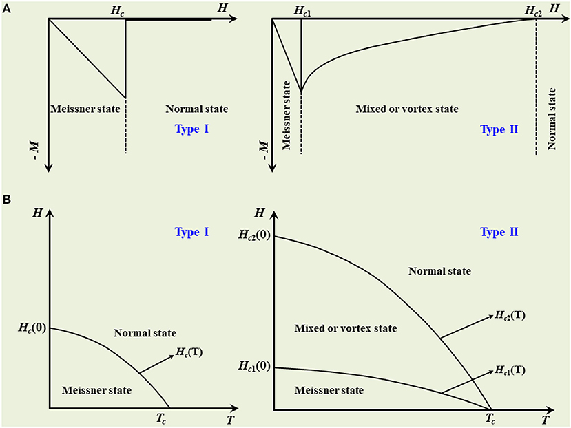
Figure 1. (A) Variation of magnetization as a function of applied magnetic field for type I and type II superconductors. (B) The corresponding H-T phase diagram for type I and type II superconductors.
Apart from the critical temperature (Tc), the critical current density (Jc) is the most relevant parameter of a superconductor which is directly related to its possible use in practical applications [6–8]. Jc in a superconductor is determined by the critical temperature, electronic structure, and the flux pinning mechanism governed by the microscopic defects that are generated naturally or artificially during the growth of the superconducting films. The upper limit of the Jc is determined by splitting of the paired electrons that carry the supercurrent (the so-called Cooper pairs), and Ginzburg-Landau gave an equation to estimate the depairing current density (current density at which splitting of Cooper pairs takes place) Jd [9]:
where Φ0, μ0, λ, and ξ are the flux quantum, permeability in vacuum, the London penetration depth and the Pippard coherence length, respectively. Jc cannot exceed this value even by the optimum vortex pinning [10]. For YBa2Cu3O7−δ (YBCO) and REBCO [RE (rare-earth) = Sm, Gd, Eu etc.] films, Jd at 77 K and zero applied field is estimated to be 40–50 MAcm−2 [11]. This value is quite large but the observed values of Jc are limited to about 10% of Jd. Thus, there is large room for sufficient enhancement of Jc by employing different methodologies.
Figure 1B shows the H-T phase diagrams for type I and type II superconductors. In the mixed state (Hc1 ≤ H ≤ Hc2) of a type II superconductor, the magnetic flux penetrates into the superconducting specimen in the form of small “tubes” called vortices. These vortices have a normal-conducting core and are surrounded by circulating supercurrents generating a magnetic flux quantum Φ0 = h/2e (h being Planck's constant and e being electronic charge). The circular currents make any two vortices repel each other forming an ordered hexagonal lattice called the Abrikosov vortex lattice. If an electrical current is passed through a superconductor in its mixed state, the vortices would experience a Lorentz force, whose density is given by FL = J × μ0H. Due to the influence of this Lorentz force, the vortices start to move in a direction perpendicular to the directions of both the transport current and the applied magnetic field. A schematic representation of this situation is presented in Figure 2. There are, however, some kinds of defects or impurities in superconducting samples, such as dislocations, voids, grain boundaries, etc. which act as pinning centers for vortices and the magnetic flux gets trapped. The force which resists the motion of the vortices under the influence of the Lorentz force is called the pinning force, whose density is termed as pinning forced density (Fp). The flux lines remain stationary, as long as Fp is > FL. When FL exceeds Fp, vortices start moving across the superconductor. If the vortices move with a velocity v, an electric field E = μ0H × v would be generated. Since, both the current and the generated electric field would be parallel, a finite power would be dissipated in the system and the superconductor would lose its ability to sustain dissipation-free current flow.
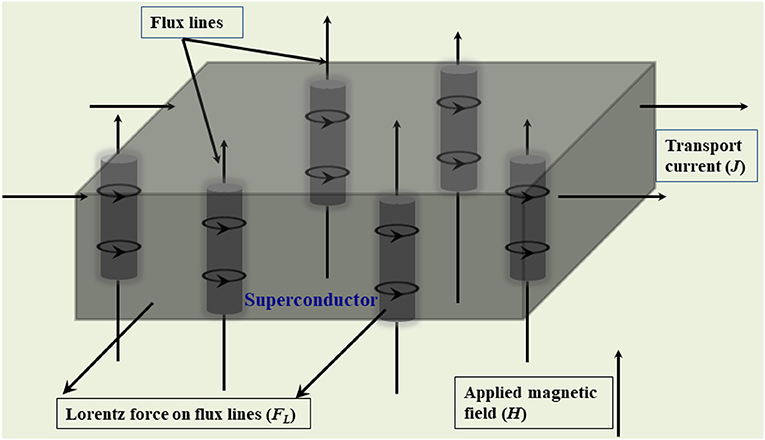
Figure 2. Mixed state in a type II superconductor. Magnetic flux starts penetrating the sample in the form of small “tubes” (vortices), each with quantized flux Φ0 = h/(2e).
The penetration of magnetic flux in a type II superconductor is gradual over a wide range of applied magnetic field. However, the presence of lattice defects prevents the easy entry or exit of the flux lines and the magnetization is irreversible. The presence of lattice defects modifies the vortex structure; vortices may be “pinned” down at the defect sites and no longer free to move. From the energetics point of view, the defect sites are surrounded by an energy barrier which the pinned vortex must climb before it can move. The Lorentz force effectively lowers this barrier and the critical current density of a specimen would reach when the pinning force is balanced by the Lorentz force. At finite temperatures, however, thermal activation also lowers the effective barrier height and gives rise to a strongly temperature dependent critical current.
YBCO belongs to the class of type II superconductors, which are known for their ability to maintain the superconducting properties even at higher applied magnetic fields. YBCO was the first superconductor which was shown to have Tc above the liquid nitrogen temperature (77 K) [12]. The discovery of YBCO fuelled lot of research activities in the field of superconductivity and most of the earlier works were focused on discovering the superconductor which could have an even higher Tc. Subsequently several other superconductors such as Bi2Sr2Ca2Cu3O10+δ [13], Tl2Ba2Ca2Cu3O10 [14], and HgBa2Ca2Cu3O8+δ [15] have been discovered which were found to have Tcs above 77 K. However, among all other cuprate superconductors, YBCO has several advantages over others which include many facile synthesis routes for thin film fabrication and much larger irreversibility field (Hirr).
Hirr of a superconductor is another very important parameter which is defined as the magnetic field at which the resistivity value due to flux motion is significant and the pinning strength goes to zero [16, 17]. The irreversibility line divides the H-T phase diagram of a superconductor into two portions: reversible and irreversible (or hysteretic). The reversible portion of this phase diagram refers to the vortex-liquid state in which vortex movements due to thermal fluctuation are so high that the ordered vortex lattice state (referred by irreversible portion of the phase diagram) is destroyed [18, 19]. Thus, the irreversibility line or the melting line demarcates the solid-liquid phases of the vortex matter and it is highly desired to shift this line toward higher H-T regime by artificial pinning center (APC) technology [6, 8, 20, 21]. Figure 3 shows the comparison of the irreversibility lines of various superconductors which include superconducting alloys, metallic compounds, MgB2, and high temperature superconductors (HTS). The coated conductor technology employing APC incorporation in superconducting REBCO matrix is set to usher new frontiers of superconductivity applications between a wide temperature range of 5–77 K. Following subsections present different properties of YBCO superconductor.
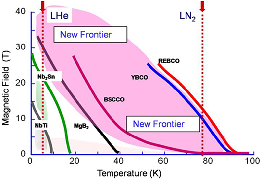
Figure 3. Variation of irreversibility field with temperature for different superconductors including HTS, MgB2, metallic compounds, and alloys. The coated conductor technology including APC methodology has opened new frontiers of superconductivity applications in the temperature range of 5–77 K. Reproduced from Matsumoto and Mele [20], with the permission from IoP Publishing.
The crystal structure of YBCO is a complex variation of the perovskite structure [22], which is shown in Figure 4. As shown in the figure, the YBCO unit cell consists of an YCuO3 cube with adjacent BaCuO3 cubes above and below, but with some oxygen sites not occupied. The oxygen sites on the same horizontal plane as the Y atom are never occupied, which causes the oxygen atoms to move slightly toward the Y atom. The orthorhombic phase of YBa2Cu3O7−δ has lattice parameters, a = 0.382 nm, b = 0.388 nm, and c = 1.168 nm when δ is very small. The oxygen content in YBCO determines its crystal structure and the hole concentration in CuO2 planes. For δ = 1, the compound (YBa2Cu3O6) has the tetragonal structure and it is an insulator. Increasing the oxygen content up to δ = 0.4, the compound undergoes a phase transition from tetragonal to orthorhombic and the Y-Ba-Cu-O system becomes superconducting. Tc approaches its maximum value of 92 K for δ ≈ 0.06 [23] which is ascribed to the optimum hole doping. For δ < 0.06, Tc is found to decrease which is attributed to the overdoped state of the phase in which the concentration of the holes in CuO2 planes exceed the optimum limit. The formation of tetragonal phase is observed in the temperature range of 700–900°C and the orthorhombic phase is formed when the tetragonal phase is slowly cooled in an oxygen atmosphere at ≈ 550°C. The transition from tetragonal to orthorhombic phase creates a large number of different twin domains because of the release of stress in the material. In the tetragonal phase, the oxygen atoms randomly occupy about half of their respective sites in the basal planes whereas they are ordered along the b-direction into Cu-O chains in the orthorhombic phase. This creates oxygen vacancies along the a-direction in the orthorhombic phase which subsequently leads to slight compression of the unit cell so that a < b. The contribution to superconductivity comes both from the CuO2 planes and CuO chains in the orthorhombic phase.
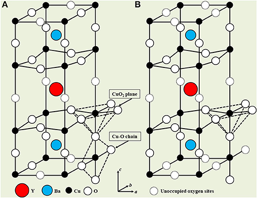
Figure 4. The crystal structure of YBa2Cu3O7−δ for (A) δ = 0 (YBa2Cu3O7) when all of the oxygen sites in the basal planes along the b-direction are occupied and for (B) δ = 1 (YBa2Cu3O6) when all these sites are unoccupied. The intermediate oxygen contents are achieved as these sites are partially occupied when the sample is annealed in oxygen atmosphere. The crystal structure is tetragonal for δ ≥ 0.6 and orthorhombic for δ < 0.6.
As shown in Figure 4, the crystal structure of YBCO is highly anisotropic. This anisotropy is observed in other superconducting properties also, such as energy gap (Δ), coherence length (ξ), and penetration depth (λ). The electrical conduction in YBCO, like other HTS cuprate superconductors, is also highly anisotropic with conductivity along the ab-plane being much higher than along the c-axis [24, 25]. The transport of electrical currents is conducted by holes induced in the oxygen sites of the CuO2 planes. The oxygen occupancy at the chain site influences the carrier density in the CuO2 planes and subsequently the macroscopic electronic properties of YBCO superconductor.
The anisotropic character of YBCO is observed in its characteristics both in normal and superconductive states. The properties along the ab-plane, parallel to the layers, are very different compared to along the c-axis, which is normal to the layers. Apart from other superconducting properties, Jc also exhibits strong anisotropy being higher when the applied magnetic field is oriented along the ab-plane and minimum when the applied magnetic field is oriented along the c-axis of the superconducting sample.
Superconductivity in YBCO was discovered in its polycrystalline bulk sample. Although it has Tc ~ 92 K and relatively large Hirr (~ 7 T at 77 K) in its bulk polycrystalline form, the values of Jc were observed to be ~ 102 A/cm2 (77 K, self-field) [26, 27], which is not high enough as compared to metallic copper. Such a low value of Jc was attributed to low coherence length of YBCO, which results in limited percolation of electrical current across grain boundaries [28]. The alignment of the grains in bulk YBCO and REBCO materials was improved by melt-texturing-growth (MTG) technique [29]. This new approach resulted in much higher Jc ~ 104 A/cm2 (77 K, self-field), two orders of magnitude larger than for polycrystalline bulk samples of YBCO. The recent development of infiltration growth technique has resulted in superior Jc performance (~ 105 A/cm2; 77 K, self-field) of YBCO and REBCO melt-textured bulk samples [30–33]. In addition, the MTG REBCO superconductors exhibited superior capacities to trap very high magnetic fields (~16–17 T at 25–30 K) [34, 35] which could be very useful for permanent magnet applications.
Within a couple of years of its discovery in the polycrystalline bulk sample, it became possible to make thin films of YBCO on single crystal substrates such as SrTiO3, Al2O3, MgO, etc. [36]. Highly c-axis oriented YBCO films on single crystals exhibited Jc > 106 A/cm2 (77 K, self-field) which was again two orders of magnitude larger than the MTG YBCO samples. In a recent work, highly oriented YBCO thin films on different single crystal substrates were deposited and the role of the substrate material and thermal contact during the deposition are carefully investigated [37]. Thus, with the combined progress in the material and its processing, the current carrying capability of REBCO superconductors improved significantly. Highly c-axis oriented YBCO films deposited on single-crystal substrates by different techniques such as pulsed laser deposition (PLD) [38], chemical solution deposition (CSD) [39] and metal organic chemical vapor deposition (MOCVD) [40] exhibited high Jc of 1–5 MA/cm2 at 77 K, self-field [41, 42]. The high value of Jc was attributed to various crystal defects which will be discussed in the next section. The distribution and density of such crystal defects, however, is very difficult to control, which is very much needed for in-field enhancement of Jc. The challenge of improving Jc of YBCO thin films under applied magnetic field remained unresolved for almost a decade.
After successful demonstration of high critical current in epitaxial YBCO films on single crystal substrates, it was desired to develop the technique of making these epitaxial films on flexible metal tapes for technological applications. Subsequently, the development of second-generation wires and tapes or so called coated conductors was carried out by ensuring both in-plane and out-of-plane texturing of REBCO superconducting layers on buffered metal substrates in a biaxial alignment [43]. In order to address this issue, two approaches were employed: ion beam-assisted deposition (IBAD) [44] and rolling-assisted biaxially textured substrates (RABiTS) [45]. In IBAD technique, biaxially oriented buffer layer on polycrystalline metallic substrate is deposited before the deposition of superconducting film. Although IBAD process provides excellent in-plane texture; it involves high equipment costs and is a time-consuming process. Another approach which has been used for the texturing of metal tapes is inclined substrate deposition (ISD) in which textured film of MgO is deposited by electron beam evaporation [46, 47]. The ISD method provides higher deposition rates as compared to IBAD and is independent of recrystallization properties of the metallic substrates. In RABiTS, biaxial texturing is carried out through cold rolling and recrystallization of metallic substrate (Ni). By continuous development of the fabrication methods involving IBAD, ISD, and RABiTS, it was possible to get high self-field Jc in the coated conductors as well.
The defects which are naturally generated during the growth of a superconducting YBCO and REBCO thin films can act as pinning centers are as follows [8]:
(a) Point defects: Point defects are a kind of imperfection which occur when the crystal structure is disrupted on atomic scale. It can be due to impurities, vacancies or interstitials (missing or extra atoms). When YBCO is doped with rare-earth elements like Nd, Sm, and Eu [48, 49], yttrium and barium atoms sometimes exchange their places which also results in point defects.
(b) Voids: During the deposition of the thin film, the vapors of the material are unable to fill the valleys because of the shadowing effect or its reduced mobility. This causes surface roughness in the thin film. When deposition and crystallization of the film is done in separate steps (ex-situ process), pores and voids may result during the crystallization step due to volumetric changes.
(c) Misfit dislocations: Due to the lattice mismatch between REBCO and the substrate on which it is deposited, strain is developed. But when the strain is more than a limit, dislocations are generated in the form of missing (or extra) half-plane of atoms to relieve the stress.
(d) Precipitates: The growth of secondary phases such as Y2O3 or Ba-Cu-O, due to the deviation of stoichiometry from 1:2:3 cationic ratio, causes the formation of precipitates. Such precipitates also contribute to vortex pinning in REBCO thin films.
(e) Planar defects: The formation of a precipitate of a non-123 phase of YBCO such as the copper rich 124 phase leads to the generation of planar defects. The layered structure of YBCO is sometimes disrupted by an extra or missing layer of, for example, CuO2 planes, which results in another kind of planar defect called the stacking fault [50].
(f) Grain boundaries: Grain boundary is one of the most common crystal defects in thin films which separates regions of different orientation of the crystals. The non-uniform growth of the solids during crystallization process results in the formation of grain boundaries. If the angle between the adjacent grain boundaries is small, it is effective for pinning the vortices [51, 52]. However, if the angle between grain boundaries is larger, it results in weak coupling between the adjacent grains and Jc decreases rapidly. In all REBCO films, particularly those which are deposited on coated-conductor substrates that inherently have imperfect crystalline structures, the alignment of a- and b-axes deviates. At the boundaries, where misaligned grains meet, atomic order is disrupted resulting in strain and dislocations which provide pinning to the vortices.
(g) Twin boundaries: The crystal structure of REBCO materials, in their superconducting state, is orthorhombic. During the deposition of REBCO films on crystalline substrates, when c-axis of the material grows perpendicular to the substrate, domains with perpendicular a- and b-axes orientations form. The boundaries where these domains meet are called twin boundaries, which are also a kind of planar defect [53, 54].
(h) Antiphase boundaries: YBCO has a layered structure in which appropriately oxygenated yttrium, barium and copper layers are arranged in a particular order. During the process of growth of the film, domains coalesce with the layers matching yttrium-to-yttrium, barium-to-barium, and copper-to-copper. Sometimes, however, this sequence is disrupted and a boundary between imperfectly matched domains is generated which is called an antiphase boundary [55].
(i) Threading dislocations: During the growth of the film, the dislocations between misoriented grains may also grow simultaneously and run entirely through the film thickness. Sometimes, dislocations form between the growth islands due to lattice mismatch between the substrate and REBCO phase [56, 57].
It has been discussed earlier that the immobilization of vortices is required to achieve high Jc in the presence of large magnetic field. Due to the presence of naturally occurring defects which are described in the previous section, the vortices are pinned in REBCO films. However, the pinning efficiency of these naturally occurring defects against thermal fluctuations is not sufficient to sustain necessary level of Jc at high applied magnetic fields [58, 59]. It has been, therefore, a subject of great interest to improve the Jc values of YBCO and REBCO thin films by introducing additional defects into the superconducting matrix.
There are many methods which have been applied to introduce APCs into YBCO and REBCO superconductors. These can be classified into three main categories:
Different rare-earths in REBCO have different ionic-radii and the effect of ionic-radii on the Tc of REBCO superconductors has been reported in an earlier study [60]. It has been observed that the Tc varies linearly with the ionic-radius of RE ions which was attributed to the strain-induced charge redistribution between the charge reservoir (CuO-chains) and the CuO2 planes. The doping of Ho in YBCO melt-textured samples was conducted and significant enhancement in the in-field Jc was observed in the Ho-doped samples [61]. In order to improve the vortex pinning properties of YBCO superconducting thin films, several rare-earth elements such as Sm, Eu, Nd have been doped in place of Y with different molar cationic ratio [62]. Figure 5 shows the enhanced in-field Jc by up to a factor of 3 as observed in Y2/3Sm1/3Ba2Cu3O7−δ films deposited by PLD technique on single crystal substrates. The enhanced in-field Jc in the doped films has been attributed to the additional random defects and tilted linear defects present in the doped sample. However, the enhanced field-dependent Jc behavior of YxRE1−xBCO compounds as compared to that of YBCO is not very clearly understood.
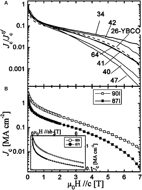
Figure 5. Variation of Jc with applied magnetic field at 75.5 K for REBCO thin films of various rare-earth combinations in (RE1:RE2:RE3)1Ba2Cu3O7−x. (A) Normalized Jc vs. applied field when applied field is along the c-axis. While sample number 26 refers to pristine YBCO, sample numbers 34, 40, 41, 42, 47, and 64 have RE1:RE2:RE3 ratios as (Y:Sm = 1:0.5), (Y:Sm:Nd = 1:0.11:0.05), (Er:Eu = 1:0.24), (Y:Eu:Sm = 1:0.2:0.2), (Dy:Eu:Nd = 1:0.2:0.1), and (Dy:Gd:Sm = 1:0.25:1), respectively. (B) Actual Jc vs. applied field when applied field is along the c-axis for YSmBCO (Y:Sm = 1:0.5) on IBAD-MgO (sample 90I) and YBCO on IBAD-MgO (sample 87I). In the inset of (B), variation of Jc vs. applied field parallel to ab-plane is shown. Reprinted from MacManus-Driscoll et al. [62], with the permission of AIP Publishing.
According to some reports [63–66], in Y-Ba-Cu-O compound, the Y atom is completely replaced by another rare-earth atom or combination of 2 or more rare-earth atoms, which resulted in improved vortex pinning. In order to see if there is additional enhancement resulting from the strain induced by lattice mismatch when mixtures of rare-earth elements were used instead of a single rare-earth element, various combinations were reported which include (Gd0.8Er0.2) [65] and (Nd1/3Gd1/3Eu1/3) [66]. However, in all cases, the enhancement was not remarkable except for the case when the defects were present randomly and not correlated.
Several other elements (Tb, Ce, Pr, Nd, La, Co, Dy, and Eu) have been attempted for substitution at the Y site of YBCO and RE site of REBCO [49, 67–70] films. These substitutions resulted in enhanced Jc and Fp values over a broad range of applied magnetic fields, which was attributed to increased density of nanoprecipitates of these substituents in doped REBCO films as compared to pristine REBCO film which subsequently resulted in stress field due to lattice mismatch between the phases in the resulting REBCO films.
Another way of introducing APCs into REBCO superconductors is the incorporation of nanoscale non-superconducting secondary phase materials into the superconducting matrix. There are several reports in the recent past in which the vortex pinning properties of REBCO superconductors has been improved by intentionally adding non-superconducting secondary phase nanoparticles. Incorporation of different secondary phases such as Al2O3 [71], TiO2 [72], WO3 [73], BaTiO3 [74], BaZrO3 [75, 76] etc. into YBCO polycrystalline bulk samples have been reported in the past which resulted in the enhancement of in-field Jc of YBCO bulk samples. The melt-textured bulk samples of REBCO superconductors consisting of precipitates of secondary phases such as (RE)2BaCuO5 (RE-211) [77, 78], NbO3, MoO3 [79] etc. have also exhibited superior vortex pinning properties resulting in enhanced in-field Jc and Hirr values.
The incorporation of BaZrO3 (BZO) nanostructures into YBCO thin films was reported in an earlier study [80] in which a composite (premixed YBCO:BZO) ablation target was used in the PLD technique. It was found that although BZO nanoinclusions were distributed randomly throughout the YBCO matrix, it produced a significant c-axis correlated enhancement of Jc. In another report [81], yttria-stabilized zirconia (YSZ) was added to the YBCO target, which led to the formation of BZO nanostructures in the as deposited YBCO thin film, presumably leaving a Ba-deficient YBCO film matrix. In this composite film, a self-assembly of vertical arrays of BZO phase was observed. These vertical arrays of self-assembled BZO phase were supposed to arise from the preferential nucleation of the impurity islands in the strain field above the impurity particles [82]. These self-assembled vertical arrays of BZO phase resulted in strong pinning of vortices especially when the applied magnetic field is along the c-axis. Goyal et al. [83] have also reported a strong c-axis correlated pinning enhancement in YBCO:BZO nanocomposite thin films on RABiTS.
The incorporation of BZO nanoinclusions into YBCO thin films has been conducted in many other studies which include study of temperature dependence of Jc for YBCO and YBCO:BZO thin films [84] and field dependence of the optimum concentration of BZO nanoinclusions for effective pinning of vortices [85]. Figures 6A–C shows the cross-sectional and planar views of the microstructure of YBCO:BZO thin films, deposited on IBAD-MgO templates, with varying concentrations of BZO. The variation of the average spacing between the BZO nanorods and the corresponding matching field (Bφ) with respect to BZO concentration is also shown in Figure 6D. As shown in Figure 7, lower concentrations of BZO nanoinclusions are more effective at 77 K, exhibiting higher Fpmax values. However, at 65 K and higher magnetic field, the performance of the YBCO:BZO films with higher concentration of BZO nanoinclusions is enhanced as compared to YBCO:BZO films with low BZO content.
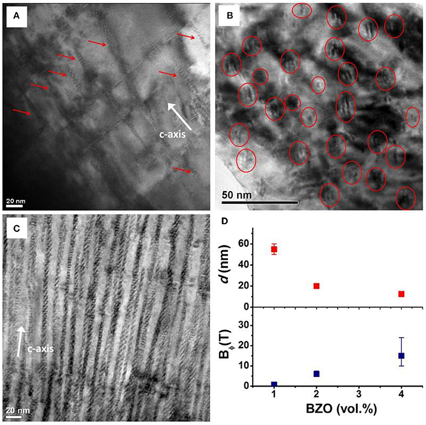
Figure 6. Cross-sectional TEM images of (A) YBCO:BZO 1 vol% and (C) YBCO:BZO 4 vol% thin films. (B) Plan-view TEM image YBCO:BZO 2 vol% thin film. (D) The variation of average BZO nanocolumn spacing, d, and corresponding matching field, Bφ, with BZO concentration. Reproduced from Wee et al. [85].
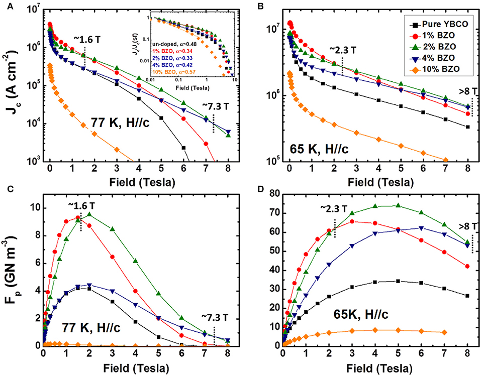
Figure 7. Variation of Jc and Fp for pristine YBCO and YBCO:BZO thin films with varying concentration of BZO (1–10 vol%) at 77 K (A,C) and 65 K (B,D). The inset of (A) shows normalized Jc, Jc(H)/Jc(sf), for all the studied thin film samples. Reproduced from Wee et al. [85].
The CSD method has also been employed to prepare YBCO:BZO nanocomposite thin films which exhibited strongly enhanced vortex pinning [86]. Unlike the previous results in which films were deposited using PLD technique, the solution process was found to produce non-epitaxial secondary phase particles in the film matrix surrounded by many crystalline defects. Figure 8 shows the microstructure of the YBCO:BZO nanocomposite thin film using transmission electron microscopy (TEM) in which the separate phase of BZO nanoparticles and crystalline defects surrounding them can be clearly observed. The formation of BZO nanoparticles inside YBCO matrix resulted in isotropic pinning characteristics of these films [87, 88]. The significant improvement in the value of Jc and Fp of the YBCO:BZO nanocomposite thin films can be seen in Figure 9.
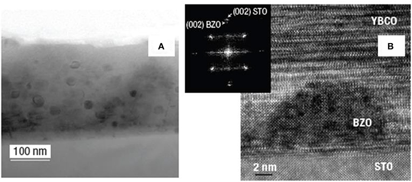
Figure 8. (A) Cross-sectional TEM image of a YBCO:BZO nanocomposite film in which BZO nanoparticles can be clearly observed. (B) High-resolution TEM image of a BZO nanoparticle grown near the interface with the single-crystal substrate. Inset shows the fast Fourier transform of the image in which the epitaxial relationship between BZO and YBCO can be seen in the diffraction peaks. Reprinted from Gutierrez et al. [86], with the permission from Springer Nature© (2007).
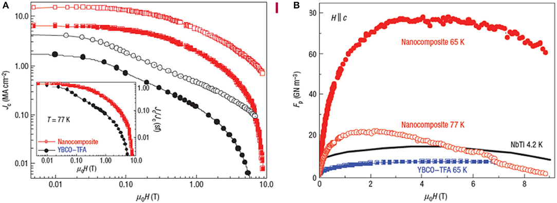
Figure 9. (A) Variation of Jc with applied magnetic field for YBCO:BZO(10%) nanocomposite film (red symbols) and a pristine YBCO sample (black symbols) grown by CSD technique. The solid and hollow symbols correspond to the data measured at 77 and 65 K, respectively. In the inset, variation of the normalized Jc with applied magnetic field at 77 K for pristine and nanocomposite films is shown. (B) Variation of Fp with applied magnetic field for the nanocomposite film at 65 and 77 K in comparison with that of pristine YBCO at 65 K and NbTi wires at 4.2 K. Reprinted from Gutierrez et al. [86], with the permission from Springer Nature© (2007).
By adopting a different approach in PLD technique, Haugan et al. [89] have successfully incorporated a non-superconducting phase, Y2BaCuO5 (Y211), into YBCO thin film in a controlled manner. Two different targets, one of YBCO and another of Y211, were used and by depositing thin YBCO layers and discontinuous Y211 layers alternately, a pancake-like array of precipitates were formed in the resulting film matrix. In this case, enhanced vortex pinning properties was found for both the field orientations: when H was parallel to the c-axis and also for H parallel to the ab-plane [90]. Very recently it was demonstrated that these Y211 nanoparticles are effective not only in increasing the in-field Jc but also in reducing the critical current anisotropy [91].
Apart from BZO and Y211, the nanostructures of other materials such as Y2O3 (YO) [92], BaSnO3 (BSO) [93–95], and BaTiO3 (BTO) [96] have also been successfully incorporated into YBCO thin films using the PLD technique. In all these cases, the enhancement in the value of Jc was more prominent at higher applied magnetic field. In one of the reports [95], the Fpmax value for YBCO:BSO nanocomposite film turned out to be 28.3 GNm−3, a record of that time, which reflects the excellent in-field performance of Jc. The incorporation of a double-perovskite material, YBa2NbO6 (YBNO), was also reported and it was found that YBNO phase grows in the form of columnar nanostructures [97]. In another report, the YBNO nanocolumns were introduced into YBCO thin films by surface modified target method in which YBNO concentration inside YBCO thin film was controlled by controlling the target rotation speed [98]. YBNO nanocolumns were observed to be very effective in enhancing the in-field Jc of YBCO thin films. Rare-earth tantalates (RE3TaO7, REBa2TaO6) also turned out to be excellent secondary phase materials which were incorporated inside REBCO superconducting matrix for enhancing in-field Jc of REBCO thin films [99, 100]. It has been suggested that the lattice mismatch is appropriate for superior vortex pining if it is in the range of 5–12% [100].
The nanoinclusions of the rare-earth tantalate and niobate have simultaneously been incorporated into YBCO thin films which significantly enhanced the Jc of YBCO films and improved the angular anisotropy of Jc [101]. Extremely high Fpmax values have been observed in YBCO films with YBa2(Nb/Ta)O6 (YBNTO) nanoinclusions [102]. Figure 10 shows the microstructure of the YBCO film with YBNTO nanoinclusions. Apart from YBNTO nanocolumns, other pinning centers such as Y2O3 nanoparticles and planar defects can also be observed in this figure. Figure 11 shows the variation of Jc and Fp, at 77 K and 30 K, for YBCO films with YBNTO nanoinclusions deposited at different frequencies in the PLD system. At 77 K, Fpmax exceeded 25 GNm−3 and at 30 K, it exceeded 300 GNm−3 which can be seen as excellent in-field Jc performance of these YBCO nanocomposite thin films.
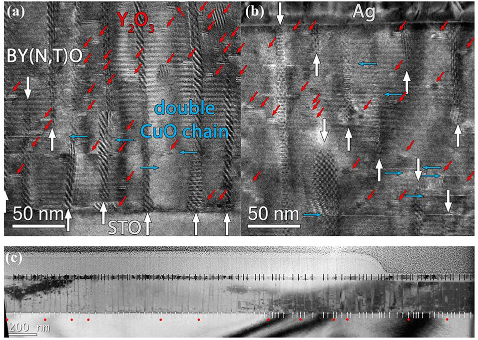
Figure 10. High-resolution TEM images of YBCO:YBNTO (YBCO + 2.5 mol% BYNO + 2.5 mol% BYTO) thin films, deposited at 1 Hz, near substrate-film interface (a) and near the film surface (b). Different pinning centers such as YBNTO nanocolumns, Y2O3 nanoparticles and planar defects are marked. (c) Bright-field TEM cross-sectional image of the 1 Hz sample over larger width (3,200 nm). YBNTO nanocolumns are marked with arrows. The nanocolumns which are tilted are marked by red dots. Reproduced from Opherden et al. [102].
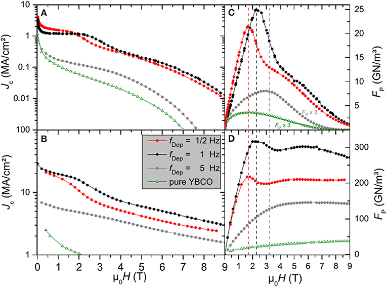
Figure 11. Variation of Jc and Fp with applied magnetic field for YBCO:YBNTO (YBCO + 2.5 mol% YBNO + 2.5 mol% YBTO) thin films, deposited at different frequencies, at 77 K (A,C) and 30 K (B,D). Reproduced from Opherden et al. [102].
More recently BaHfO3 (BHO) has emerged out as a very promising secondary phase material whose nanoinclusions in the form of columnar or spherical structures inside REBCO matrix resulted in significantly enhanced in-field Jc of REBCO thin films deposited on both single crystals and metallic tapes [103–110]. By adopting low-temperature growth technique in PLD, SmBCO:BHO films have been demonstrated to exhibit very high pinning force density (Fpmax = 28 GN/m3) at 77 K for H parallel to the c-axis [107]. Even on metallic tapes, GdBCO:BHO nanocomposite films exhibited large values of pinning force density (Fpmax = 23.5 GN/m3) and irreversibility field (μ0Hirr = 15.8 T) at 77 K for H parallel to the c-axis [108]. The CSD approach has also been employed to incorporate BHO nanoparticles into YBCO [109] and GdBCO [110] thin films, which resulted in the enhanced in-field Jc values of the nanocomposite thin films.
By adopting a different synthesis route called MOCVD, researchers at University of Houston in USA have demonstrated that the incorporation of BZO in high volume fractions results in outstanding in-field Jc performance of REBCO films which are relatively thicker (~ 1–2 μm) [111–116]. The Fpmax value of one of these composite films reached a record value of 1.7 TN/m3 at 4.2 K together with extremely high μ0Hirr ~ 14.8 T (at 77 K), a value that is much higher than the μ0Hirr ~ 11 T of NbTi superconductor at 4.2 K [111]. Figure 12 shows the cross-sectional TEM image of a heavily doped (Gd,Y)BCO superconducting film on IBAD substrate prepared by MOCVD technique in which c-axis oriented self-assembled BZO nanocolumns can be clearly observed. Figure 13 shows the variation of Jc and Fp with respect to applied magnetic field for the films with different concentration of Zr inclusions (in mol %). It can be observed that in heavily doped film, Fpmax exceed the value of 1 TNm−3 which is excellent in terms of critical current performance.
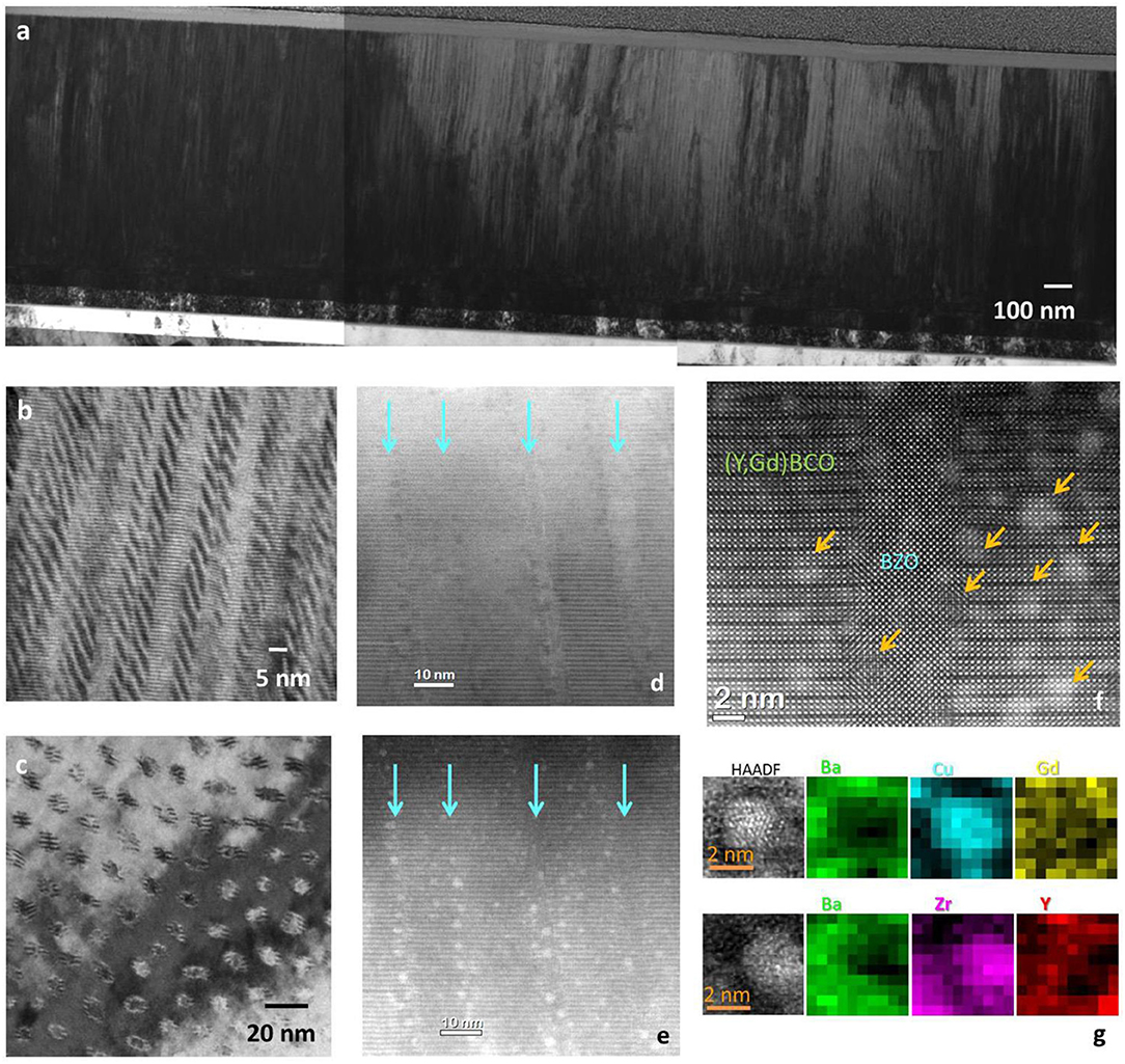
Figure 12. Cross-sectional TEM image of a (Gd, Y)BCO film with 25 mol% Zr on IBAD grown by MOCVD technique. (a,b) Show that BZO nanocolumns are formed which are about 5 nm in diameter and aligned along the crystallographic c-direction. Planar view of the microstructure is shown in (c), whereas (d–f) show the bright-field image, high angle annular dark field image and high-resolution cross-sectional image. The compositional map of a nanoparticle is conducted by electron energy loss spectrometer and is shown in (g). Reprinted from Selvamanickam et al. [113], with the permission of AIP Publishing.
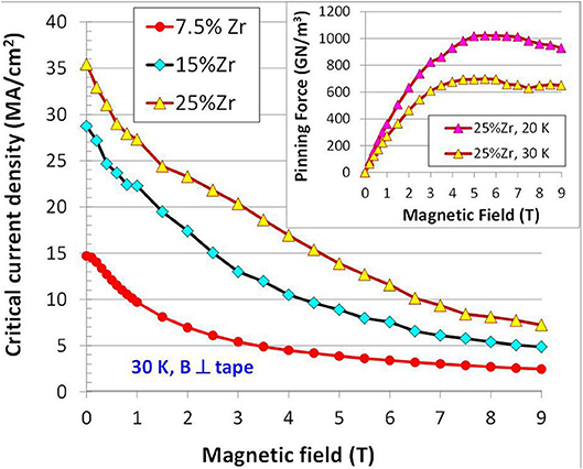
Figure 13. Variation of critical current density with applied magnetic field for 7.5, 15, and 25 mol.% Zr-added (Gd,Y)BCO superconductor tapes at 30 K for H perpendicular to the tape. Variation of pinning force density of 25 mol.% Zr-added (Gd,Y)BCO superconductor tape at 30 and 20 K is shown in the inset. Reprinted from Selvamanickam et al. [113], with the permission of AIP Publishing.
The so-called quasi-multilayer (multilayers in which layer/s of one phase is incomplete) approach has also been employed for improving vortex pinning in YBCO thin films. The quasi-multilayers of YBCO with different materials such as Y2O3 [117, 118], BZO [119], and transition metals such as Ir [120] and Ti, Zr, Hf [121] and prepared by PLD technique have been investigated. The transition metals when incorporated into YBCO thin films, through this approach, have been observed to form BaMO3 (M = Ti, Zr, Hf, Ir) phase. Not only enhancement in the in-field Jc of YBCO based quasi-multilayers was observed, but the irreversibility line was also observed to shift toward higher H-T regime [119].
The materials, whose precipitates or nanoparticles have been mentioned so far, for their use as secondary phase inclusions in the YBCO/REBCO thin films, are mostly insulating and non-magnetic in nature. However, there have been successful attempts of using ferromagnetic secondary phase inclusions as a source of APCs in YBCO thin films. A thin layer of Fe2O3 has been used either as a cap layer on YBCO thin film or as a buffer layer on STO substrate before YBCO film deposition [122, 123]. It has been observed that the samples consisting of Fe2O3 cap layer have exhibited significant enhancement in the Jc (both self-field and in-field) of YBCO thin films. In addition, other ferromagnetic nanoinclusions such as of YFe3O4 [124] and CoFe2O4 [125] have also been successfully used to enhance the vortex pinning properties of YBCO thin films. The incorporation of Fe into the YBCO matrix at sufficiently low concentrations was effective for vortex pinning and the so-called “poisoning effect” was observed as its concentration is increased [126]. The enhanced vortex pinning properties of the YBCO films with ferromagnetic nanoinclusions have been discussed in terms of Lorentz force reduction pinning mechanism which is effective for low field regime (up to ~ 1 T) [127]. It has been suggested that in the low field regime, the magnetic flux is effectively reduced from the vortices which subsequently reduces the Lorentz force on the vortex lattice.
On the basis of numerous experimental results, it became apparent that some of the secondary phase nanoinclusions tend to self-assemble in the form of nanocolumns along the c-axis direction, while others become nanoparticles with different sizes. The self-assembled columnar nanostructures of perovskite and double-perovskite materials such as BSO, BZO, BSO, YBNO etc. are very effective in enhancing Jc particularly when the applied magnetic field is normal to the film surface. However, at higher temperatures, the vortices tend to form double kink structures under the influence of thermal excitations. Even if the matrix contains c-axis correlated defects (nanocolumns), the unpinned vortex segments can move due to the acting Lorentz force. Moreover, as applied magnetic field direction changes from normal to the film surface toward ab-plane, the columnar nanostructures start losing the vortex segments gradually and at enough inclination these vortices become free from the columnar pinning sites. Such a situation is represented in Figure 14. It was, therefore, considered to incorporate mixed pinning landscapes in the REBCO films so that vortices may remain pinned even if the applied magnetic field is tilted from the c-axis of the films. This would result in increased Jc in the intermediate angular regime (between ab-plane and c-axis), and the angular anisotropy of the critical current density would thus be reduced.
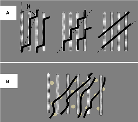
Figure 14. Schematic illustration of (A) possible vortex configurations for varying inclinations of applied magnetic field (θ) with respect to the columnar disorders aligned along the c-axis of the YBCO films and (B) pinning of vortices provided by spherical nanoparticles located randomly between the columnar disorders in the YBCO matrix. Reproduced from Jha et al. [131], with the permission from IoP Publishing.
The use of two different kinds of pinning landscapes was reported by Mele et al. [128] in which BZO nanocolumns and YO nanoparticles were simultaneously incorporated into YBCO film deposited by PLD technique. Although, Jc was increased slightly in the intermediate angular regime, but it was found to decrease along the c-axis of the film as compared to BZO added YBCO film (columnar pins only). Later, the combinations of nanocolumns and nanoparticles of different materials have also been reported where the in-field Jc was enhanced and anisotropy of Jc of YBCO thin films was sufficiently reduced [129–132]. The use of BSO nanocolumns together with YO nanoparticles was attempted on metallic tape as well and significant enhancement of in-field Jc and reduction in Jc anisotropy was reported [133]. The combination of BSO nanocolumns and Y2O3 (YO) nanoparticles as hybrid APCs was very effective in controlling the angular anisotropy of the Jc of YBCO thin films [130]. The cross-sectional TEM images of YBCO+BSO3% and YBCO+BSO3%+YO nanocomposite films are shown in Figure 15 in which formation of only columnar nanostructures in YBCO+BSO thin film and that of both columnar and spherical nanostructures in YBCO+BSO+YO thin film can be clearly observed. Figure 16 shows the angular variation of Jc measured at 77 K, 1 T and 65 K, 3 T for pristine YBCO, YBCO+BSO, and YBCO+BSO+YO thin films. The superior in-field Jc performance with reduced anisotropy for YBCO thin films consisting of hybrid APCs can be clearly observed in Figure 16.
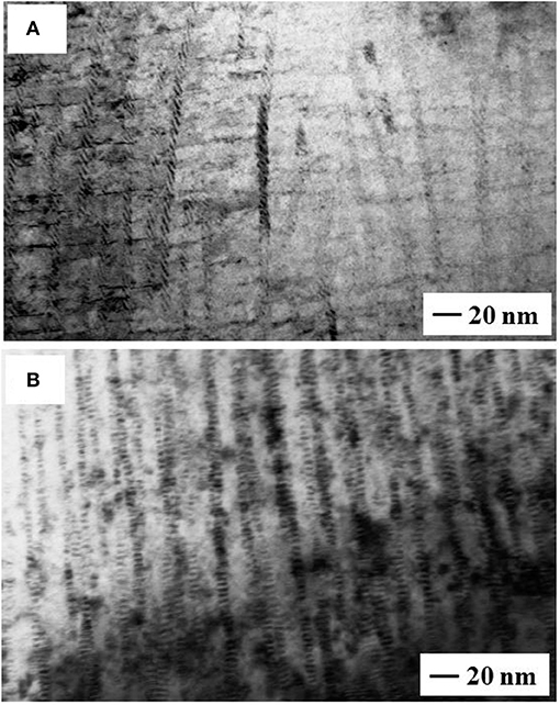
Figure 15. Cross-sectional TEM images of YBCO films with (A) BSO nanocolumns and (B) BSO nanocolumns and Y2O3 nanoparticles deposited by surface modified target method. Reproduced from Jha et al. [130], with the permission from IEEE Publishing.
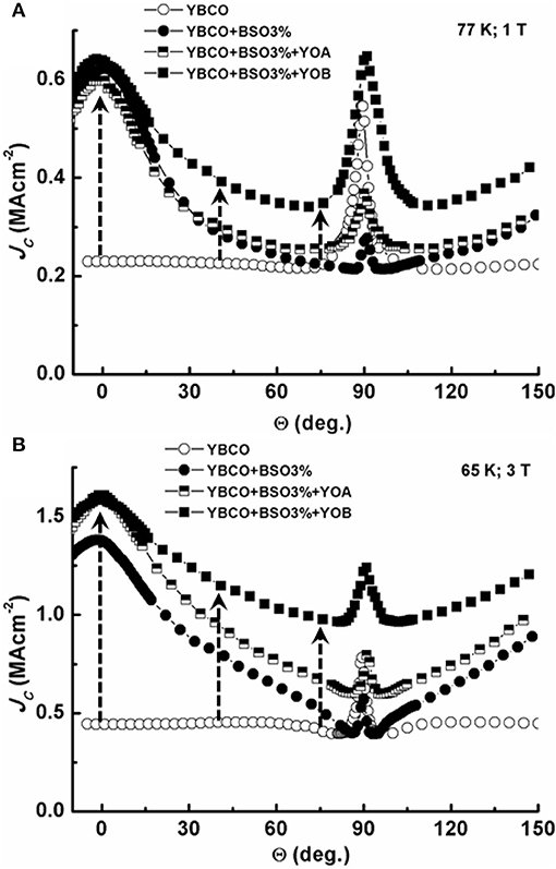
Figure 16. Angular variation of Jc for pristine YBCO, YBCO+BSO, and YBCO+BSO+Y2O3 nanocomposite films measured at (A) 77 K, 1 T, and (B) 65 K, 3 T. Two different Y2O3 pieces, 2.2 area and 3 area%, are referred as YOA and YOB, respectively. Reproduced from Jha et al. [130], with the permission from IEEE Publishing.
Successful incorporations of different combinations of nanocolumns and nanoparticles into YBCO thin films were later reported in which BSO nanocolumns and Y211 nanoparticles [132], BZO nanocolumns and BaCeO3 nanoparticles [134], and BHO nanocolumns and YO nanoparticles [135] were simultaneously incorporated into YBCO thin films, which resulted in superior in-field Jc performance with reduced anisotropy. Hybrid APCs were also incorporated in the form of segmented BSO nanocolumns [136] and segmented nanocolumns with YO nanoparticles [137].
From an energetics point of view, a pinned vortex line is more stable than a free vortex in a superconductor. For a non-superconducting particle, the energy gain by a vortex line per unit of interaction volume equals to the condensation energy in the core region. The total pinning energy for a vortex line is, therefore, given by [138]:
where, is the thermodynamic critical field, Φ0 is the flux quantum, ξab and λab are the coherence length and the penetration depth along the ab-plane and d the size of the non-superconducting inclusion. where, γ (= 5–7) is the electronic mass anisotropy parameter. When the vortex line is pinned at the normal core, energy has to be spent to move it away from the core. The force needed to eject a vortex line segment is called the elementary pinning force and is related to the condensation energy as follows:
Considering each vortex is individually pinned by a non-superconducting core region, and the elastic energies are considerably smaller than the pinning energies, the global pinning force per unit volume may be given by directly summing the elementary pinning forces over all the pinning sites [138].
where N is the density of non-superconducting precipitates, and dp and a0 are the average separation among the pinning centers and flux lines, respectively. According to this equation, the global pinning force is directly proportional to the concentration of pinning centers. It is, however, to be noted that the nature of Equation (4) is simplistic in the sense that it assumes that all the pinning centers are of equal strength. The density of APCs, however, has an upper limit also for being efficient enough for vortex pinning before the superconductive matrix is severely degraded. Gurevich [139] and other researchers [140, 141] considered nanoparticles of materials such as YO or Y211 as strong pinning centers where parts of the vortex segments can be pinned strongly. If a vortex segment is pinned by two non-superconducting nanoparticles separated by a distance d, then the expression for the upper limit of critical current density, according to their model, is given by:
where the terms have their usual meanings. As per this equation, the Jc value is proportional to the term and for smaller separation among the nanoparticles (higher the concentration), higher Jc is anticipated. However, too much incorporation of such non-superconducting nanoparticles may result in the degradation of the superconducting matrix and hinder the transport of electrical current leading to low Jc [142].
In order to improve vortex pinning in REBCO superconductive films, the inclusion of nanoscale secondary phases remains the most extensively studied among all the techniques. These nanoscale inclusions are considered as strong pinning centers and are very effective depending upon their density and geometry/morphology within the superconducting matrix [8]. It is, however, very interesting to observe that these secondary phase nanoinclusions have different morphologies within the REBCO matrix and accordingly they are efficient for different range of H orientations. While columnar nanostructures are effective for H oriented along the c-axis (exhibiting a strong Jc peak for H//c-axis), spherical nanoparticles are observed to be effective for larger angular range of H. It, therefore, becomes imperative to understand the physical origin of varying morphology of these nanoscale inclusions. One of the fundamental parameters which decides the geometry of these nanoscale structures within REBCO thin films, is the lattice mismatch between the two phases. Apart from the lattice mismatch, the surface diffusion of adatoms also play a crucial role in determining the interface between the two phases, which may be coherent, semi-coherent or non-coherent [86]. While the surface energies of coherent and semi-coherent interfaces are much lower, that of the non-coherent interfaces are much higher which results in the observation of many phenomena such as coarsening of the grains in polycrystalline films [143] and faceting of precipitates and grain boundaries [144].
In recent years, Wu et al. in a series of reports [11, 145–149], have attempted to explain the morphology of the nanoinclusions on the basis of elastic strain model. They have found that the APC morphology is determined by the combined effect of the lattice mismatch and elastic properties of REBCO and secondary phase materials. Based on their calculations, they defined a phase boundary separating two regions: c-axis aligned columnar nanostructures are preferred energetically on one side of the boundary and not preferred on the other side of the boundary. Their calculations were in good agreement with experimentally obtained results on well-aligned nanocolumns of materials such as BZO [83, 150], BSO [94], BHO [103, 151, 152], and YBNO [97] and spherical nanoparticles of other materials such as Y211 [153] and YO [154, 155] which are on the other side of the calculated phase boundary.
Substrate surface modification is one of the earliest methods used to introduce APCs into superconducting thin film to improve its vortex pinning characteristics. This method provides a means for generating nanostructured APCs by decoration of the substrate surface by non-superconducting secondary phase nanoparticles which generates interfacial defects between the phases. Before the deposition of superconducting thin film, the decoration of the substrate surface is accomplished by growing nanoparticles of various species such as metals [156, 157] or oxides [158–164] on the substrate. The substrate surface is modified by processing an oxide layer in such a way that nanoscale outgrowth develops naturally on the deposition surface. Due to the presence of these nanoparticles at the substrate/film interface, the lattice planes of YBCO are distorted or buckled above the nanoparticles, resulting in low-angle grain boundaries or dislocations that may extend through the entire thickness of the thin film. Matsumoto et al. [159] have reported that the presence of YO nanoparticles at the substrate/film interface produced c-axis-correlated pinning which was reflected in the enhancement of Jc when H was parallel to the c-axis. In another report by Aytug et al. [157], where STO is treated with Ir nanoparticles, the enhancement in Jc was observed. The authors have shown that the YBCO planes above the grown Ir nanoparticles are buckled and give rise to random pinning. Random pinning, generally, is caused by the homogeneous distribution of the point defects throughout the film volume. Since in this case the film thickness is 100–200 nm, the presence of strain fields through the entire thickness is supposed to create the appearance of a volumetric particle distribution. The difference in the pinning mechanism due to YO and Ir nanoparticles can be understood in terms of their chemical reaction with the YBCO phase. In the case when Ir is present at STO/YBCO interface, these Ir nanoparticles might have reacted partially with YBCO and the volumetric change that could have taken place might have provided an alternate way to relieve the strain thereby reducing the driving force for dislocation formation and eliminating correlated pinning enhancement. But, YO nanoparticles are chemically inert with YBCO, and therefore, these are intact at the substrate/film interface. Later, ferromagnetic La0.7Sr0.3MnO3 (LSMO) nanoparticles were also successfully grown on the STO surface by PLD technique before the growth of YBCO thin film [165]. Figure 17 shows the atomic force microscope (AFM) images of undecorated and LSMO nanoparticle decorated STO substrates onto which YBCO thin films were deposited. The decorated sample exhibited enhanced in-field Jc than the undecorated sample which can be observed in Figure 18. It was suggested in this report that the presence of LSMO nanoparticles at the YBCO/STO interface could generate structural defects such as threading dislocations which would result in c-axis vortex pinning in the resulting YBCO film. The enhanced Jc values for the YBCO film on decorated substrate can also be understood in terms of Lorentz force reduction pinning mechanism [127]. In such a scenario, the Lorentz force splits between the vortices and the magnetic pinning sites which results in higher current density before the vortices start depinning from the defects. The metal organic decomposition method has also been employed for decoration of the substrate surface for improving the vortex pinning properties of YBCO thin films [166–168].
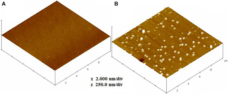
Figure 17. Atomic force micrograph of STO substrates (A) without decoration and (B) decorated with LSMO nanoparticles. The random distribution of LSMO nanoparticles on the STO substrate surface can be clearly observed in Figure (B). Reproduced from Jha et al. [165], with the permission from AIP Publishing.
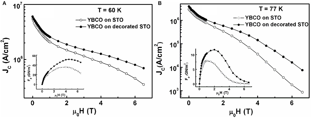
Figure 18. Variation of critical current density with applied magnetic field as measured at (A) 60 K and (B) 77 K for YBCO films on the undecorated and LSMO decorated STO substrates. Variation of the corresponding pinning force density with applied magnetic field is shown in the insets of (A,B). Reproduced from Jha et al. [165], with the permission from AIP Publishing.
REBCO superconductors are the most promising HTS for their high Tc and Jc values. However, for their use in several applications in the practical range of temperature and applied magnetic field, pinning of vortices is an essential requirement. It has been shown that the defects that are generated naturally during the growth of the sample (bulk or thin film) are not sufficient to pin the vortices at elevated temperatures and applied magnetic fields. That is how the need of introducing artificial pinning centers arose and extensive work has been carried out to address this issue.
In recent years, a variety of methods have been reported to intentionally introduce nanostructured defects into the REBCO superconducting samples which include doping of rare-earth elements, addition of secondary phase nanostructures and modification of the substrate surface. The different methods for introducing artificial pinning centers lead to different and interesting underlying physics. The dominant pinning mechanism needs to be investigated which governs the role of artificial pinning centers in these superconducting samples.
The various interesting issues and future potential applications based on REBCO superconducting films have provoked researchers to continue activities in this field of research. The generation of nanoscale APCs with desired density, geometry and orientation is very much needed for vortex pinning in REBCO nanocomposite films deposited on single crystals and metallic tapes. Precise control of these parameters is very promising for optimal pinning of the vortices as required to push the limits of critical current performance.
AJ conceived the idea of highlighting the role of rare-earth oxides in promoting sustainable energies. AJ and KM discussed the development in this area over the years and contributed to the manuscript.
The authors declare that the research was conducted in the absence of any commercial or financial relationships that could be construed as a potential conflict of interest.
We would like to thank N. Khare, T. Horide, P. Mele, S. Saini, A. Ichinose, R. Pinto, Y. Yoshida, and S. Awaji for cooperative research on vortex pinning studies in YBCO nanocomposite films. This work is supported by the research startup grant provided by Kyushu Institute of Technology. Partial financial support from ALCA project of the Japan Science and Technology Agency is also thankfully acknowledged.
1. Onnes HK. Further experiments with liquid helium. On the change of electric resistance of pure metals at very low temperatures etc. The resistance of pure mercury at helium temperatures. (i)Leiden Comm. 120b, reprinted in Proceedings of the Koninklijke Nederlandse Akademie van Wetenschappen. (1911). p. 1479–81. (ii)Leiden Comm. 122b, reprinted in Proceedings of the Koninklijke Nederlandse Akademie van Wetenschappen. (1911). p. 81–3. (iii)Leiden Comm.124c, reprinted in Proceedings of the Koninklijke Nederlandse Akademie van Wetenschappen. (1911). p. 799–802.
2. Meissner W, Ochsenfeld R. Ein neuer Effekt bei Eintritt der Supraleitfähigkeit. Naturwissenschaften. (1933) 21:787–8. doi: 10.1007/BF01504252
3. Poole CPJr, Farach HA, Creswick RJ, Prozorov R. Superconductivity. Amsterdam: Academic Press (2007). p. 61–82.
4. Gottlieb U, Lasjaunias JC, Tholence JL, Laborde O, Thomas O, Madar R. Superconductivity in TaSi2 single crystals. Phys Rev B. (1992) 45:4803–6. doi: 10.1103/PhysRevB.45.4803
5. Ren Z-A, Kato J, Muranaka T, Akimitsu J, Kriener M, Maeno Y. Superconductivity in Boron-doped SiC. J Phys Soc Jpn. (2007) 76:103710. doi: 10.1143/JPSJ.76.103710
6. Larbalestier D, Gurevich A, Feldmann DM, Polyanskii A. High-Tc superconducting materials for electric power applications. Nature. (2001) 414:368–77. doi: 10.1038/35104654
8. Foltyn SR, Civale L, Macmanus-Driscoll JL, Jia QX, Maiorov B, Wang H, et al. Materials science challenges for high-temperature superconducting wire. Nat Mater. (2007) 6:631–42. doi: 10.1038/nmat1989
9. Kunchur MN. Current-induced pair breaking in magnesium diboride. J Phys Condens Matter. (2004) 16:R1183–R1204. doi: 10.1088/0953-8984/16/39/R01
11. Wu J, Shi J. Interactive modeling-synthesis-characterization approach towards controllable in situ self-assembly of artificial pinning centers in RE-123 films. Supercond Sci Technol. (2017) 30:103002. doi: 10.1088/1361-6668/aa8288
12. Wu MK, Ashburn JR, Torng CT, Hor PH, Meng RL, Gao L, et al. Superconductivity at 93 K in a new mixed-phase Y-Ba-Cu-O compound system at ambient pressure. Phys Rev Lett. (1987) 58:908–10. doi: 10.1103/PhysRevLett.58.908
13. Maeda H, Tanaka Y, Fukutomi M, Asano T. A new high-Tc oxide superconductor without a rare earth element. Jpn J Appl Phys. (1988) 27:L209–L210. doi: 10.1143/JJAP.27.L209
14. Parkin SSP, Lee VY, Engler EM, Nazzal AI, Huang TC, Gorman G, et al. Bulk superconductivity at 125 K in Tl2Ca2Ba2Cu3Ox. Phys Rev Lett. (1988) 60:2539–42. doi: 10.1103/PhysRevLett.60.2539
15. Schilling A, Cantoni M, Guo JD, Ott HR. Superconductivity above 130 K in the Hg–Ba–Ca–Cu–O system. Nature. (1993) 363:56–8. doi: 10.1038/363056a0
16. Gurevich A. To use or not to use cool superconductors? Nat Mater. (2011) 10:255–9. doi: 10.1038/nmat2991
17. Malozemoff AP, Worthington TK, Yeshurun Y, Holtzberg F, Kes PH. Frequency dependence of the ac susceptibility in a Y-Ba-Cu-O crystal: a reinterpretation of Hc2. Phys Rev B. (1988) 38:7203–6. doi: 10.1103/PhysRevB.38.7203
18. Schilling A, Jin R, Guo JD, Ott HR. Irreversibility line of monocrystalline Bi2Sr2CaCu2O8: experimental evidence for a dimensional crossover of the vortex ensemble. Phys Rev Lett. (1993) 71:1899–902. doi: 10.1103/PhysRevLett.71.1899
19. Pastoriza H, Goffman MF, Arribere A, de la Cruz F. First order phase transition at the irreversibility line of Bi2Sr2CaCu2O8+δ. Phys Rev Lett. (1994) 72:2951–4. doi: 10.1103/PhysRevLett.72.2951
20. Matsumoto K, Mele P. Artificial pinning center technology to enhance vortex pinning in YBCO coated conductors. Supercond Sci Technol. (2010) 23:014001. doi: 10.1088/0953-2048/23/1/014001
21. Obradors X, Puig T. Coated conductors for power applications: materials challenges. Supercond Sci Technol. (2014) 27:044003. doi: 10.1088/0953-2048/27/4/044003
22. Cava RJ, Batlogg B, van Dover RB, Murphy DW, Sunshine S, Siegrist T, et al. Bulk superconductivity at 91 K in single-phase oxygen-deficient perovskite Ba2YCu3O9−δ. Phys Rev Lett. (1987) 58:1676–9. doi: 10.1103/PhysRevLett.58.1676
23. Ossandon JG, Thompson JR, Christen DK, Sales BC, Kerchner HR, Thomson JO, et al. Influence of oxygen deficiency on the superconductive properties of grain-aligned YBa2Cu3O7−δ. Phys Rev B. (1992) 45:12534–47. doi: 10.1103/PhysRevB.45.12534
24. Zaanen J, Paxton AT, Japsen O, Anderson OK. Chain-fragment doping, and the phase diagram of YBa2Cu3O7−x. Phys Rev Lett. (1988) 60:2685–8. doi: 10.1103/PhysRevLett.60.2685
26. Babic E, Drobac D, Horvat J, Marohnic Z, Prester M. Inter-, and intragrain critical currents in a dense YBa2Cu3O7 ceramic. Supercond Sci Technol. (1989) 2:164–8. doi: 10.1088/0953-2048/2/3/002
27. Male SE, Chilton J, Caplin AD, Guy CN, Newcomb SB. Critical currents, magnetisation, and network models of polycrystalline YBa2Cu3O7. Supercond Sci Technol. (1989) 2:9–16. doi: 10.1088/0953-2048/2/1/003
28. Dimos D, Chaudhari P, Mannhart J. Superconducting transport properties of grain boundaries in YBa2Cu3O7 bicrystals. Phys Rev B. (1990) 41:4038–49. doi: 10.1103/PhysRevB.41.4038
29. Murakami M. (Ed.) Melt-Processed High-Temperature Superconductors. Singapore: World Scientific (1992).p. 68–100.
30. Muralidhar M, Ide N, Koblischka MR, Diko P, Inoue K, Murakami M. Microstructure, critical current density, and trapped field experiments in IG processed Y-123. Supercond Sci Technol. (2016) 29:054003. doi: 10.1088/0953-2048/29/5/054003
31. Muralidhar M, Kenta N, Zeng XL, Koblischka MR, Diko P, Murakami M. Record critical current densities in IG processed bulk YBa2Cu3Oy fabricated using ball-milled Y2Ba1Cu1O5 phase. Phys Status Solidi A. (2016) 213:443–9. doi: 10.1002/pssa.201532632
32. Das D, Muralidhar M, Ramchandra Rao MS, Murakami M. Top-seeded infiltration growth of (Y, Gd)Ba2Cu3Oy bulk superconductors with high critical current densities. Supercond Sci Technol. (2017) 30:105015. doi: 10.1088/1361-6668/aa83da
33. Naik SPK, Muralidhar M, Jirsa M, Murakami M. Growth, and physical properties of top-seeded infiltration growth processed large grain (Gd, Dy)BCO bulk superconductors. J Appl Phys. (2017) 122:193902. doi: 10.1063/1.4999164
34. Tomita M, Murakami M. High-temperature superconductor bulk magnets that can trap magnetic fields of over 17 tesla at 29 K. Nature. (2003) 421:517–20. doi: 10.1038/nature01350
35. Durrell JH, Dennis AR, Jaroszynski JE, Ainslie MD, Plamer KGB, Shi YH, et al. A trapped field of 17.6 T in melt-processed, bulk Gd-Ba-Cu-O reinforced with shrink-fit steel. Supercond Sci Technol. (2014) 27:082001. doi: 10.1088/0953-2048/27/8/082001
36. Dijkkamp D, Venkatesan T, Wu XD, Shaheen SA, Jisrawi N, Min-Lee YH, et al. Preparation of Y-Ba-Cu oxide superconductor thin films using pulsed laser evaporation from high Tc bulk material. Appl Phys Lett. (1987) 51:619–21. doi: 10.1063/1.98366
37. Huhtinen H, Ulriksson J, Malmivirta M, Jarvinen J, Jha R, Awana VPS, et al. Deposition of YBCO thin films in view of microwave applications. IEEE Trans Appl Supercond. (2017) 27:7501205. doi: 10.1109/TASC.2017.2669484
38. Schey B. Chapter 14: Pulsed Laser Deposition of High-Temperature Superconducting Thin Films and Their Applications. In: Eason R, editor. Pulsed Laser Deposition of Thin Films. Hoboken, NJ: Wiley (2007). p. 313–32.
39. M. Miura Chapter 1: Nanostructured Oxide Superconducting Films Prepared by Metal Organic Deposition. In: Mele P, Endo T, Arisawa S, Li C, Tsuchiya T, editors. Oxide Thin Films, Multilayers and Nanocomposites. Cham: Springer (2015). p. 3–26.
40. Ignatiev A. Chapter 15: MOCVD Growth of YBCO Films for Coated Conductor Applications. In: Goyal A, editor. Second-Generation HTS Conductors. Dordrecht: Kluwer Academic Publishers (2005). p. 245–59.
41. Horwitz JS, Sprague JA. Chapter 8: Film nucleation and Film Growth in Pulsed Laser Deposition of Ceramics. In: Chrisey DB, Hubler GK, editors. Pulsed Laser Deposition of Thin Films. New York, NY: Wiley (1994). p. 229–54.
42. Singh RK, Kumar D. Pulsed laser deposition, and characterization of high-Tc YBa2Cu3O7−x superconducting thin films. Mat Sci Eng R. (1998) 22:113–85. doi: 10.1016/S0927-796X(97)00019-3
43. Paranthaman MP, Izumi T. High-performance YBCO-coated superconductor wires. MRS Bull. (2004) 29:533–41. doi: 10.1557/Mrs2004.159
44. Ijima Y, Onabe K, Futaki N, Tanabe N, Sadakata N, Kohno O, et al. Structural and transport properties of biaxially aligned YBa2Cu3O7−x films on polycrystalline Ni-based alloy with ion-beam-modified buffer layers. J Appl Phys. (1993) 74:1905–11. doi: 10.1063/1.354801
45. Goyal A, Norton DP, Budai JD, Paranthaman M, Specht ED, Kroeger DM, et al. High critical current density superconducting tapes by epitaxial deposition of YBa2Cu3Ox thick films on biaxially textured metals. Appl Phys Lett. (1996) 69:1795–7. doi: 10.1063/1.117489
46. Ma B, Li M, Jee YA, Koritala RE, Fisher BL, Balachandran U. Inclined-substrate deposition of biaxially textured magnesium oxide thin films for YBCO coated conductors Physica C. (2002) 366:270–6. doi: 10.1016/S0921-4534(01)00905-4
47. Chudzik MP, Koritala RE, Luo LP, Miller DJ, Balachandran U, Kannewurf CR. Mechanism, and processing dependence of biaxial texture development in magnesium oxide thin films grown by inclined-substrate deposition. IEEE Trans Appl Supercond. (2001) 11:3469–72. doi: 10.1109/77.919810
48. Maroni VA, Li Y, Feldmann DM, Jia QX. Correlation between cation disorder, and flux pinning in the YBa2Cu3O7 coated conductor. J Appl Phys. (2007) 102:113909. doi: 10.1063/1.2818048
49. Haugan TJ, Campbell TA, Pierce NA, Locke MF, Maartense I, Barnes PN. Microstructural, and superconducting properties of (Y1−xEux)Ba2Cu3O7−δ thin films: x = 0-1. Supercond Sci Technol. (2008) 21:025014. doi: 10.1088/0953-2048/21/2/025014
50. Gutierrez J, Maiorov B, Puig T, Gazquez J, Roma N, Wang H, et al. The role of stacking faults in the critical current density of MOD films through a thickness dependence study. Supercond Sci Technol. (2009) 22:015022. doi: 10.1088/0953-2048/22/1/015022
51. Agassi D, Christen DK, Pennycook SJ. Flux pinning, and critical currents at low-angle grain boundaries in high-temperature superconductors. Appl Phys Lett. (2002) 81:2803–5. doi: 10.1063/1.1502907
52. Pan V, Cherpak Y, Komashko V, Pozigun S, Tretiachenko C, Semenov A, et al. Supercurrent transport in YBa2Cu3O7−δ epitaxial thin films in a dc magnetic field. Phys Rev B. (2006) 73:054508. doi: 10.1103/PhysRevB.73.054508
53. Miura M, Baily SA, Maiorov B, Civale L, Willis JO, Marken K, et al. Vortex liquid-glass transition up to 60 T in nanoengineered coated conductors grown by metal organic deposition. Appl Phys Lett. (2010) 96:072506. doi: 10.1063/1.3310014
54. Guzman R, Gazquez J, Rouco V, Palau A, Magen C, Varela M, et al. Strain-driven broken twin boundary coherence in YBa2Cu3O7−δ nanocomposite thin films. Appl Phys Lett. (2013) 102:081906. doi: 10.1063/1.4793749
55. Jooss C, Warthmann R, Kronmuller H. Pinning mechanism of vortices at antiphase boundaries in YBa2Cu3O7−δ. Phys Rev B. (2000) 61:12433–46. doi: 10.1103/PhysRevB.61.12433
56. Holesinger TG, Maiorov B, Ugurlu O, Civale L, Chen Y, Xiong X, et al. Microstructural, and superconducting properties of high current metal-organic chemical vapor deposition YBa2Cu3O7−δ coated conductor wires. Supercond Sci Technol. (2009) 22:045025. doi: 10.1088/0953-2048/22/4/045025
57. Lao M, Eisterer M, Stadel O, Meledin A, van Tendeloo G. The effect of Y2O3, and YFeO3 additions on the critical current density of YBCO coated conductors. J Phys Conf Series. (2014) 507:022012. doi: 10.1088/1742-6596/507/2/022012
58. Dam B, Huijbregtse JM, Klaassen FC, Van der Geest RCF, Doornbos G, Rector JH, Testa AM, et al. Origin of high critical currents in YBa2Cu3O7−δ superconducting thin films. Nature. (1999) 399:439–42. doi: 10.1038/20880
59. Huijbregtse JM, Klaassen FC, Szepielow A, Rector JH, Dam B, Griessen R, et al. Vortex pinning by natural defects in thin films of YBa2Cu3O7−δ. Supercond Sci Technol. (2002) 15:395–404. doi: 10.1088/0953-2048/15/3/322
60. Lin JG, Huang CY, Xue YY, Chu CW, Cao XW, Ho JC. Origin of the R-ion effect on Tc in RBa2Cu3O7. Phys Rev B. (1995) 51:12900–3. doi: 10.1103/PhysRevB.51.12900
61. Feng Y, Pradhan AK, Zhao Y, Wu Y, Koshizuka N, Zhou L. Improved flux pinning in YxHo1−xBa2Cu3Oy fabricated by powder melting process. Supercond Sci Technol. (2001) 14:224–8. doi: 10.1088/0953-2048/14/4/308
62. MacManus-Driscoll JL, Foltyn SR, Maiorov B, Jia QX, Wang H, Serquis A, et al. Rare earth ion size effects, and enhanced critical current densities in Y2/3Sm1/3Ba2Cu3O7−x coated conductors. Appl Phys Lett. (2005) 86:032505. doi: 10.1063/1.1851006
63. Jia QX, Maiorov B, Wang H, Lin Y, Foltyn SR, Civale L, et al. Comparative study of REBa2Cu3O7 films for coated conductors. IEEE Trans Appl Supercond. (2005) 15:2723–6. doi: 10.1109/TASC.2005.847797
64. Wee SH, Goyal A, Martin PM, Heatherly L. High in-field critical current densities in epitaxial NdBa2Cu3O7−δ films on RABiTS by pulsed laser deposition. Supercond Sci Technol. (2006) 19:865–8. doi: 10.1088/0953-2048/19/8/031
65. Konishi M, Takahashi K, Ibi A, Muroga T, Miyata S, Kobayashi H, et al. Jc-B characteristics of RE–Ba–Cu–O (RE = Sm, Er, and [Gd, Er]) films on PLD-CeO2/IBAD-GZO/metal substrates. Physica C. (2006) 445–448:633–6. doi: 10.1016/j.physc.2006.04.058
66. Cai C, Holzapfel B, Hänisch J, Fernandez L, Schultz L. Magnetotransport, and flux pinning characteristics in RBa2Cu3O7−δ (R = Gd, Eu, Nd), and (Gd1/3Eu1/3Nd1/3)Ba2Cu3O7−δ high-Tc superconducting thin films on SrTiO3 (100). Phys Rev B. (2004) 69:104531. doi: 10.1103/PhysRevB.69.104531
67. Devi AR, Bai VS, Patanjali PV, Pinto R, Kumar NH, Malik SK. Enhanced critical current density due to flux pinning from lattice defects in pulsed laser ablated Y1−xDyxBa2Cu3O7−δ thin films. Supercond Sci Technol. (2000) 13:935–9. doi: 10.1088/0953-2048/13/7/305
68. Barnes PN, Kell JW, Harrison BC, Haugan TJ, Varanasi CV, Rane M, et al. Minute doping with deleterious rare earths in YBa2Cu3O7−δ films for flux pinning enhancements. Appl Phys Lett. (2006) 89:012503. doi: 10.1063/1.2219391
69. Horii S, Ichinose A, Ichino Y, Ozaki T, Yoshida Y, Matsumoto K, et al. Critical current properties, and microstructures in impurity-doped ErBa2Cu3Oy films. Physica C. (2007) 463–465:922–6. doi: 10.1016/j.physc.2007.03.473
70. Zhou H, Maiorov B, Wang H, MacManus-Driscoll JL, Holesinger TG, Civale L, et al. Improved microstructure, and enhanced low-field Jc in (Y0.67Eu0.33)Ba2Cu3O7−δ films. Supercond Sci Technol. (2008) 21:025001. doi: 10.1088/0953-2048/21/02/025001
71. Mellekh A, Zouaoui M, Azzouz FB, Annabi M, Salem MB. Nano-Al2O3 particle addition effects on YBa2Cu3Oy superconducting properties. Sol St Comm. (2006) 140:318–23. doi: 10.1016/j.ssc.2006.08.008
72. Hannachi E, Slimani Y, Azzouz FB, Ekicibil A. Higher intra-granular, and inter-granular performances of YBCO superconductor with TiO2 nano-sized particles addition. Ceram Int. (2018) 44:18836–43. doi: 10.1016/j.ceramint.2018.07.118
73. Slimani Y, Almessiere MA, Hannachi E, Mumtaz M, Manikandan A, Baykal A, et al. Improvement of flux pinning ability by tungsten oxide nanoparticles added in YBa2Cu3Oy superconductor. Ceram Int. (2019) 45:6828–35. doi: 10.1016/j.ceramint.2018.12.176
74. Jha AK, Khare N. Strongly enhanced pinning force density in YBCO-BaTiO3 nanocomposite superconductor. Physica C. (2009) 469:810–3. doi: 10.1016/j.physc.2009.05.008
75. Jha AK, Khare N. Investigation of flux pinning properties of YBCO:BaZrO3 composite superconductor from temperature dependent magnetization studies. J Magn Mag Mater. (2010) 322:2653–7. doi: 10.1016/j.jmmm.2010.04.002
76. Malik BA, Malik MA, Asokan K. Optimization of BaZrO3 concentration as secondary phase in superconducting YBa2Cu3O7 for high current applications. AIP Adv. (2016) 6:045317. doi: 10.1063/1.4948512
77. Okram GS, Muralidhar M, Murakami M. The effect of Gd2BaCuO5 nanoparticles on irreversibility fields of (Nd-Sm-Gd)Ba2Cu3O7−δ. Supercond Sci Technol. (2005) 18:1060–4. doi: 10.1088/0953-2048/18/8/006
78. Hasan MN, Kiuchi M, Otabe ES, Matsushita T, Muralidhar M. Flux pinning properties of (Nd,Eu,Gd)Ba2Cu3Oy (NEG-123) superconductor with 211 phase particles. Supercond Sci Technol. (2007) 20:345–50. doi: 10.1088/0953-2048/20/4/008
79. Muralidhar M, Sakai N, Jirsa M, Murakami M, Hirabayashi I. Record flux pinning in melt-textured NEG-123 doped by Mo and Nb nanoparticles. Appl Phys Lett. (2008) 92:162512. doi: 10.1063/1.2908929
80. MacManus-Driscoll JL, Foltyn SR, Jia QX, Wang H, Serquis A, Civale L, et al. Strongly enhanced current densities in superconducting coated conductors of YBa2Cu3O7−x+BaZrO3 Nat. Mater. (2004) 3:439–43. doi: 10.1038/nmat1156
81. Yamada Y, Takahashi K, Kobayashi H, Konishi M, Watanabe T, Ibi A, et al. Epitaxial nanostructure, and defects effective for pinning in Y(RE)Ba2Cu3O7−x coated conductors. Appl Phys Lett. (2005) 87:132502. doi: 10.1063/1.2061874
82. Shchukin VA, Bimberg D. Spontaneous ordering of nanostructures on crystal surfaces. Rev Mod Phys. (1999) 71:1125–71. doi: 10.1103/RevModPhys.71.1125
83. Goyal A, Kang S, Leonard KJ, Martin PM, Gapud AA, Varela M, et al. Irradiation-free, columnar defects comprised of self-assembled nanodots and nanorods resulting in strongly enhanced flux-pinning in YBa2Cu3O7−δ films. Supercond Sci Technol. (2005) 18:1533–8. doi: 10.1088/0953-2048/18/11/021
84. Jha AK, Khare N. Comparison of flux pinning mechanism in laser ablated YBCO, and YBCO:BaZrO3 nanocomposite thin films. J Supercond Nov Magn. (2012) 25:377–80. doi: 10.1007/s10948-011-1321-3
85. Wee SH, Zuev YL, Cantoni C, Goyal A. Engineering nanocolumnar defect configurations for optimized vortex pinning in high temperature superconducting nanocomposite wires. Sci Rep. (2011) 21:2749. doi: 10.1038/srep02310
86. Gutierrez J, Llordes A, Gazquez J, Gibert M, Roma N, Ricart S, et al. Strong isotropic flux pinning in solution-derived YBa2Cu3O7−x nanocomposite superconductor films. Nat Mater. (2007) 6:367–73. doi: 10.1038/nmat1893
87. Puig T, Gutierrez J, Pomar A, Llordes A, Gazquez J, Ricart S, et al. Vortex pinning in chemical solution nanostructured YBCO films. Supercond Sci Technol. (2008) 21:034008. doi: 10.1088/0953-2048/21/3/034008
88. Palau A, Bartolome E, Llordes A, Puig T, Obradors X. Isotropic, and anisotropic pinning in TFA-grown YBa2Cu3O7−x films with BaZrO3 nanoparticles. Supercond Sci Technol. (2011) 24:125010. doi: 10.1088/0953-2048/24/12/125010
89. Haugan TJ, Barnes PN, Wheeler R, Meisenkothen E, Sumption M. Addition of nanoparticle dispersions to enhance flux pinning of the YBa2Cu3O7−x superconductor. Nature. (2004) 430:867–70. doi: 10.1038/nature02792
90. Barnes PN, Haugan TJ, Sumption MD, Harrison BC. Pinning enhancement of YBa2Cu3O7−d thin films with Y2BaCuO5 nanoparticulates. IEEE Trans Appl Supercond. (2005) 15:3766–9. doi: 10.1109/TASC.2005.849426
91. Jha AK, Matsumoto K, Horide T, Saini S, Mele P, Ichinose A, et al. Isotropic enhancement in the critical current density of YBCO thin films incorporating nanoscale Y2BaCuO5 inclusions. J Appl Phys. (2017) 122:093905. doi: 10.1063/1.5001273
92. Wang H, Serquis A, Maiorov B, Civale L, Jia QX, Arendt PN, et al. Microstructure, and transport properties of Y-rich YBa2Cu3O7−δ thin films. J Appl Phys. (2006) 100:053904. doi: 10.1063/1.2337262
93. Varanasi CV, Burke J, Brunke L, Wang H, Sumption M, Barnes PN. Enhancement, and angular dependence of transport critical current density in pulsed laser deposited YBa2Cu3O7−x+BaSnO3 films in applied magnetic fields. J Appl Phys. (2007) 102:063909. doi: 10.1063/1.2783783
94. Varanasi CV, Burke J, Wang H, Lee JH, Barnes PN. Thick YBa2Cu3O7−x+BaSnO3 films with enhanced critical current density at high magnetic fields. Appl Phys Lett. (2008) 93:092501. doi: 10.1063/1.2976683
95. Mele P, Matsumoto K, Horide T, Ichinose A, Mukaida M, Yoshida Y, et al. Systematic study of the BaSnO3 insertion effect on the properties of YBa2Cu3O7−x films prepared by pulsed laser ablation. Supercond Sci Technol. (2008) 21:125017. doi: 10.1088/0953-2048/21/12/125017
96. Jha AK, Khare N, Pinto R. Enhanced flux pinning in pulsed laser deposited YBa2Cu3O7−δ:BaTiO3 nanocomposite thin films. Sol St Comm. (2011) 151:1447–51. doi: 10.1016/j.ssc.2011.07.004
97. Ercolano G, Harrington SA, Wang H, Tsai CF, MacManus-Driscoll JL. Enhanced flux pinning in YBa2Cu3O7−δ thin films using Nb-based double perovskite additions. Supercond Sci Technol. (2010) 23:022003. doi: 10.1088/0953-2048/23/2/022003
98. Jha AK, Matsumoto K, Horide T, Saini S, Mele P, Yoshida Y, et al. Tuning the microstructure, and vortex pinning properties of YBCO-based superconducting nanocomposite films by controlling the target rotation speed. Supercond Sci Technol. (2014) 27:025009. doi: 10.1088/0953-2048/27/2/025009
99. Harrington SA, Durrell JH, Maiorov B, Wang H, Wimbush SC, Kursumovic A, et al. Self-assembled, rare earth tantalate pyrochlore nanoparticles for superior flux pinning in YBa2Cu3O7−δ films. Supercond Sci Technol. (2009) 22:022001. doi: 10.1088/0953-2048/22/2/022001
100. Wee SH, Goyal A, Specht ED, Cantoni C, Zuev YL, Selvamanickam V, et al. Enhanced flux pinning, and critical current density via incorporation of self-assembled rare-earth barium tantalate nanocolumns within YBa2Cu3O7−δ films. Phys Rev B. (2010) 81:140503. doi: 10.1103/PhysRevB.81.140503
101. Ercolano G, Bianchetti M, Wimbush SC, Harrington SA, Wang H, Lee JH, et al. State-of-the-art flux pinning in YBa2Cu3O7−δ by the creation of highly linear, segmented nanorods of Ba2(Y/Gd)(Nb/Ta)O6 together with nanoparticles of (Y/Gd)2O3, and (Y/Gd)Ba2Cu4O8. Supercond Sci Technol. (2011) 24:095012. doi: 10.1088/0953-2048/24/9/095012
102. Opherden L, Sieger M, Pahlke P, Hühne R, Schultz L, Meledin A, et al. Large pinning forces, and matching effects in YBa2Cu3O7−δ thin films with Ba2Y(Nb/Ta)O6 nanoprecipitates. Sci Rep. (2016) 6:21188. doi: 10.1038/srep21188
103. Tobita H, Notoh K, Higashikawa K, Inoue M, Kiss T, Kato T, et al. Fabrication of BaHfO3 doped Gd1Ba2Cu3O7−δ coated conductors with the high Ic of 85 A/cm-w under 3 T at liquid nitrogen temperature (77 K). Supercond Sci Technol. (2012) 25:062002. doi: 10.1088/0953-2048/25/6/062002
104. Tsuruta A, Watanabe S, Ichino Y, Yoshida Y. Enhancement of critical current density in the force-free sate of BaHfO3-doped multilayered SmBa2Cu3Oy film. Jpn J Appl Phys. (2014) 53:078003. doi: 10.7567/JJAP.53.078003
105. Tsuruta A, Yoshida Y, Ichino Y, Ichinose A, Matsumoto K, Awaji S. The influence of the geometric characteristics of nanorods on the flux pinning in high-performance BaMO3-doped SmBa2Cu3Oy films (M = Hf, Sn). Supercond Sci Technol. (2014) 27:065001. doi: 10.1088/0953-2048/27/6/065001
106. Miura S, Yoshida Y, Ichino Y, Matsumoto K, Ichinose A, Awaji S. Characteristics of high-performance BaHfO3-doped SmBa2Cu3Oy superconducting films fabricated with a seed layer, and low-temperature growth. Supercond Sci Technol. (2015) 28:065013. doi: 10.1088/0953-2048/28/6/065013
107. Miura S, Yoshida Y, Ichino Y, Tsuruta A, Matsumoto K, Ichinose A, et al. Flux pinning properties, and microstructures of a SmBa2Cu3Oy film with high number density of BaHfO3 nanorods deposited by using low-temperature growth technique. Jpn J Appl Phys. (2014) 53:090304. doi: 10.7567/JJAP.53.090304
108. Awaji S, Yoshida Y, Suzuki T, Watanabe K, Hikawa K, Ichino Y, et al. High-performance irreversibility field, and flux pinning force density in BaHfO3-doped GdBa2Cu3Oy tape prepared by pulsed laser deposition. Appl Phys Exp. (2015) 8:023101. doi: 10.7567/APEX.8.023101
109. Engel S, Thersleff T, Hühne R, Schultz L, Holzapfel B. Enhanced flux pinning in YBa2Cu3O7 layers by the formation of nanosized BaHfO3 precipitates using the chemical deposition method. Appl Phys Lett. (2007) 90:102505. doi: 10.1063/1.2711761
110. Cayado P, Erbe M, Kauffmann-Weiss S, Bühler C, Jung A, Hänisch J, et al. Large critical current densities, and pinning forces in CSD-grown superconducting GdBa2Cu3O7−x-BaHfO3 nanocomposite films. Supercond Sci Technol. (2017) 30:094007. doi: 10.1088/1361-6668/aa7e47
111. Xu A, Delgado L, Khatri N, Liu Y, Selvamanickam V, Abraimov D, et al. Strongly enhanced vortex pinning from 4 to 77 K in magnetic fields up to 31 T in 15 mol.% Zr-added (Gd,Y)-Ba-Cu-O superconducting tapes. APL Mater. (2014) 2:046111. doi: 10.1063/1.4872060
112. Selvamanickam V, Gharahcheshmeh MH, Xu A, Zhang Y, Galstyan E. Critical current density above 15 MAcm−2 at 30 K, 3 T in 2.2 μm thick heavily-doped (Gd,Y)Ba2Cu3Ox superconductor tapes. Supercond Sci Technol. (2015) 28:072002. doi: 10.1088/0953-2048/28/7/072002
113. Selvamanickam V, Gharahcheshmeh MH, Xu A, Galstyan E, Delgado L, Cantoni C. High critical currents in heavily doped (Gd,Y)Ba2Cu3Ox superconductor tapes. Appl Phys Lett. (2015) 106:032601. doi: 10.1063/1.4906205
114. Xu A, Delgado L, Gharahcheshmeh MH, Kahtri N, Liu Y, Selvamanickam V. Strong correlation between Jc (T, H || c), and Jc (77 K, 3 T || c) in Zr-added (Gd,Y)BaCuO coated conductors at temperatures from 77 down to 20 K, and fields up to 9 T. Supercond Sci Technol. (2015) 28:082001. doi: 10.1088/0953-2048/28/8/082001
115. Selvamanickam V, Gharahcheshmeh MH, Xu A, Zhang Y, Galstyan E. Requirements to achieve high in-field critical current density at 30 K in heavily-doped (Gd,Y)Ba2Cu3Ox superconductor tapes. Supercond Sci Technol. (2015) 28:104003. doi: 10.1088/0953-2048/28/10/104003
116. Xu A, Zhang Y, Gharahcheshmeh MH, Yao Y, Galstyan E, Abraimov D, et al. Je (4.2 K, 31.2 T) beyond 1 kA/mm2 of a ~ 3.2 μm thick, 20 mol% Zr-added MOCVD REBCO coated conductor. Sci Rep. (2017) 7:6853. doi: 10.1038/s41598-017-06881-x
117. Gapud AA, Kumar D, Viswanathan SK, Cantoni C, Varela M, Abiade J, et al. Enhancement of flux pinning in YBa2Cu3O7−δ thin films embedded with epitaxially grown Y2O3 nanostructures using a multi-layering process. Supercond Sci Technol. (2005) 18:1502–5. doi: 10.1088/0953-2048/18/11/016
118. Cai C, Hänisch J, Hühne R, Stehr V, Mickel C, Gemming T, et al. Structural, and magnetotransport properties of YBa2Cu3O7−δ/Y2O3 quasimultilayers. J Appl Phys. (2005) 98:123906. doi: 10.1063/1.2148626
119. Kiessling A, Hänisch J, Thersleff T, Reich E, Weigand M, Hühne R, et al. Nanocolumns in YBa2Cu3O7−x/BaZrO3 quasi-multilayers: formation, and influence on superconducting properties. Supercond Sci Technol. (2011) 24:055018. doi: 10.1088/0953-2048/24/5/055018
120. Hänisch J, Cai C, Hühne R, Schultz L, Holzapfel B. Formation of nanosized BaIrO3 precipitates, and their contribution to flux pinning in Ir-doped YBa2Cu3O7−δ quasi-multilayers. Appl Phys Lett. (2005) 86:122508. doi: 10.1063/1.1894599
121. Hänisch J, Cai C, Stehr V, Hühne R, Lyubina J, Nenkov K, et al. Formation and pinning properties of growth-controlled nanoscale precipitates in YBa2Cu3O7−δ/transition metal quasi-multilayers. Supercond Sci Technol. (2006) 19:534–40. doi: 10.1088/0953-2048/19/6/021
122. Wang J, Tsai CF, Bi Z, Naugle DG, Wang H. Microstructural and pinning properties of YBa2Cu3O7−δ thin films doped with magnetic nanoparticles. IEEE Trans Appl Supercond. (2009) 19:3503–6. doi: 10.1109/TASC.2009.2017846
123. Tsai CF, Zhu Y, Chen L, Wang H. Flux pinning properties in YBCO thin films with self-aligned magnetic nanoparticles. IEEE Trans Appl Supercond. (2011) 21:2749–52. doi: 10.1109/TASC.2010.2090633
124. Wimbush SC, Durrell JH, Tsai CF, Wang H, Jia QX, Blamire MG, et al. Enhanced critical current in YBa2Cu3O7−δ thin films through pinning by ferromagnetic YFeO3 nanoparticles. Supercond Sci Technol. (2010) 23:045019. doi: 10.1088/0953-2048/23/4/045019
125. Tsai CF, Chen L, Chen A, Khatkhatay F, Zhang W, Wang H. Enhanced flux pinning properties in self-assembled magnetic CoFe2O4 nanoparticles doped YBa2Cu3O7−δ thin films. IEEE Trans Appl Supercond. (2013) 23:8001204. doi: 10.1109/TASC.2013.2238277
126. Wimbush SC, Durrell JH, Bali R, Yu R, Wang H, Harrington SA, et al. Practical magnetic pinning in YBCO. IEEE Trans Appl Supercond. (2009) 19:3148–51. doi: 10.1109/TASC.2009.2017861
127. Blamire MG, Dinner RB, Wimbush SC, MacManus-Driscoll JL. Critical current enhancement by Lorentz force reduction in superconductor-ferromagnet nanocomposites. Supercond Sci Technol. (2009) 22:025017. doi: 10.1088/0953-2048/22/2/025017
128. Mele P, Matsumoto K, Horide T, Ichinose A, Mukaida M, Yoshida Y, et al. Incorporation of double artificial pinning centers in YBa2Cu3O7−δ films. Supercond Sci Technol. (2008) 21:015019. doi: 10.1088/0953-2048/21/01/015019
129. Feldmann DM, Holesinger TG, Maiorov B, Foltyn SR, Coulter JY, Apodaca I. Improved flux pinning in YBa2Cu3O7 with nanorods of the double perovskite Ba2YNbO6. Supercond Sci Technol. (2010) 23:095004. doi: 10.1088/0953-2048/23/9/095004
130. Jha AK, Matsumoto K, Horide T, Saini S, Mele P, Yoshida Y, et al. Systematic variation of hybrid APCs into YBCO thin films for improving the vortex pinning properties. IEEE Trans Appl Supercond. (2015) 25:8000505. doi: 10.1109/TASC.2014.2380817
131. Jha AK, Matsumoto K, Horide T, Saini S, Mele P, Ichinose A, et al. Tailoring the vortex pinning strength of YBCO thin films by systematic incorporation of hybrid artificial pinning centers. Supercond Sci Technol. (2015) 28:114004. doi: 10.1088/0953-2048/28/11/114004
132. Jha AK, Matsumoto K, Horide T, Saini S, Mele P, Ichinose A, et al. Controlling the critical current anisotropy of YBCO superconducting films by incorporating hybrid artificial pinning centers. IEEE Trans Appl Supercond. (2016) 26:8000404. doi: 10.1109/TASC.2016.2525989
133. Horide T, Kawamura T, Matsumoto K, Ichinose A, Yoshizumi M, Izumi T, et al. Jc improvement by double artificial pinning centers of BaSnO3 nanorods, and Y2O3 nanoparticles in YBa2Cu3O7 coated conductors. Supercond Sci Technol. (2013) 26:075019. doi: 10.1088/0953-2048/26/7/075019
134. Malmivirta M, Rijckaert H, Paasonen V, Huhtinen H, Hynninen T, Jha R, et al. Enhanced flux pinning in YBCO multilayer films with BCO nanodots, and segmented BZO nanorods. Sci Rep. (2017) 7:14682. doi: 10.1038/s41598-017-13758-6
135. Gautam B, Sebastian MA, Chen S, Haugan T, Zhang W, Huang J, et al. Microscopic adaptation of BaHfO3, and Y2O3 artificial pinning centers for strong and isotropic pinning landscape in YBa2Cu3O7−x thin films. Supercond Sci Technol. (2018) 31:025008. doi: 10.1088/1361-6668/aaa105
136. Matsumoto K, Horide T, Jha AK, Mele P, Yoshida Y, Awaji S. Irreversibility fields, and critical current densities in strongly pinned YBa2Cu3O7−x films with artificial pinning centers. IEEE Trans Appl Supercond. 25:8001106. doi: 10.1109/TASC.2015.2396358
137. Mele P, Adam MI, Suzuki T, Yoshida Y, Awaji S, Ichinose A, et al. Effect of simultaneous addition of 1D, and 3D artificial pinning centers in hybrid YBa2Cu3O7−x multilayers. Sci Adv Mater. (2017) 9:1042–50. doi: 10.1166/sam.2017.2848
138. Blatter G, Feigel'man MV, Geshkenbein VB, Larkin AI, Vinokur VM. Vortices in high-temperature superconductors. Rev Mod Phys. (1994) 66:1125–388. doi: 10.1103/RevModPhys.66.1125
139. Gurevich A. Pinning size effects in critical currents of superconducting films. Supercond Sci Technol. (2007) 20:S128–S135. doi: 10.1088/0953-2048/20/9/S03
140. Brandt EH. Large range of validity of linear elasticity of the vortex lattice in high-Tc superconductors. Phys Rev Lett. (1992) 69:1105–8. doi: 10.1103/PhysRevLett.69.1105
141. Koshelev AE, Kolton AB. Theory, and simulations on strong pinning of vortex lines by nanoparticles. Phys Rev B. (2011) 84:104528. doi: 10.1103/PhysRevB.84.104528
142. Mele P, Guzman R, Gazquez J, Puig T, Obradors X, Saini S, et al. High pinning performance of YBa2Cu3O7−x films added with Y2O3 nanoparticulate defects. Supercond Sci Technol. (2015) 28:024002. doi: 10.1088/0953-2048/28/2/024002
143. Thompson CV. Structure evolution during processing of polycrystalline films. Annu Rev Mater Sci. (2000) 30:159–90. doi: 10.1146/annurev.matsci.30.1.159
144. Sutton AP, Balluffi RW. Interfaces in Crystalline Materials. Oxford: Oxford University Press (1996). p. 349–95.
145. Shi JJ, Wu JZ. Micromechanical model for self-organized secondary phase oxide nanorod arrays in epitaxial YBa2Cu3O7−δ films. Phil Mag. (2012) 92:2911–22. doi: 10.1080/14786435.2012.682173
146. Shi JJ, Wu JZ. Structural transition of secondary phase oxide nanorods in epitaxial YBa2Cu3O7−δ films on vicinal substrates. Phil Mag. (2012) 92:4205–14. doi: 10.1080/14786435.2012.705035
147. Wu JZ, Shi JJ, Baca JF, Emergo R, Haugan TJ, Maiorov B, et al. The effect of lattice strain on the diameter of BaZrO3 nanorods in epitaxial YBa2Cu3O7−δ films. Supercond Sci Technol. (2014) 27:044010. doi: 10.1088/0953-2048/27/4/044010
148. Shi JJ, Wu JZ. Influence of the lattice strain decay on the diameter of self assembled secondary phase nanorod array in epitaxial films. J Appl Phys. (2015) 118:164301. doi: 10.1063/1.4934640
149. Wu J, Shi J, Baca F, Emergo R, Wilt J, Haugan T. Controlling BaZrO3 nanostructure orientation in YBa2Cu3O7−δ films for a three-dimensional pinning landscape. Supercond Sci Technol. (2015) 28:125009. doi: 10.1088/0953-2048/28/12/125009
150. Kang S, Goyal A, Li J, Gapud AA, Martin PM, Heatherly L, et al. High-performance high-Tc superconducting wires. Science. (2006) 311:1911–4. doi: 10.1126/science.1124872
151. Matsushita T, Nagamizu H, Tanabe K, Kiuchi M, Otabe ES, Tobita H, et al. Improvement of flux pinning performance at high magnetic fields in GdBa2Cu3Oy coated conductors with BHO nano-rods through enhancement of Bc2. Supercond Sci Technol. (2012) 25:125003. doi: 10.1088/0953-2048/25/12/125003
152. Pahlke P, Lao M, Eisterer M, Meledin A, Van Tendeloo G, Hänisch J, et al. Reduced Jc anisotropy and enhanced in-field performance of thick BaHfO3-doped YBa2Cu3O7−δ films on ABAD-YSZ templates. IEEE Trans Appl Supercond. (2016) 26:6603104. doi: 10.1109/TASC.2016.2541998
153. Emergo RLS, Wu JZ, Haugan TJ, Barnes PN. Tuning porosity of YBa2Cu3O7−δ vicinal films by insertion of Y2BaCuO5 nanoparticles. Appl Phys Lett. (2005) 87:232503. doi: 10.1063/1.2140467
154. Viswanathan SK, Gapud AA, Varela M, Abiade JT, Christen DK, Pennycook SJ, et al. Enhancement of critical current density of YBa2Cu3O7−δ thin films by self-assembly of Y2O3 nanoparticulates. Thin Solid Films. (2007) 515:6452–5. doi: 10.1016/j.tsf.2006.11.120
155. Baca FJ, Fisher D, Emergo RLS, Wu JZ. Pore formation, and increased critical current density in YBa2Cu3Ox films deposited on a substrate surface modulated by Y2O3 nanoparticles. Supercond Sci Technol. (2007) 20:554–8. doi: 10.1088/0953-2048/20/6/011
156. Crisan A, Fujiwara S, Nie JC, Sundaresan A, Ihara H. Sputtered nanodots: a costless method for inducing effective pinning centers in superconducting thin films. Appl Phys Lett. (2001) 79:4547–9. doi: 10.1063/1.1428632
157. Aytug T, Paranthaman M, Gapud AA, Kang S, Christen HM, Leonard KJ, et al. Enhancement of flux pinning, and critical currents in YBa2Cu3O7−δ films by nanoscale iridium pretreatment of substrate surfaces. J Appl Phys. (2005) 98:114309. doi: 10.1063/1.2138370
158. Matsumoto K, Horide T, Osamura K, Mukaida M, Yoshida Y, Ichinose A, et al. Enhancement of critical current density of YBCO films by introduction of artificial pinning centers due to the distributed nano-scaled Y2O3 islands on substrates. Physica C. (2004) 412–414:1267–71. doi: 10.1016/j.physc.2004.01.157
159. Matsumoto K, Horide T, Ichinose A, Horii S, Yoshida Y, Mukaida M. Critical current control in YBa2Cu3O7−δ films using artificial pinning centers. Jpn J Appl Phys. (2005) 44:L246–L248. doi: 10.1143/JJAP.44.L246
160. Mele P, Matsumoto K, Horide T, Miura O, Ichinose A, Mukaida M, et al. Critical current enhancement in PLD YBa2Cu3O7−x films using artificial pinning centers. Physica C. (2006) 445–448:648–51. doi: 10.1016/j.physc.2006.04.064
161. Nie JC, Yamasaki H, Yamada H, Nakagawa Y, Develos-Bagarinao K, Mawatari Y. Evidence for c-axis correlated vortex pinning in YBa2Cu3O7−δ films on sapphire buffered with an atomically flat CeO2 layer having a high density of nanodots. Supercond Sci Technol. (2004) 17:845–52. doi: 10.1088/0953-2048/17/7/005
162. Maiorov B, Wang H, Foltyn SR, Li Y, DePaula R, Stan L, et al. Influence of naturally grown nanoparticles at the buffer layer in the flux pinning in YBa2Cu3O7 coated conductors. Supercond Sci Technol. (2006) 19:891–5. doi: 10.1088/0953-2048/19/9/001
163. Aytug T, Paranthaman M, Leonard KJ, Kang S, Martin PM, Heatherly L, et al. Analysis of flux pinning in YBa2Cu3O7−δ films by nanoparticle-modified substrate surfaces. Phys Rev B. (2006) 74:184505. doi: 10.1103/PhysRevB.74.184505
164. Aytug T, Paranthaman M, Leonard KJ, Kim K, Ijaduola AO, Zhang Y, et al. Enhanced flux pinning, and critical currents in YBa2Cu3O7−δ films by nanoparticle surface decoration: extension to coated conductor templates. J Appl Phys. (2008) 104:043906. doi: 10.1063/1.2969771
165. Jha AK, Khare N, Pinto R. Interface engineering using ferromagnetic nanoparticles for enhancing pinning in YBa2Cu3O7−δ thin film. J Appl Phys. (2011) 110:113920. doi: 10.1063/1.3665874
166. Gutierrez J, Puig T, Gibert M, Moreno C, Roma N, Pomar A, et al. Anisotropic c-axis pinning in interfacial self-assembled nanostructured trifluoracetate-YBa2Cu3O7−x films. Appl Phys Lett. (2009) 94:172513. doi: 10.1063/1.3130085
167. Xu Y, Liu M, Suo H-L, Ye S, Wu Z-P, Mao L. An effective substrate surface decoration to YBCO films by multiphase nanoparticles. Physica C. (2013) 495:187–91. doi: 10.1016/j.physc.2013.09.014
Keywords: sustainable energies, REBCO (RE: rare-earth) cuprate, thin films, coated conductors, artificial pinning centers, vortex pinning
Citation: Jha AK and Matsumoto K (2019) Superconductive REBCO Thin Films and Their Nanocomposites: The Role of Rare-Earth Oxides in Promoting Sustainable Energy. Front. Phys. 7:82. doi: 10.3389/fphy.2019.00082
Received: 20 January 2019; Accepted: 10 May 2019;
Published: 21 June 2019.
Edited by:
Cristina Artini, University of Genoa, ItalyReviewed by:
Veerpal Singh Awana, National Physical Laboratory (CSIR), IndiaCopyright © 2019 Jha and Matsumoto. This is an open-access article distributed under the terms of the Creative Commons Attribution License (CC BY). The use, distribution or reproduction in other forums is permitted, provided the original author(s) and the copyright owner(s) are credited and that the original publication in this journal is cited, in accordance with accepted academic practice. No use, distribution or reproduction is permitted which does not comply with these terms.
*Correspondence: Alok K. Jha, YWtqaGFAcG9zdC5tYXRzYy5reXV0ZWNoLmFjLmpw
Disclaimer: All claims expressed in this article are solely those of the authors and do not necessarily represent those of their affiliated organizations, or those of the publisher, the editors and the reviewers. Any product that may be evaluated in this article or claim that may be made by its manufacturer is not guaranteed or endorsed by the publisher.
Research integrity at Frontiers

Learn more about the work of our research integrity team to safeguard the quality of each article we publish.