 Wei Liang1*
 Christine Charles2
 Luke Raymond1
 Alex Stuchbery2Kawin Surakitbovorn1Lei Gu1
 Rod Boswell2
 Juan Rivas-Davila1
- 1Department of Electrical Engineering, Stanford University, Stanford, CA, United States
- 2Research School of Physics and Engineering, Australian National University, Canberra, ACT, Australia
Progress in satellite technologies is ongoing and eventually finds applications back on Earth. Electric propulsion systems have been proven effective on large scale satellites (NASA DAWN) with better propellant efficiency than chemical or cold gas propulsion, and if miniaturized can be promising for long term operation of nano-satellites (e.g., CubeSats) in low Earth orbit or in deep space (NASA MarCO). However, the power supplies often used to power these electric thrusters, particularly those involving radiofrequency (RF) plasma, typically comprise power inefficient linear mode RF power amplifiers (e.g., class AB). These are simple systems designed to operate reliably under a wide range of loads for versatility, but they suffer low power efficiencies when operating at conditions significantly different from the nominal operating point. The required bulky and heavy thermal management components deem these electric propulsion systems impossible to fit on board nano-satellites. Here we present a compact and efficient switched mode dc-RF power inverter integrated with an electro-thermal plasma micro-thruster for nano-satellite (e.g., Cubesats) propulsion. The integrated system can serve as side panels and structural support of CubeSats, saving precious on-board volume for propellant and/or payloads. A complete assembly has been operationally tested in a space simulation system. This development opens a route for a new generation of power supplies applicable to the space sector, the microelectronics industry as well as the field of bioengineering.
1. Introduction
From ancient Chinese rockets to the first artificial satellite, from Neil Amstrong's first “small step” to the International Space Station, space exploration has always been driven by human kind's curiosity for outer space. The benefits of space exploration have been enormous, resulting in numerous scientific and technology innovations and advancements, improving living quality back on the Earth, creating a refreshing perspective of human in the Universe, and uniting nations through collaborations [1]. The global space industry is expecting significant growth based on cheaper launch capabilities and satellite platforms yielding a 21st century framework for space access and development where innovation and integration play a critical role. Electric propulsion has been an innovative solution for deep space exploration as certain types of electric propulsion systems offer better specific impulse than cold gas propulsion and chemical propulsion, which is an ideal attribute for extended operations. The technology has been proven effective on conventional large satellites (e.g., NASA DAWN). Hence, future large satellite propulsion systems will combine both chemical and electrical thrusters for enhanced propellant efficiency, with the need for highly efficient and scalable power supplies to be developed.
Moreover, the emergence of the low-cost nano-satellite platform, such as CubeSat, demands the development of higher level of miniaturized and integrated systems and sub-systems. CubeSats, a sub-class of micro-satellites, consist of standardized components that take the form of one or multiple 10 cm cubes. The recent popularity of the CubeSat platform [2–11] is in part due to the low operation and launch costs that are putting “access to space” within the reach of academic institutions (e.g., QB50 project), small companies (e.g., Planet Labs), and even individuals (e.g., OSSS-1). Interest in space related scientific research as well as developing commercial applications using CubeSats including imaging and monitoring of resources, communication, asteroid mining, etc., has been growing rapidly. But due to their small sizes and volume, it is not cost effective for rockets to launch them as primary payloads. As a result, some CubeSats are launched as secondary loads together with cargo for the international space station (ISS) and then released into orbit using the NanoRacks CubeSat deployer [12]. Others, also as secondary payloads, can be deployed from rockets as the rocket ascends to fulfill its primary mission. The Cubesats deployed from the ISS have a lifetime of a few months to a year as they travel in a decaying Low Earth Orbit (LEO) affected by atmospheric drag [13, 14]. Other CubeSats deployed from higher altitude rockets can last in space for years, but are often placed in non-circular or highly elliptic orbits that are sub-optimal for their specific missions such as Earth imaging. Hence there is an increasing need for CubeSats to have micro-thruster systems for station keeping and/or orbital maneuvering (e.g., in standalone CubeSats or in constellations of CubeSats).
However, to date electric propulsion is not a sub-system commonly available in CubeSats due to difficulties associated with scaling thruster systems down to a suitable size. In addition to the lost of performance from down scaling the electrical thrusters themselves, the power electronics appear to be a significant barrier for the practical deployment of these systems, considering the large size and weight (usually ranging from microwave oven to refrigerator size) of conventional power supplies. Interest in smaller, lighter, and cheaper power electronics has never been greater for CubeSats. Here we present a compact and efficient switched mode dc-RF power inverter integrated with an electrothermal plasma micro-thruster for CubeSat propulsion. The integrated system can serve as side panels and structural support of CubeSats, saving precious on-board volume for propellant and/or payloads.
Moreover, the proposed power delivery design and implementation can also be used in other type of electric propulsion systems for various types of spacecraft, as well as other emerging applications that value size and weight reduction and portability of power electronics systems: it can be directly applied to microelectronics RF plasma systems or to the use of atmospheric plasma jets for biomedical or imaging applications of atmospheric plasma jets [15, 16].
2. Power Inverter and Micro-Thruster Prototypes Development
2.1. Switched Mode dc-RF Power Inverter With PCB Inductors
To develop efficient and compact power electronics for a micro-scale electro-thermal plasma thruster, we propose a two-prong approach. First is to replace linear mode RF power amplifiers with their switched mode counterparts. Linear mode RF power amplifiers (e.g., Class AB topology) are often used as the power source for plasma generation in many application fields (e.g., semiconductor processing, medical, university labs, etc.) for their simpleness and robustness to drive a wide range of loads. But they suffer low power efficiencies operating at conditions significantly different from the nominal operating point (e.g., 50 Ω load). Unlike linear mode dc-RF power amplifiers, switched mode topologies (e.g., Class E topology as shown in Figure 1A) turn semiconductors fully on and off similarly as a mechanical switch, allowing the theoretical efficiency up to 100%. With careful design and device selection, they can operate efficiently in 90% range of efficiencies for practical use in many application fields such as telecommunications. The higher efficiency operation allows them to eliminate much of the thermal management components in the system otherwise required by the linear mode amplifiers. Therefore, switched mode RF power amplifiers/inverters can achieve much smaller footprints which are favored by applications that value weight and size reduction.
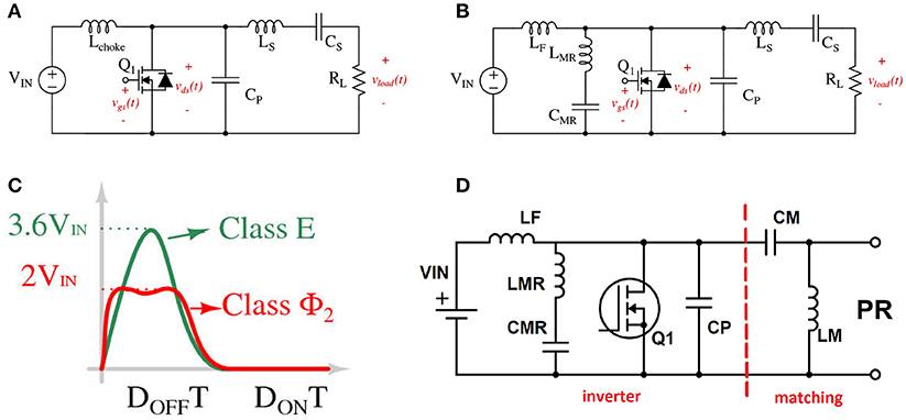
Figure 1. Class Φ2 inverter has 40% reduction on semiconductor voltage stress and all of the inductors are part of the resonant network and can be implemented without magnetic core. (A) Class E inverter, first investigated in 1964 by Gerald Ewing [19], has been widely used in telecommunication applications. (B) Class Φ2 inverter. (C) Drain Voltage Comparison. (D) Class Φ2 with a high pass L matching network to drive an electro-thermal plasma micro-thruster (Pocket Rocket PR type [20]) for CubeSat propulsion.
Particularly for this work, a class Φ2 switched mode dc-RF power inverter topology [17] as shown in Figure 1B is chosen. The class Φ2 inverter uses a novel multi-resonant network (LF, LMR, CMR, and CP in Figure 1B) to achieve zero voltage switching (ZVS) characteristics for the single ground reference semiconductor switch. ZVS is an important attribute for switched mode dc-RF power inverters as it eliminates the frequency dependent semiconductor switching losses and therefore allows efficient operations at switching frequencies up to 100 MHz [18]. The multi-resonant network also shapes the semiconductor switch off-state voltage waveform to approximate a trapezoidal with the maximum voltage stress to be about 2 times of the input voltage, a significant reduction compared to the 3.6 times of a class E inverter, as illustrated in Figure 1C. This allows designers to use better semiconductor devices with lower voltage ratings, which usually feature lower on-state resistance, better switching characteristics and therefore can lead to better converter efficiency. More importantly, the use of the multi-resonant network eliminates any large value choke inductors, e.g., required in a class E inverter, leaving all inductors part of the resonant network and of smaller inductance values. However, the Φ2 inverter, like many other switched mode topologies, is only capable of driving a relatively small range of loads efficiently compared to their linear mode counterparts. Unfortunately, plasma (a hot ionized conducting gas) as an electrical load is notoriously difficult to drive. The voltage-current (V-I) characteristics of plasma discharges are highly nonlinear, and extraordinarily sensitive to variations of parameters and operating conditions such as gas pressure, gas flow, driving voltage and power, etc. At each operating condition, small parameter changes can result in significant electrical impedance variations, leaving it difficult to maintain efficient soft switching power converter operation. Hence, it requires careful characterization of the plasma electrical impedance as well as design of matching networks to ensure efficient operation for plasma generation as illustrated in Figure 1D. These procedures are detailed in the section 5.
The next key feature is to use air core toroidal inductors to replace magnetic cored inductors, and to directly print them on the printed circuit board (PCB) using copper traces and vias. As switching frequency increases, magnetic components (inductors, transformers, etc), which often dominate the size and weight of power supplies, can have smaller values and sizes. Particularly, at beyond 10 MHz, any heavy and brittle ferromagnetic inductor cores which induces core losses that increase faster with switching frequency can be eliminated and replaced by air core inductors [21]. At this frequency range, not only inductance values become small enough to be compatible with air core designs, but air core inductors may also bring several advantages to the system. Specifically, performance (e.g., quality factor Q) of air core magnetic components improves as switching frequency increases (). Also, air core inductors are not limited by current saturation or by a Curie temperature limit, therefore offering much better linearity over wide operation range compared to their cored counterparts. Moreover, modern fabrication techniques [e.g., PCB [22–29], 3D printing [30], etc.] can be leveraged to reduce weight and cost without sacrificing performance.
Specifically, the PCB air core inductors presented here are toroidal in shape. Compared to more common air core spiral and solenoid shape inductors [23, 24, 31–34], toroids have the advantage of confining majority of the magnetic flux within the torus. This leads to reduced electromagnetic interference (EMI) with other components especially in a compact system. To predict inductance values of air core toroidal inductors, we use the following equation in Sullivan et al. [35], where N is turn number, and do, di, h denote outer, inner diameter and height of the toroid, respectively.
The first part of the equation represents the inductance from the flux within the torus structure while the second part calculates the “one turn” inductance induced by the circumferential direction current when it travels through the toroid as illustrated in Figure 2A. Toroidal inductors tend to have good quality factors when they have close to square shape cross sections [35]. Hence normal PCBs with a standard thickness of 1.6 mm limit maximum inductance value from the torus structure if maintaining a square cross section. We have been using thick PCBs (3.2 mm [29] and 6.4 mm [36]) instead to achieve a good balance between good electrical performance and simple fabrication process. Moreover, we also designed automated scripts to generate the copper traces shapes, vias locations, and layout files for PCB inductors, which further simplies the design process as mentioned in Liang et al. [28]. For different current carrying capabilities and operating frequencies, copper weight/thickness (e.g., 2 oz or more) can also be specified in the PCB fabrication process. Printing air core inductors on PCB takes the advantages of low part to part variation, streamlined manufacturing, and low prototyping cost of the PCB process and can benefit significantly for high frequency (beyond 10 MHz) power converters.
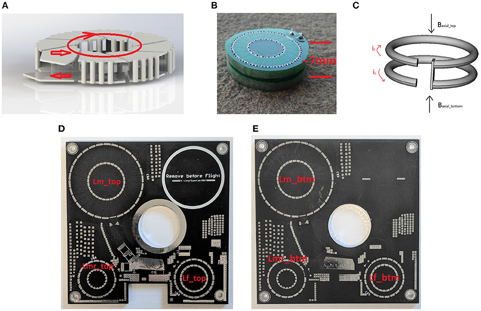
Figure 2. Class Φ2 inverter and matching network PCB design with all air core inductors printed on PCB. The stacking of the top and bottom board allows cancellation of axial flux form each toroidal inductor and mitigates EMI issue. (A) Schematics of the PCB toroidal air core inductor. The top and bottom of the toroid are copper planes on PCB and the vertical connections are made through vias. Note that as the current enters and exits at the toroid's two terminals, it creates a circumferential current path as indicated in the figure. The circumferential current induces axial flux outside the torus. (B) By vertically stacking two PCB toroidal inductors with the same dimensions and turns but opposite winding directions, the axial flux of the two toroids cancels and therefore mitigates EMI issue. The top and bottom toroids can be connected either in series or in parallel. (C) A simple schematic illustrates the axial flux cancelation effect. (D) Top half of the power inverter printed on a 3.2 mm thickness PCB. Note that not only a single inductor can be implemented with the stacking approach but also the whole inverter. This allows the axial flux cancelation of all the toroidal inductors in the inverter. (E) Bottom half of the power inverter printed on a 3.2 mm thickness PCB. Note that not only a single inductor can be implemented with the stacking approach but also the whole inverter. This allows the axial flux cancelation of all the toroidal inductors in the inverter.
To further mitigate the external flux caused by the “one turn” inductance that contributes to EMI, each air core inductor is also split into two double (or half) values connected in parallel (or series) with the same dimensions but opposite circumferential current directions. The two double (or half) valued inductors are then printed on two vertically stacked boards, as shown in Figures 2B,C, to cancel axial direction flux induced outside the torus [37]. Notice that the reduction of flux in the radial direction between the two inductors is less effective than in the axial direction. However, the most significant component of external flux in a toroidal inductor is due to the “one turn” inductance, that is, the field produced by the net current flowing along the circumference of the toroidal structure. The flux component in the radial direction resulting from stray fields leaking from between conductor turns only accounts for a small portion of the total external flux. Moreover, a toroid is a preferred means to implement an inductor that tries to minimizes total external flux, compared to other widely used structure to implement inductors like spirals and solenoids. It is possible to reduce external fields even further, by implementing EMI shields using additional layers of PCB. Addressing potential issues with EMI through layout and shielding are areas we will incorporate in future designs and prototypes.
By applying this technique, the class Φ2 inverter and the required matching network are implemented on two stacked 3.2 mm thickness PCBs. Figures 2D,E show the unpopulated top half and bottom half PCBs for the circuit. All the inductors in the circuit are already fabricated onto the PCBs leaving empty pads for placing capacitors and MOSFET. The PCB material used in this initial prototype is normal FR4. Advanced materials such as ceramic based or metal core substrate will be further explored to improve the PCB thermal and mechanical properties as the testing environment gets closer to more realistic spaceflight conditions.
2.2. Micro Electro-Thermal Plasma Thruster TinyPR
The Tiny Pocket Rocket (TinyPR) is developed at the Australian National University (ANU) as one of the Pocket Rocket Series electro-thermal plasma micro-thrusters for CubeSats [20]. Figures 3A,B show the assembly view and schematics of the TinyPR. For miniaturization purpose, only the core components such as the RF electrode, the plenum (gas inlet cavity), and the insulating macor part which defines both the 24 mm outer diameter housing and the 1.5 mm-diameter and 18 mm-long cylindrical plasma cavity, are kept. The reduction in size allows the integrated thruster and the power inverter PCB to serve as one side panel of CubeSat, occupying minimal footprint in precious CubeSat on board volume. More propellant and/or payload can be added from the saved volume. The Ar (or Xe, N2, CO2) gas propellant is fed though the 15 mm-diameter plenum (pressure of a few torr) creating a chocked flow into the smaller diameter plasma cavity. RF power is supplied at the electrode, creating an asymmetric weakly ionized (less than 1%) capacitively coupled plasma (CCP) inside the tube [38]. Plasma heating of the propellant will increase its exhaust velocity and therefore provide extra thrust than just passing through cold gas [39]. Physics details in the process have been well studied, modeled and detailed in the literature [20, 39–43] and the direct thrust measurement on a thrust balance has also been reported [43].
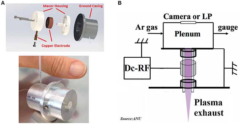
Figure 3. The micro electro-thermal plasma thruster TinyPR developed at ANU. (A) Assembly view of the TinyPR, the smallest Pocket Rocket series electro-thermal micro thruster developed at ANU. (B) Schematics of the TinyPR [20].
3. Power Inverter and Micro-Thruster Integration
Figure 4 shows the populated power inverter with the TinyPR mounted on the PCB. Note that as a proof of concept prototype, practical issues such as board fabrication and material use, MOSFET gate drive circuit, all RF connectors, etc are not optimized for spaceflight conditions. Component values (corresponding to Figure 1D) are as following, MOSFET part No.=IPD530N15N3, LF=63 nH, LMR=85 nH, LM=833 nH, CMR=390 pF, CP=390 pF, CM=120 pF. Latest development includes integration with the compact gas propellant system developed at ANU [44] and testing undertaken at ANU's WOMBAT facility, a 2 meter-long 1 meter-diameter vacuum chamber. Figures 5A,B shows the integrated design working in a 3D printed 1U CubeSat frame. The TinyPR is fed with 40 sccm of Ar gas flow and produces a plasma plume at its exhaust. The integrated thruster and power converter weighs about 150 g and has a footprint of about 10 cm by 10 cm by 7 mm while the TinyPR protrudes about 15 mm. Also note that there is no parasitic discharge shown on the board at a chamber pressure of about 0.3 μtorr. The power converter, operating at switching frequency of 13.85 MHz, draws about 45 W peak power at 14 V dc input and can be bursted at much lower rate to achieve below 1 W average power consumption to accommodate low power budget on board CubeSats. Under these conditions, the efficiency of the power converter is estimated as 85%. The output voltage and current waveforms are captured and analyzed in Figure 6.
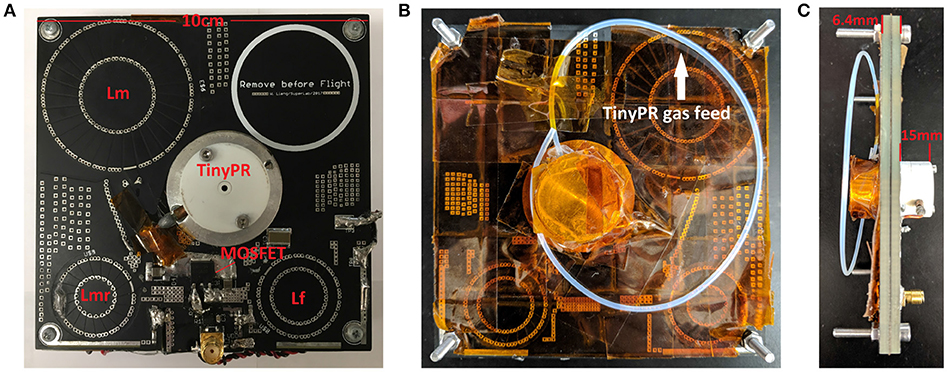
Figure 4. Integration of the power delivery system and the micro-thruster. Note that as a proof of concept prototype, practical issues such as board fabrication and material use, MOSFET gate drive circuit, all RF connectors, etc are not optimized for spaceflight conditions. (A) The TinyPR, outer diameter of about 24 mm, is mounted on the PCB inverter that powers it. This working assembly is designed to serve as a single CubeSat side panel. It occupies minimal footprint as a CubeSat plasma micro thruster. (B) The back side of the integrated TinyPR and power inverter. A plastic tube can be connected to the gas subsystem as gas feed for the TinyPR. (C) The side-view of the integrated TinyPR and power inverter.
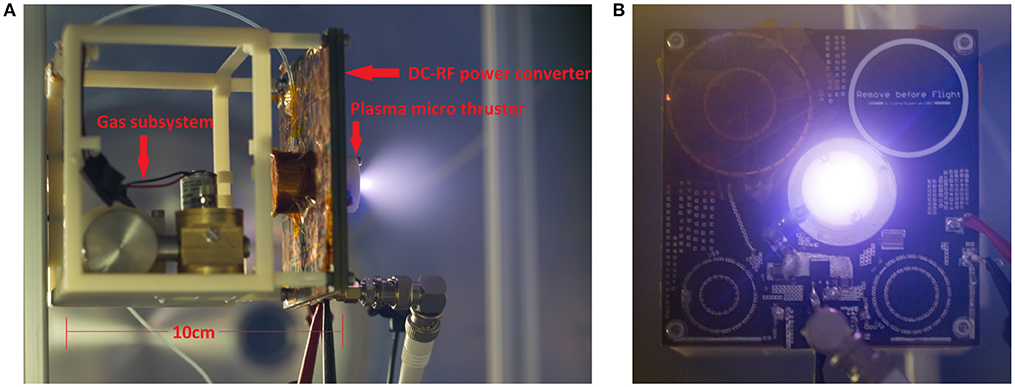
Figure 5. Operational testing of the integrated micro-thruster/power inverter 1 U CubeSat assembly in the ANU WOMBAT space simulation facility (A) side-view also showing gas subsystem integrated prototype [44]. (B) front-view demonstrating successful vacuum testing (no parasitic discharge) under space conditions.
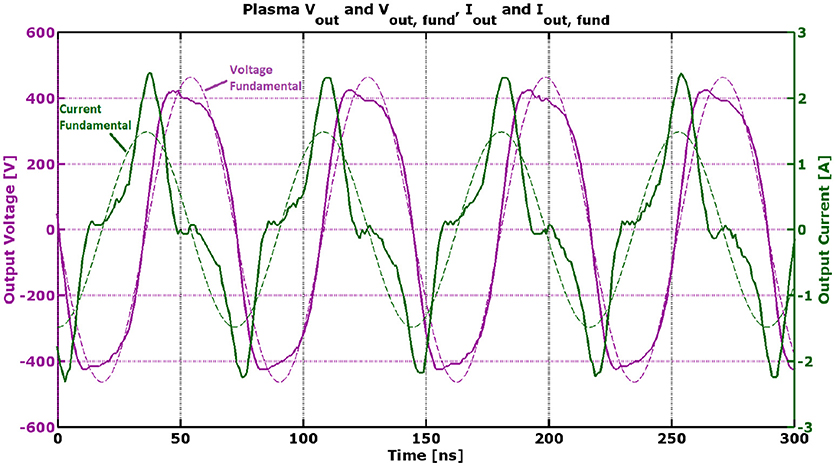
Figure 6. Measured voltage (purple solid) and current (green solid) waveforms of the TinyPR with plasma running. Assuming majority of the power is transferred at fundamental frequency, the extracted fundamental components of the voltage (purple dash) and current (green dash) are used to calculate impedance magnitude and phase.
In future iterations, peripheral systems such as battery unit and wireless gate drive control unit can be incorporated easily to increase the technology readiness level (TRL) as they have already been demonstrated in the Stanford University vacuum chamber. With the system occupying well under 1U, the advantages over other commercial available or in-development micro thruster systems are significant. It provides flexibility of reconfiguration for overall CubeSat design and mission planning, such as adding more gas propellant for longer thruster operation, or reducing overall CubeSat volume when combining payload into the thruster 1U allocation. It is also possible to have multiple integrated thruster and power converter systems on different CubeSat sides for more complex maneuvering at different axis.
4. Conclusion
Here we present a compact and efficient switched mode dc-RF power inverter integrated with an electro-thermal plasma micro-thruster intended to use on board CubeSats. Moreover, the power inverter uses only air core inductors which can be printed using copper traces and vias on Printed Circuit Board (PCB), resulting a planar and mechanical strong structure suitable for integration with the micro-thruster. In this way, the integrated power delivery and micro-thruster system can be used as side panels and structural support of CubeSats, saving precious on board volume for propellant and/or payloads.
5. Methods
5.1. Characterization of Plasma Impedance
To determine electrical impedance of plasma, we started by driving the micro-thruster to strike and maintain the plasma at intended operating conditions using an ENI A1000 linear RF power amplifier, as it is designed to drive a wide range of load. An RF coaxial current monitor (Pearson Model 6027) and a Rigol 100X voltage probe were inserted in line to measure the time domain current and voltage waveforms at the micro-thruster's input.
One important aspect to notice is that, as the proposed electro-thermal micro-thruster, TinyPR, is inherently capacitive with its impedance phase close to -90 degree, it is critical to prevent phase measurement error at tens of MHz range due to the probes themselves and/or difference in probe cables lengths, which can lead to drastically different impedance results. Hence a 50 Ω RF resistor with low parasitics as a standard was used as load to carefully calibrate and de-skew the voltage and current probes before measurements.
We supplied the RF power at 13.85 MHz from the ENI A1000 to TinyPR's electrode while feeding 40 sccm of Ar flow, both at its designed operating conditions. And we were able to measure voltage and current waveforms while maintaining the plasma in TinyPR. And Figure 6 shows the corresponding current and voltage waveforms of the TinyPR while plasma is running at designed power level of about 38 W with an estimated power inverter dc to plasma efficiency of 85 % [36] (Pplasma,OUT = PDC × 0.85 = 45 × 0.85 W = 38 W). Assuming majority of the power is transferred at fundamental frequency, the fundamental components of the voltage and current are also extracted (from analyzing the measurement waveform data) to determine the impedance magnitude and phase as shown as dash lines in Figure 6. The plasma impedance is then determined as ZMEAS = 37 − 284j Ω.
5.2. Lumped Element Matching Network Design
The switched mode dc-RF power inverter such as the Class Φ2 presented in this paper requires resistive or slightly inductive load to maintain zero voltage switching (ZVS) for efficient operation. But as indicated above, the measured impedance is highly capacitive. To transform the impedance to a resistive value, an L shape matching network as shown in Figure 7A is utilized. The matching network performs two functions, resonant to absorb the imaginary part of the load impedance, and transform the real part of the load to a value that the power inverter stage can work efficiently at designed power level. The derivation is as following,
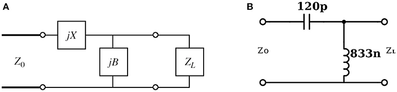
Figure 7. L shape matching network design. (A) one of the L shape matching network. (B) The designed matching network used in TinyPR converter.
To design the inverter to deliver Pplasma,OUT = 38 W at an input VIN = 14 V, according to the equation in Rivas et al. [17], about 4.2 Ω is needed at the inverter load.
So to achieve the transformation from ZL = 37 − 284j Ω to Zo = 4.2 Ω at 13.85 MHz, the following values are calculated for a high pass L shape matching network as shown in Figure 7B. The primary reason to choosing a high pass design is to allow CM to replace the large blocking CS in the original class Φ2 inverter as shown in Figure 1.
Author Contributions
The thruster power supply concept was discussed by all authors. The converter prototype was designed and manufactured by WL, LR, and JR-D at Stanford University. The gas subsystem and vacuum facility were prepared by AS, CC, and RB at the Australian National University. The prototype converter testing was done by WL, CC, and AS at the Australian National University. All authors contribute to data analysis and manuscript preparation.
Conflict of Interest Statement
The authors declare that the research was conducted in the absence of any commercial or financial relationships that could be construed as a potential conflict of interest.
The handling editor and reviewer SM declared their involvement as co-editors in the Research Topic, and confirm the absence of any other collaboration.
References
1. NASA. Benefits Stemming from Space Exploration. NASA. (2013) Available online at: https://www.nasa.gov/sites/default/files/files/Benefits-Stemming-from-Space-Exploration-2013-TAGGED.pdf
2. Li X, Selesnick R, Schiller Q, Zhang K, Zhao H, Baker DN, et al. Measurement of electrons from albedo neutron decay and neutron density in near-Earth space. Nature (2017) 552:382–5. doi: 10.1038/nature24642
3. Asphaug E, Thangavelautham J, Klesh A, Chandra A, Nallapu R, Raura L, et al. A cubesat centrifuge for long duration milligravity research. npj Microgravity. (2017) 3:16. doi: 10.1038/s41526-017-0021-0
4. Hand E. CubeSat networks hasten shift to commercial weather data. Science (2017) 357:118–9. doi: 10.1126/science.357.6347.118
5. Fink M, Rodriguez-Aramendia A, Handsteiner J, Ziarkash A, Steinlechner F, Scheidl T, et al. Experimental test of photonic entanglement in accelerated reference frames. Nat Communic. (2017) 8:7. doi: 10.1038/ncomms15304
6. Battersby S. Inner Workings: CubeSats set to tackle living systems, effects of deep space radiation. Proc Natl Acad Sci USA. (2017) 114:10805–7. doi: 10.1073/pnas.1712815114
7. Chien S, Wagstaff KL. Robotic space exploration agents. Sci Robot. (2017) 2:eaan4831. doi: 10.1126/scirobotics.aan4831
8. Sokol J. Minisatellite surge spurs downlink infrastructure. Science (2017) 357:1342–3. doi: 10.1126/science.357.6358.1342
9. Tang Z, Chandrasekara R, Tan YC, Cheng C, Durak K, Ling A. The photon pair source that survived a rocket explosion. Sci Reports (2016) 6:25603. doi: 10.1038/srep25603
10. Tang Z, Chandrasekara R, Sean YY, Cheng C, Wildfeuer C, Ling A. Near-space flight of a correlated photon system. Sci Reports (2014)4:6366. doi: 10.1038/srep06366
11. Bahcivan H, Cutler JW, Springmann JC, Doe R, Nicolls MJ. Magnetic aspect sensitivity of high-latitude E region irregularities measured by the RAX-2 CubeSat. J Geophys Res. (2014) 119:1233–49. doi: 10.1002/2013JA019547
12. NASA. Cubesats Released From Space Station. NASA (2013). Available online at: http://www.nasa.gov/content/cubesats-released-from-space-station-0
13. Oltrogge D, Leveque K. An evaluation of cubesat orbital decay. In: Proceedings of the 25th Annual Aiaa/usu Conference on Small Satellites. Logan, UT (2011).
14. Qiao L, Rizos C, Dempster AG. Analysis and comparison of cubesat lifetime. In: Proceedings of the 12th Australian Space Development Conference. Adelaide, SA (2013).
15. Kim JY, Seo ES, Kim H, Park JW, Lim DK, Moon DW. Atmospheric pressure mass spectrometric imaging of live hippocampal tissue slices with subcellular spatial resolution. Nat Communic. (2017)8:2113. doi: 10.1038/s41467-017-02216-6
16. Privat-Maldonado A, O'Connell D, Welch E, Vann R, van der Woude MW. Spatial Dependence of DNA Damage in Bacteria due to Low-Temperature Plasma Application as Assessed at the Single Cell Level. Sci Reports (2016)6:35646. doi: 10.1038/srep35646
17. Rivas JM, Han Y, Leitermann O, Sagneri AD, Perreault DJ. A High-Frequency Resonant Inverter Topology With Low-Voltage Stress. IEEE Trans Power Electron. (2008) 23:1759–71. doi: 10.1109/TPEL.2008.924616
18. Pilawa-Podgurski RCN, Sagneri AD, Rivas JM, Anderson DI, Perreault DJ. Very-High-Frequency resonant boost converters. IEEE Trans Power Electron. (2009) 24:1654–65. doi: 10.1109/TPEL.2009.2016098
20. Charles C, Boswell RW. Measurement and modelling of a radiofrequency micro-thruster. Plasma Sourc Sci Technol. (2012)21:022002. doi: 10.1088/0963-0252/21/2/022002
21. Glaser JS, Nasadoski J, Heinrich R. A 900W, 300V to 50V Dc-dc power converter with a 30MHz switching frequency. In: APEC 2009 Twenty-Fourth Annual IEEE Applied Power Electronics Conference and Exposition, 2009. Washington, DC (2009). p. 1121–8.
22. Zolog M, Pitica D, Pop O. Characterization of Spiral Planar Inductors Built on Printed Circuit Boards. In: 30th International Spring Seminar on Electronics Technology. Cluj-Napoca (2007). p. 308–13.
23. Andersen TM, Zingerli CM, Krismer F, Kolar JW, O'Mathuna C. Inductor optimization procedure for Power Supply in Package and Power Supply on Chip. In: Energy Conversion Congress and Exposition (ECCE), 2011. Phoenix, AZ: IEEE (2011). p. 1320–7.
24. Vanek J, Szendiuch I, Hladik J. Optimization of properties of planar spiral inductors. In: 30th International Spring Seminar on Electronics Technology. Cluj-Napoca (2007). p. 235–8.
25. Orlandi S, Allongue BA, Blanchot G, Buso S, Faccio F, Fuentes CA, et al. Optimization of sheilded PCB air-core toroids for high efficiency dc-dc converters. IEEE Trans Power Electron. (2011) 26:1837–46. doi: 10.1109/TPEL.2010.2090902
26. Kamali-Sarvestani R, Williams JD. Fabrication of high quality factor RF-resonator using embedded inductor and via capacitor. In: IECON 2010 - 36th Annual Conference on IEEE Industrial Electronics Society. Glendale, AZ (2010). p. 2283–7.
27. Tang SC, Hui SY, Chung HSH. Coreless printed circuit board (PCB) transformers with multiple secondary windings for complementary gate drive circuits. IEEE Trans Power Electron. (1999) 14:431–7.
28. Liang W, Glaser J, Rivas J. 13.56 MHz high density DC-DC converter with PCB inductors. IEEE Trans Power Electron. (2015)30:4291–301.
29. Raymond L, Liang W, Choi J, Rivas J. 27.12 MHz large voltage gain resonant converter with low voltage stress. In: Energy Conversion Congress and Exposition (ECCE), 2013. Denver, CO: IEEE (2013). p. 1814–21.
30. Liang W, Raymond L, Rivas J. 3-D-Printed Air-Core Inductors for High-Frequency Power Converters. IEEE Trans Power Electron. (2016) 31:52–64. doi: 10.1109/TPEL.2015.2441005
31. Nour Y, Ouyang Z, Knott A, Jrgensen IHH. Design and implementation of high frequency buck converter using multi-layer PCB inductor. In: IECON 2016 - 42nd Annual Conference of the IEEE Industrial Electronics Society. Florence (2016). p. 1313–7.
32. Tang SC, Hui SY, Chung HSH. Coreless planar printed-circuit-board (PCB) transformers-a fundamental concept for signal and energy transfer. IEEE Trans Power Electron. (2000) 15:931–41. doi: 10.1109/63.867683
33. Raju S, Wu R, Chan M, Yue CP. Modeling of mutual coupling between planar inductors in wireless power applications. IEEE Trans Power Electron. (2014) 29:481–90.
34. Rivas JM. Radio Frequency dc-dc Power Conversion. Ph.D. thesis, Massachusetts Institute of Technology, Cambridge, MA (2006).
35. Sullivan CR, Li W, Prabhakaran S, Lu S. Design and fabrication of low-loss toroidal air-core inductors. In: Proceedings of IEEE Power Electronics Specialists Conference PESC 2007. Orlando, FL (2007). p. 1754–9.
36. Liang W, Raymond L, Davila JR, Charles C, Boswell R. Structurally supportive RF power inverter for a CubeSat electrothermal plasma micro-thruster with PCB inductors. In: 2017 IEEE Applied Power Electronics Conference and Exposition (APEC). Tampa, FL (2017). p. 2141–5.
37. Liang W, Raymond L, Gu L, Rivas J. 27.12MHz GaN resonant power converter with PCB embedded resonant air core inductors and capacitors. In: 2015 IEEE Energy Conversion Congress and Exposition (ECCE). Montreal, QC (2015). p. 4251–6.
38. Greig AD. Pocket Rocket: An Electrothermal Plasma Micro-thruster. Ph.D. thesis, The Australian National University, Canberra, ACT (2015).
39. Ho TS, Charles C, Boswell R. Neutral gas heating and ion transport in a constricted plasma flow. Phys Plasmas. (2017)24:084501. doi: 10.1063/1.4996014
40. Boswell R, Charles C, Alexander P, Dedrick J, Takahashi K. Plasma expansion from a radio frequency microdischarge. IEEE Trans Plasma Sci. (2011) 39:2512–3. doi: 10.1109/TPS.2011.2143434
41. Greig A, Charles C, Boswell RW. Simulation of main plasma parameters of a cylindrical asymmetric capacitively coupled plasma micro-thruster using computational fluid dynamics. Front Phys. (2015) 2:80. doi: 10.3389/fphy.2014.00080
42. Charles C, Bish A, Boswell RW, Dedrick J, Greig A, Hawkins R, et al. A short review of experimental and computational diagnostics for radiofrequency plasma micro-thrusters. Plasma Chem Plasma Process. (2016) 36:29–44. doi: 10.1007/s11090-015-9654-5
Keywords: plasma thruster, electric propulsion (EP), power electronics, Cubesat, Space Exploration
Citation: Liang W, Charles C, Raymond L, Stuchbery A, Surakitbovorn K, Gu L, Boswell R and Rivas-Davila J (2018) An Integrated RF Power Delivery and Plasma Micro-Thruster System for Nano-Satellites. Front. Phys. 6:115. doi: 10.3389/fphy.2018.00115
Received: 12 July 2018; Accepted: 18 September 2018;
Published: 12 October 2018.
Edited by:
Gianpiero Colonna, Consiglio Nazionale Delle Ricerche (CNR), ItalyReviewed by:
Andrea Cristofolini, Università degli Studi di Bologna, ItalySergey Macheret, Purdue University, United States
Copyright © 2018 Liang, Charles, Raymond, Stuchbery, Surakitbovorn, Gu, Boswell and Rivas-Davila. This is an open-access article distributed under the terms of the Creative Commons Attribution License (CC BY). The use, distribution or reproduction in other forums is permitted, provided the original author(s) and the copyright owner(s) are credited and that the original publication in this journal is cited, in accordance with accepted academic practice. No use, distribution or reproduction is permitted which does not comply with these terms.
*Correspondence: Wei Liang, bGlhbmd3QGFsdW1uaS5zdGFuZm9yZC5lZHU=