 Mostafa Agour
 Fabian Thiemicke1
 André F. Müller
 Claas Falldorf
- 1BIAS-Bremer Institut für angewandte Strahltechnik, Bremen, Germany
- 2Physics Department, Faculty of Science, Aswan University, Aswan, Egypt
- 3MAPEX Center for Materials and Processes and Faculty of Physics and Electrical Engineering, University of Bremen, Bremen, Germany
We explore the principles, implementation details, and performance characteristics of a lensless multi-spectral digital holographic sensor and demonstrate its potential for quality assurance in semiconductor manufacturing. The method is based on capturing multi-spectral digital holograms, which are subsequently utilized to evaluate the shape of a reflective test object. It allows for a compact setup satisfying high demands regarding robustness against mechanical vibrations and thus overcomes limitations associated with conventional optical inspection setups associated with lens-based white light interferometry. Additionally, the tunable laser source enhances the versatility of the system and enables adaptation to various sample characteristics. Experimental results based on a wafer test specimen demonstrate the effectiveness of the method. The axial resolution of the sensor is
1 Introduction
In the fast-evolving landscape of the chip industry, the pursuit of quality is paramount to ensure the reliability and functionality of semiconductor devices (Bechtler and Velidandla, 2003; Krauter et al., 2017). Quality inspection, particularly at the wafer level, is a critical task that demands axial precision in the nanometer range across an extent of several tenths of microns (Colonna de Lega and De Groot, 2005; Strapacova et al., 2017).
Established methods for optical inspection (Osten, 2018), such as white light interferometry (WLI) and confocal microscopy, have been instrumental in achieving high resolution (De Groot and Deck, 1995; Vogel et al., 2011). However, their application in in-production or in-line quality inspection has been hindered by severe challenges (Agour et al., 2015). Traditional optical inspection methods face practical limitations due to their sensitivity to mechanical disturbances during the acquisition process (Bergmann et al., 2021). In addition, they are subject to other distortions from various sources, including optical system imperfections (such as misalignment and focusing errors), dust and reflections (Migukin et al., 2013). Moreover, the sophisticated imaging systems associated with these methods are not only expensive but also heavy, rendering them inflexible and slow.
This paper introduces an innovative approach aimed at overcoming these challenges by using a lensless digital holographic sensor paired with a wavelength-tunable laser as the light source. This approach is based on our recently developed fullfield lensless acquisition of spectral holograms or Flash-WLI (Falldorf et al., 2023). Unlike traditional systems, this configuration captures multi-spectral digital holograms, which are subsequently utilized to evaluate the shape of a reflective specimen under test. The lensless digital holographic sensor brings a paradigm shift in wafer-level inspection, overcoming the limitations towards robustness and flexibility of conventional white-light interferometers. Its compact design eliminates the need for complex imaging systems, providing flexibility and ease of integration into existing production lines. Furthermore, the sensor’s ability to operate in a mechanically less constrained environment enhances its suitability for in-line applications. The wavelength tunability of the laser source adds an extra degree of freedom to the versatility of the system, allowing adaptability to different specimen characteristics.
In this publication, we delve into the principles, implementation, and performance of the lensless digital holographic sensor in the context of in-line wafer-level inspection. We present experimental results based on a wafer test specimen, showcasing its efficacy in providing precise, nanoscale-resolution measurements. The proposed method not only addresses the shortcomings of current inspection techniques but also paves the way for enhanced efficiency, cost-effectiveness, and adaptability in the dynamic realm of chip manufacturing.
2 Methods
Figure 1 shows the basic setup of Flash-WLI (Falldorf et al., 2023). It represents a Michelson type interferometer with the reflective specimen in one of the interferometer arms. Let us denote the recorded intensity in the sensor domain by (Schnars et al., 2015):
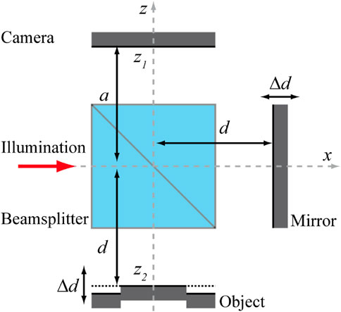
Figure 1. The concept of Flash-WLI: The setup is a simple Michelson type interferometer that enables the recording of digital holograms of the object under test. The camera sits at a distance
In Equation 1
from a single recorded hologram (Takeda et al., 1982). The basic idea is to record multiple digital holograms with different wavelengths
which can be used to numerically calculate the result of a measurement with short coherent illumination, where the coherence length depends on the bandwidth. The coherence function, given by Equation 3, will be maximum for light reflected by parts of the object that share the same optical path to the camera like the reference wave reflected by the mirror. However, in order to determine those object parts, we have to propagate the entire coherence function into the object plane
with
where
again, we can add the spectral modes to yield the coherence function in the object plane
Hence, similar to white light interferometry, the shape of the object can be retrieved by progressively changing the length of
which can be seen from replacing
In Equation 9, the height map
Finally, to ensure a good sampling of the spectral density and optimally select the wavelengths, one needs to set
where N denotes the number of discrete lines required to perform the measurement. This means the unambiguity range, given by Equation 10, equals N times the depth of focus
3 Results and discussions
The experimental setup used to demonstrate the proposed method is shown in Figure 2A. This configuration is derived from the schematic shown in Figure 1. In order to achieve the modulation of the interference pattern with the spatial carrier frequency necessary for the extraction of individual coherence functions from the corresponding digital holograms, the reference mirror of the interferometer is tilted accordingly. The test object, represented by the wafer test microstructures shown in Figure 2B, is positioned at a distance of
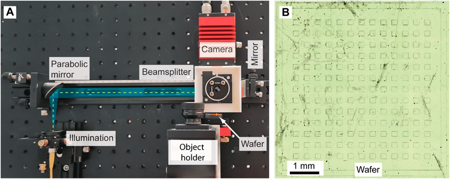
Figure 2. Experimental Flash-WLI setup employing spectral holography: (A) Photograph depicting the beam path of the Flash-WLI setup. Initially, a parabolic mirror collimates a spherical wave, which is subsequently split into object and reference waves through a
A wavelength-tunable dye laser having a range starting from 560 nm to 615 nm served as a manually tuned light source in conjunction with a HeNe laser emitting at 632.8 nm and a solid-state laser at 488 nm, respectively, to expand the spectral width of the illumination. In the context of digital holography, the numerical aperture remains approximately constant for each object point, given by
The field of view is limited by the object side numerical aperture (the angle that the object includes with any pixel of the camera). Thus, the FOV could be simply increased by increasing the distance between the camera and the object. If the resolution shall be preserved, the number of pixels must be increased, because in this case the space-bandwidth-product of the imaging process is increased (the image provides more information).
To capture a set of data, the dye laser was manually tuned from 572 nm to 604 nm in 1 nm increments, resulting in the acquisition of 33 multi-spectral digital holograms of the wafer under test. Additionally, two holograms were captured with the supplementary laser sources at 488 nm, and 632.8 nm. To calibrate the measurement system, we also captured digital holograms with a flat reference mirror placed in the object plane. The multi-spectral digital holograms of the object measurements were thus calibrated by subtracting the phase distributions of these reference measurements for every individual wavelength.
Please note that the camera exposure time is less is about 1 ms but the AVT used can only capture 20 frames per second. However, the tunable laser is manually adjusted so that each capture takes approximately 5 s. As a result, it takes about 3 min to capture all the holograms required. This time-consuming process could be improved by using a faster camera and automating the laser tuning.
However, an important result of this study is that the number of frames required for a measurement is at least one order of magnitude smaller when compared to white-light interferometers, which are often used for similar tasks.
Figures 3A, B examplarily show the amplitude and phase distributions of the complex amplitude reconstructed from the hologram captured at
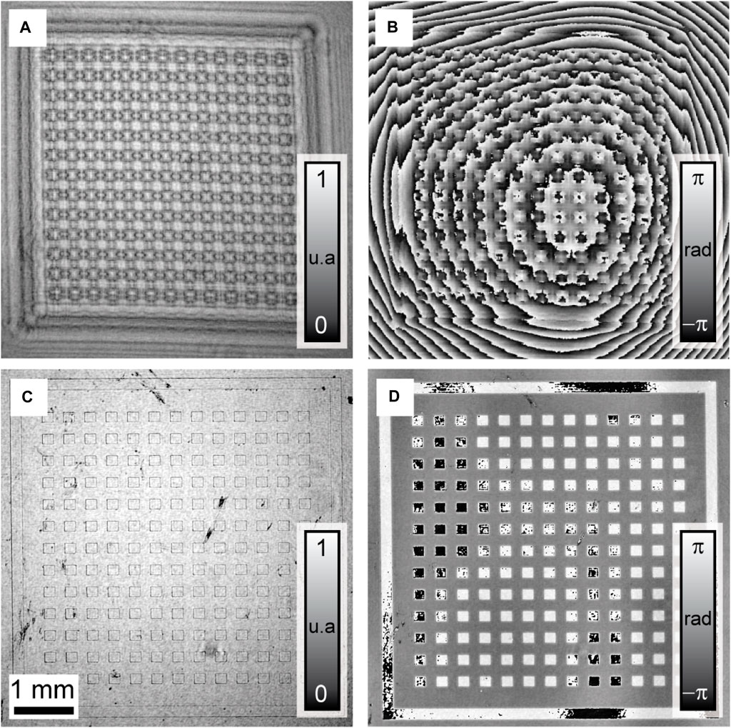
Figure 3. (A,B) show the amplitude and phase of a single spectral mode
Now, applying the methodology outlined in Section 2 we calculate the coherence function along the
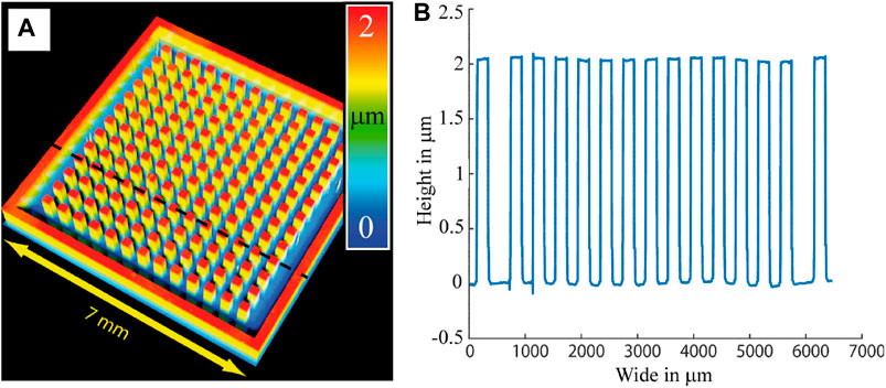
Figure 4. The obtained 3D profile: (A) A height map of the wafer microstructure, and (B) the profile across the dashed black line in (A). The map shows square microstructures with an average height of
An analysis of the local surface fluctuations across flat areas of the wafer reveals a deviation of
4 Conclusion
In this work, we have investigated the principles, implementation details and performance of the lensless multi-spectral digital holographic sensor, i.e., Flash-WLI, and demonstrated its potential in the field of semiconductor manufacturing. The method is based on the acquisition of digital holograms captured at different wavelengths. These holograms are then used to evaluate the shape of a reflective test object. Unlike WLI, Flash WLI is a lensless, robust and compact design that overcomes the limitations associated with conventional optical inspection methods such as lens-based WLI, including high requirements for mechanical vibration and bulky and heavy imaging configurations.
The experimental results, derived from the examination of a wafer sample, serve to demonstrate the effectiveness of the sensor in providing high accuracy measurements. The reported measurement uncertainty of
The successful application of the sensor in semiconductor manufacturing is a significant step forward, paving the way for improved microstructure analysis and quality control in wafer manufacturing.
Data availability statement
The raw data supporting the conclusions of this article will be made available by the authors, without undue reservation.
Author contributions
MA: Conceptualization, Data curation, Investigation, Methodology, Validation, Visualization, Writing–original draft, Writing–review and editing. FT: Data curation, Investigation, Methodology, Validation, Writing–original draft. AM: Data curation, Investigation, Visualization, Writing–original draft. RB: Funding acquisition, Supervision, Writing–review and editing. CF: Conceptualization, Formal Analysis, Investigation, Methodology, Supervision, Validation, Writing–original draft, Writing–review and editing.
Funding
The author(s) declare that financial support was received for the research, authorship, and/or publication of this article. The authors are grateful to the State of Bremen for funding of this work through the program “Forschung, Entwicklung und Innovation” (FEI) within the frame of the project “Linsenlose Mikroskopie für die industrielle Qualitätskontrolle” (LiM-Q), project no. FUE0665B and to the Deutsche Forschungsgemeinsdchaft (DFG) for funding parts of the work in the context of the project “Shape measurement by means of imaging using partially coherent illumination” (Spice II), project no. 284158589.
Acknowledgments
The authors are grateful to Reiner Klattenhoff for technical support with the setup and the image acquisition system.
Conflict of interest
The authors declare that the research was conducted in the absence of any commercial or financial relationships that could be construed as a potential conflict of interest.
Publisher’s note
All claims expressed in this article are solely those of the authors and do not necessarily represent those of their affiliated organizations, or those of the publisher, the editors and the reviewers. Any product that may be evaluated in this article, or claim that may be made by its manufacturer, is not guaranteed or endorsed by the publisher.
References
Agour, M., Riemer, O., Flosky, C., Meier, A., Bergmann, R. B., and Falldorf, C. (2015). Quantitative phase contrast imaging of microinjection molded parts using computational shear interferometry. IEEE Trans. Ind. Inf. 12, 1623–1630. doi:10.1109/tii.2015.2481704
Bechtler, L., and Velidandla, V. (2003). Optical surface analysis: a new technique for the inspection and metrology of optoelectronic films and wafers. Integr. Opt. Devices Fabr. Test. 4944, 109–116. doi:10.1117/12.468295
Bergmann, R. B., Kalms, M., and Falldorf, C. (2021). Optical in-process measurement: concepts for precise, fast and robust optical metrology for complex measurement situations. Appl. Sci. 11, 10533. doi:10.3390/app112210533
Colonna de Lega, X., and De Groot, P. (2005). “Optical topography measurement of patterned wafers,” in AIP conference proceedings (American Institute of Physics), 788, 432–436.
De Groot, P., and Deck, L. (1995). Surface profiling by analysis of white-light interferograms in the spatial frequency domain. J. Mod. Opt. 42, 389–401. doi:10.1080/09500349514550341
Falldorf, C., Thiemicke, F., Müller, A. F., Agour, M., and Bergmann, R. B. (2023). Flash-profilometry: fullfield lensless acquisition of spectral holograms for coherence scanning profilometry. Opt. Express 31, 27494–27507. doi:10.1364/oe.493711
Goodman, J. W. (2005). Introduction to fourier optics. Englewood, CO: Roberts and Company publishers.
Krauter, J., Gronle, M., and Osten, W. (2017). Optical inspection of hidden mems structures. Opt. Meas. Syst. Ind. Insp. X 10329, 272–280. doi:10.1117/12.2269499
Migukin, A., Agour, M., and Katkovnik, V. (2013). Phase retrieval in 4f optical system: background compensation and sparse regularization of object with binary amplitude. Appl. Opt. 52, A269–A280. doi:10.1364/ao.52.00a269
Schnars, U., Falldorf, C., Watson, J., and Jüptner, W. (2015). Digital holography and wavefront sensing. 2 edn. Berlin Heidelberg: Springer-Verlag.
Strapacova, T., Priewald, R., Jerman, T., and Mentin, C. (2017). “Inline wafer edge inspection system for yield enhancement of thin wafers,” in 2017 28th annual SEMI advanced semiconductor manufacturing conference (ASMC) (IEEE), 138–143.
Takeda, M., Ina, H., and Kobayashi, S. (1982). Fourier-transform method of fringe-pattern analysis for computer-based topography and interferometry. JosA 72, 156–160. doi:10.1364/josa.72.000156
Keywords: white light interferometry, digital holography, optical inspection, shape measurement, wafer inspection
Citation: Agour M, Thiemicke F, Müller AF, Bergmann RB and Falldorf C (2024) Lensless multi-spectral holographic interferometry for optical inspection. Front. Photonics 5:1416347. doi: 10.3389/fphot.2024.1416347
Received: 12 April 2024; Accepted: 15 July 2024;
Published: 05 August 2024.
Edited by:
Maciej Trusiak, Warsaw University of Technology, PolandReviewed by:
Michał Józwik, Warsaw University of Technology, PolandAdam Styk, Warsaw University of Technology, Poland
Copyright © 2024 Agour, Thiemicke, Müller, Bergmann and Falldorf. This is an open-access article distributed under the terms of the Creative Commons Attribution License (CC BY). The use, distribution or reproduction in other forums is permitted, provided the original author(s) and the copyright owner(s) are credited and that the original publication in this journal is cited, in accordance with accepted academic practice. No use, distribution or reproduction is permitted which does not comply with these terms.
*Correspondence: Mostafa Agour, YWdvdXJAYmlhcy5kZQ==