 Carl Hägglund
- Division of Solar Cell Technology, Department of Materials Science and Engineering, Uppsala University, Uppsala, Sweden
With the success of silicon (Si) solar cell technology, research and development on higher efficiency multijunction solar cells is gaining much attention. Tandem cells with a perovskite top cell and a Si bottom cell show particular potential. However, the optical modeling of such devices is complicated by the broad range of length scales involved; the optically thin layers and nanoscale features of a perovskite solar cell require some version of wave optics or even full field electromagnetic (EM) calculations, while the micrometer scale structuring and large dimensions of Si cells are much more manageable using geometrical (ray) optics. In the present work, a method for combining EM and ray optical calculations is developed and described in detail, with examples provided in the software Comsol Multiphysics. For regions with thin films or nanoscale features, EM wave calculations are performed using the finite element method. These calculations provide the phase and amplitude of the waves diffracted into different orders, of which only the regular reflection and transmission are typically of relevance for nanoscale periodicity. In the ray optics simulation, the corresponding regions are implemented as diffracting interfaces, with deterministic transformations of the Stokes vector components according to the EM wave calculations. Meanwhile, the absorbed intensity of intersecting rays is recorded. The method is applied to separate perovskite and Si solar cells and to a few tandem solar cells of relevance for two- versus four-terminal configurations. Corrections for strongly absorbing media in the ray tracing algorithm, which use generalized versions of the Fresnel coefficients, Snell’s law and the Beer-Lambert law, are also evaluated. In a typical Si solar cell with a front surface structure of inverted pyramids, such corrections are found to reduce the absorption by up to 0.5 percentage units compared to a conventional ray tracing calculation. The difference is concluded to originate mainly from reduced absorption rates of inhomogeneous waves, rather than from enhanced escape probabilities for (quasi-) trapped rays at the Si front surface. The method is further applied to evaluate the effects of a plasmonic nanoparticle array, embedded in a perovskite solar cell stack that is located directly on the microstructured Si surface.
1 Introduction
The wave-particle duality of light can be connected to small and large length scales, where the full physics of electromagnetic (EM) waves must be considered on length scales near or below the wavelength, while the behavior of light is well described by particle-like rays on the large scale. Full field EM calculations account for the electromagnetic field components, including their phases, coherent interaction, and deviations from propagating wave solutions in the near-field region around scattering objects, such that precise solutions to Maxwell’s equations are obtained. Rays, on the other hand, are localized representations of pure propagating wave solutions to Maxwell’s equations. At a given instant in time, each ray can be associated with a position, propagation direction, intensity and polarization, and via ray tracing techniques, the ray trajectory and interaction with its environment can be calculated. To fully represent ray polarization, including randomly polarized (unpolarized) states, the four component Stokes vector can be used. Thereby, the ray approximation can be very useful in applications involving large structures, where full EM wave calculations are impractical due to the computational demands.
Perovskite-silicon tandem solar cells involve both large and small scale structures, where light trapping can play a significant role for the performance (Schneider et al., 2014; Jošt et al., 2018; Jäger et al., 2020). Because of the weak absorption in Si and the consequently thick (∼100 µm) Si layers used in a Si bottom cell, full EM wave calculations become computationally expensive for the whole optical domain and are usually replaced or complemented by other methods. Indeed, ray tracing has long been the method of choice for optical modeling of Si solar cells (Yablonovitch, 1982; Brendel, 1995; Rodríguez et al., 1997). Meanwhile, the thin (∼1–∼100 nm) layers of the perovskite solar cell (PSC), contact stacks and any parts of the device with dimensions on the order of the wavelength or below, require a more refined EM wave treatment for accurate results. A multiscale approach for bridging EM wave optics and ray optics in different parts of the tandem device is thus attractive.
Varying approaches to the multiscale problem in solar cells have been implemented, (Rothemund et al., 2013; Tucher et al., 2015; Lokar et al., 2018; Tucher et al., 2018; Santbergen et al., 2017) often using some combination of the transfer matrix method (Byrnes, 2016) for one dimensional (1D) modeling of EM wave optics, with 2D or 3D ray optics for the larger scale (Lipovšek et al., 2011; Holst et al., 2013). This situation is schematically illustrated in Figure 1A. If periodic surface structures are considered, as illustrated in Figure 1B, diffraction into discrete forward and backward directions result. These can produce a computationally manageable number of diffraction orders if the pattern period is sufficiently small, (Mellor et al., 2011; Rothemund et al., 2013) permitting the ray optics calculation to be performed in a deterministic manner. Rather than assigning the outcome of interactions stochastically, the ray intensity is then divided and distributed over the diffraction orders according to calculated diffraction amplitudes. In the simplest, small grating limit, these amplitudes agree with the reflectance and transmittance of the structure, where the reflected ray direction is obtained from the law of reflection, and the refracted direction from Snell’s law. Finally, scattering into a continuum of directions by arbitrary, non-periodic small scale structures may also be considered, as illustrated in Figure 1C. In this case, the surface scattered rays are usually assigned through an approximate analytical model for the bidirectional scattering distribution function, (Jäger et al., 2012) of which the uniform Lambertian distribution is a common choice. More specific analytical functions or interpolated data from model calculations can alternatively be used, although the latter may entail full EM wave calculations for a much larger geometrical domain and a squared number of angles compared to the case of a discrete diffraction grating. A probabilistic approach such as the Monte Carlo method, or binning into discrete directions, (Tucher et al., 2015) is then typically used to limit the number of scattered rays for the ray tracing calculation.
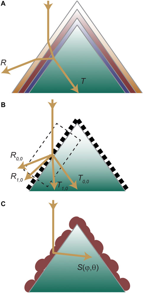
FIGURE 1. (A) Specular reflection (R) and refraction/transmission (T) in directions given by the law of reflection and Snell’s law, through one or several thin films. (B) Diffraction by a small scale grating, with the lowest order components (0,0) in the same directions as for (A). (C) General scattering by rough surface, into a continuum of directions
In the present work, a method is presented for combining periodic small scale features modeled by EM wave calculations, with an overall geometry modeled by ray tracing. In the small scale part, illustrated by the dashed box in Figure 1B, periodicity is assumed in the surface plane and the finite element method (FEM) with Floquet boundary conditions is used for 3D modeling, as implemented in the electromagnetic wave module of the software from Comsol Multiphysics. The resulting grating structure gives rise to discrete diffraction orders. For simplicity, structures where only the lowest order diffraction is allowed are considered in this work, but the model may readily be generalized to account for larger periods by the inclusion of higher diffraction orders. Randomly organized small-scale structures may also be accommodated as long as an effective medium approximation is valid. Thus periodic nanostructures and any number of thin layers can be accommodated as an interface layer on larger (>10 µm) periodic or non-periodic structures, as further illustrated in Figure 2.
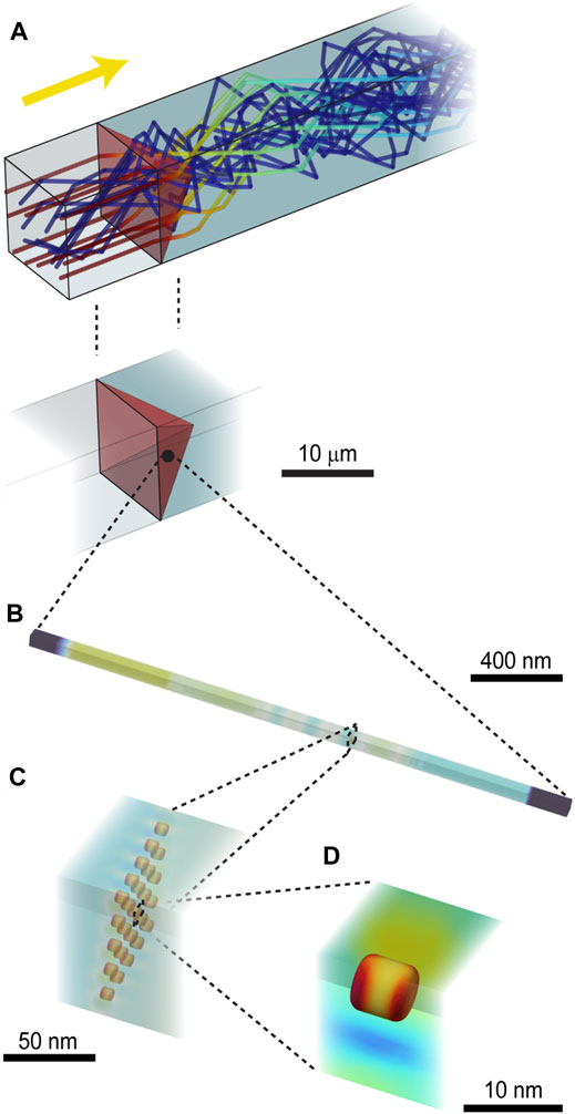
FIGURE 2. (A) Part of a geometry used for ray tracing in a perovskite-Si tandem solar cell of relevance for 2-terminal devices. Rays are launched at the left interface in the normal direction, as shown by the yellow arrow. The multilayered stack of the perovskite top cell is in this particular configuration located directly on the oblique inverted pyramid surfaces at the front of the Si bottom cell, highlighted by the red surfaces in the cutout. When rays intersect this interface, their reflected and transmitted Stokes vector components are assigned according to EM wave calculations for the perovskite stack, such as the one shown in (B). The perovskite stack may also include nanoscale patterns, here in form of a gold nanoparticle array as shown in (C), with its unit cell in (D).
Applied to the case of a simple, planar stack, this approach will provide the precise optical response by releasing and tracing a single ray and its secondary rays until extinction. When the optical path length depends on the initial ray position, as for a microstructured solar cell, statistics obtained for a large number of rays is on the other hand usually desired. For instance in Figure 2A, the periodic inverted pyramid structure at the Si front surface produces different ray traces depending on the points of intersection, and a relatively large number of rays must be traced to determine the average absorption in the Si solar cell.
The use of the model is illustrated by its application to perovskite-Si tandem cell geometries of relevance for two-terminal (2T) and four-terminal (4T) configurations, as well as to a tandem cell with a nanopatterned layer in the form of a gold nanoparticle array, see further Figure 3. While there are many specialized software available for ray tracing applications, Comsol Multiphysics can be used to combine a very broad range of physics, for instance including thermal and semiconductor physics of relevance for solar cells (Gauthier and Hägglund, 2020). It deploys a powerful approach to geometrical optics based on Stokes vector formalism and non-sequential wavefront tracing, (Mizuyama, 2017) with a convenient implementation of corrections for absorbing media. The latter are of some relevance since refraction and reflection at oblique angles between lossy media produce inhomogeneous waves with the planes of constant amplitude deviating in orientation from the planes of constant phase (Dupertuis et al., 1994a; Dupertuis et al., 1994b; Chang et al., 2005). As a further application of the presented method, this often neglected aspect for the absorption in regular Si solar cells is briefly evaluated and discussed. The main goal of the present work is to provide an accessible method for the optical modeling of tandem solar cells on the length scales of importance, with a detailed description of the method implementation accompanied by executable simulation files.

FIGURE 3. Basic configurations considered, including (A) a planar 4T version of a PSC-Si tandem, (B) a microstructured 4T version of a PSC-Si tandem, (C) a microstructured 2T version of a PSC-Si tandem and (D) a microstructured 2T version of a PSC-Si tandem where the PSC is nanopatterned.
2 Materials and Methods
The typical tandem cell configurations considered in this work are illustrated in Figure 3. The optical constants of all materials used in the calculations are described below and also provided as tabulated data files in the Supplementary Material. Examples of executable Comsol Multiphysics model files are also provided in the Supplementary Material.
2.1 Perovskite Solar Cell Definition
The layers of the perovskite solar cell are summarized in Table 1. The front glass is modeled based on the Pilkington TEC15 glass, of 1.8 mm thickness. This soda lime glass has a conductive F:SnO2 (FTO) layer with a sheet resistance of 15 Ω/□. The thicknesses and optical constants of the transparent conductive stack were provided by Chen (2010). The layers were found to consist of 28.7 nm SnO2, 22.2 nm SiO2 and 353.3 nm FTO, with an estimated surface roughness of 27.3 nm. The interfacial roughness resulting from this is in the present work taken into account using the two-component Bruggeman effective medium approximation (EMA), with the optical constants of the surrounding layers as inputs (Niklasson and Granqvist, 1984). The filling and depolarization factors are assumed fixed at 0.5 and 1/3, respectively. To determine the physically correct root from the Bruggeman equation, the Wiener bounds are used as described by Jansson and Arwin (1994). Thus the EMA-1 layer in Table 1 models a mixture of FTO and nickel oxide. Similarly, EMA-2 models a mixture of perovskite and C60, and EMA-3 that of IZO and EVA. Additional materials in the PSC stack included 10 nm nickel oxide (NiO) with optical constants from Ghosh, (Ghosh et al., 2015) 15 nm C60 using data from Horiba Scientific, (Horiba Scientific, 2015) and 210 nm indium-zinc-oxide (IZO) as the back contact, here roughly approximated by a Cody-Lorentz oscillator (Ferlauto et al., 2002) fitted to a spectroscopic ellipsometry measurement of In2O3 (see further the tabulated data file provided in the Supplementary Material).
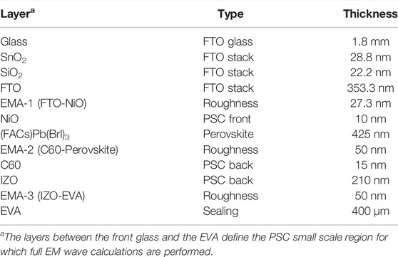
TABLE 1. PSC stack, from front to back, including surrounding media.
For the perovskite absorber layer, the optical properties of a mixed halide metal perovskite [(FACs)Pb(BrI)3] were modeled using three Kramers–Kronig consistent Forouhi-Bloomer oscillators, (Horiba Scientific, 2006; Löper et al., 2015) adapted to roughly match the bandgap (1.55 eV) and measured quantum efficiency of a (non-optimized) bare top cell prepared by the solar cell company Evolar AB. In this adaption, the thicknesses of some of the layers in the stack were slightly adjusted to improve the fit to experimental data, see further Table 1.
In the case Au nanoparticles were included in the PSC model, the optical constants for Au were taken from Weaver and Frederikse (Weaver et al., 2002) and used without accounting for surface scattering or other corrections for the nanoscale dimensions.
2.2 Si Solar Cell Definition
The PERC type Si solar cell is common in production, (Green et al., 2021) and is therefore chosen as a starting point for the bottom cell here (see Table 2). In the calculations, a Si absorber layer of 180 µm thickness is assumed unless otherwise stated. The Si optical constants are taken from Herzinger, (Herzinger et al., 1998) although some results were also reproduced using the tabulated refractive index and absorption coefficient from Green, at 300 K (Green, 2008). The Si front surface is assumed to be structured with a regular array of inverted pyramids of base 10 µm and depth 7.07 µm, giving the characteristic 54.7° etch angle between the top (100) surface plane and pyramid (111) sides. For simplicity, metal contact fingers and flat surfaces in-between or at the base of the pyramids are neglected in the calculations. Silicon nitride (SiNx) with a thickness of 80 nm is assumed as a passivating and antireflective coating (ARC) on top of the Si structure (Fell et al., 2015). The SiNx optical constants were obtained by fitting a Kramers–Kronig consistent Cody-Lorentz oscillator function to data from Duttagupta, (Duttagupta et al., 2012) considering the case for a NH3/SiH4 ratio equal to 3 (c.f. data file in the Supplementary Material). The front of the Si cell is assumed to be sealed with a 400 µm thickness layer of EVA polymer, using the optical properties reported by Vogt for conventional EVA (Vogt et al., 2016). Finally, the back contact is modeled as a planar 200 nm SiO2 layer on Al, (Fell et al., 2015) with optical constants from (Herzinger et al., 1998) and (Smith et al., 1997), respectively.
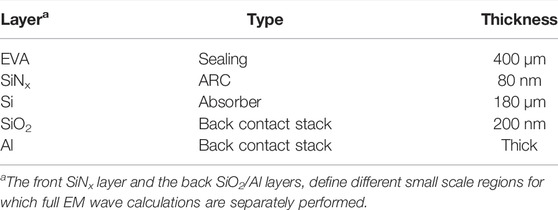
TABLE 2. Si solar cell layers, from front to back.
2.3 Electromagnetic Wave Calculations
For stacks of thin layers and nanostructured materials, the EM fields must be calculated with phase for an accurate description. This is done in separate 3D models for each of the small scale regions defined in Table 1, 2, prior to the ray optics calculations. For stacks of only uniform, homogeneous layers, 1D calculations by for instance the transfer matrix method are fully sufficient. However, when layers are rough or deliberately structured, modeling in 2D or 3D can be required. A full 3D EM wave model is therefore developed and implemented by the finite element method, using the electromagnetic waves, frequency domain module of Comsol Multiphysics. An example Comsol model file is included as Supplementary Material.
In these calculations, light is considered incident on a stack of layers with a structure of lateral periodicity
Full EM wave calculations were separately performed for the small scale regions corresponding to the PSC, the SiNx ARC, and the SiO2/Al back contact stack (Table 1, 2), to determine the absorptance of each individual layer, and the reflectance and transmittance into the surrounding media. The phases of reflected and transmitted waves were also obtained. To cover all pure (s- and p-) polarized states, calculations were performed for both incident transversal electric (TE) and transversal magnetic (TM) waves, for wavelengths from 300 to 1,200 nm in steps of 10 nm, and for angles of incidence (
Using a PC with 16 GB RAM and an Intel Core i7-7700 processor at 3.6 GHz and depending on the requirements for the meshing, the solution time varied between 3 and 9 s per wavelength and angle of incidence. This summed up to a total solution time between 14 and 40 h when considering all combinations of the conditions specified above.
2.3.1 Boundary Conditions
Periodicity was simulated at the varying angles of incidence by invoking Floquet boundary conditions for all domain boundaries orthogonal to the planes of the stack. Cartesian perfectly matched layers (PMLs) were used to simulate semi-infinite extent of the surrounding entrance and exit media, with scattering boundaries as the external terminations (Comsol Multiphysics, 2021a). To account for the dependence of projected wavelength components on
2.3.2 Meshing
The bulk of the geometry was meshed using tetrahedral elements with a maximum size adapted to the minimum wavelength in the different parts of the stack, for instance below 6 nm in the high refractive index Si part of the structure. The PMLs used elements swept from the boundary elements of the tetrahedral mesh along the stack normal, and was divided into 30 slices distributed according to an exponential distribution where the spacing was close (∼1 nm) next to the bulk of the model and more sparse further away. For calculations with Au nanoparticles, a mesh size down to 0.03 nm was deployed in the high field regions defined by the nanoparticle surface curvature and the incident electric field, such that energy was conserved to within ∼0.1% in the simulations.
2.3.3 Ports and Paddings
Homogeneous plane waves of defined polarization, angle of incidence
1 Volume integration of the absorption may suffer in accuracy next to a source boundary, where fields are discontinuous.
2 At high
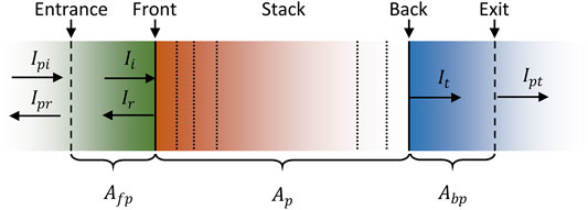
FIGURE 4. Arrangement of entrance and exit ports around the layer stack for EM wave calculations. The absorptance of the front and back paddings (
To address these issues, padding layers are introduced between the entrance/exit ports and the front/back interfaces of the stack. The paddings are chosen small enough (here 20 nm) to transmit substantial intensity at all wavelengths, see further Figure 4.
To derive the reflectance and transmittance when the entrance and exit media are absorbing, the absorption in the front and back padding layers (
Considering the absorption loss in the back padding, the transmittance becomes,
Similarly, absorptance in the stack and analogously in its individual layers, is obtained from,
To determine
Substituting
where only the positive sign is valid in lossy media where
By definition,
For the phase difference between TM and TE waves (retardance
2.4 Ray Optics Implementation
The ray optics module of Comsol Multiphysics version 6.0 is used to build a model for the complete tandem cell here, as described in detail in the Supplementary Material and further illustrated by the provided Comsol model file. Position, wavevector, intensity, phase, wavefront curvature and polarization is traced for each released ray and its secondary rays in the geometry. The polarization, as defined by the Stokes vector, defines the electric field intensity within a local coordinate system attached to each ray, with the x-axis along the direction of propagation, and the y- and z-axes defined by the wavefront curvature (Comsol Multiphysics, 2021b). The 4-component Stokes vector describes the total ray intensity in
The transversal axes of the ray coordinate system are arbitrarily oriented in relation to the plane of incidence (PI) of surfaces in the geometry, where the latter is spanned by the direction of ray propagation and the surface normal. Before determining the interaction of a ray with a grating interface, the Stokes vector is therefore rotated an angle
The surface stack reflection is now imposed through a Mueller matrix multiplication, (Comsol Multiphysics, 2021b),
where
Similarly, the partially normalized, transmitted (refracted) Stokes vector is obtained from,
where
Finally, absorptance in the stack as a whole or in individual layers is obtained from,
where
2.4.1 Ray Optics Simulations
In the ray optics simulations, the trajectories of rays are calculated as a function of time. Several rays, typically in bundles of 10, are released from quasi-random positions at normal angle of incidence from the front surface of the geometry. These rays are fully polarized, and all rays within the same bundle have the same linear polarization vector, which is varied randomly for each bundle. For microstructured cells, it is here necessary to trace around 200 rays to estimate the average behavior.
During calculations, progress is followed by a number of probes, where the overall ray intensity/power and accumulated sum of absorption, reflection and/or transmission out of the geometry are the most important. This enables energy conservation to be checked continuously. At the end, the accumulated absorption in different parts, as well as the reflectance and transmittance (if any), are exported for statistical analysis.
On the regular PC used for this work, the average solution time was about 2 s/ray, although it was much higher for the longest wavelengths (see further below). This translates to a total solution time of 10 h for 200 rays evaluated at steps of 10 nm in wavelength.
2.4.2 Accuracy and Ray Economy
For long wavelengths, the absorption coefficients in Si and other parts of the geometry are very low, and some rays will propagate a long distance before extinguishing. As the rays split for every reflection/refraction event, their number grows exponentially with time and can easily produce an unmanageable situation. To avoid this and still obtain accurate data, it is therefore useful to implement a threshold intensity, below which rays are cut off as they will no longer contribute significantly to the overall energy balance. In the current model an intensity threshold is set to
The number of secondary rays (produced by reflection/scattering) are pre-allocated, and a higher number requires more computational resources. It is important to allocate a sufficient number of secondary rays, so that reflections of intense rays are never suppressed in favor of weaker ones towards the end of the simulation. For long wavelengths, especially beyond the bandgap threshold at about 1,120 nm for Si, the requirement for secondary rays increases more or less exponentially with wavelength as the optical path length increases. Statistics for the number of used secondary rays from initial simulations is useful for pre-allocation at each wavelength.
For related reasons it is also important to minimize the distance traveled through non-essential parts of the geometry, as long passage times lead to exponential growth of secondary rays from the many reflection and refraction events of other rays in smaller domains. Assuming a perfectly anti-reflective front surface, internal reflections are suppressed there and the Beer-Lambert law can account for the absorption in the front layer (glass or EVA here). Only a thin layer (10 µm) is then included in the actual ray optics geometry. A very small overestimation of the reflectance arises from the fraction of light that is reflected at the back of the front medium and would have been absorbed in the excluded thick layer of glass or EVA, but is rather counted towards the reflectance.
There are several other factors which together determine the accuracy of the simulation, in particular the maximum time step for the solver. As a reference, the speed of light is in the range of 43–86 μm/ps in Si (for 300–1,200 nm wavelength). With too large time steps, the solver fails to detect internal surfaces in the geometry. For short wavelengths, absorption takes place in about 0.001 ps. On the other hand, it can take several hundred ps to extinguish long wavelength light in Si. To accommodate these different time scales, the maximum time step is limited to 0.01 ps below 600 nm wavelength, 0.1 ps below 800 nm, 1 ps below 1,130 nm, and 5 ps from 1,130 to 1,200 nm.
The spatial resolution of the mesh can be relatively crude, even exceeding the wavelength (∼1 µm) in the bulk and down to ∼0.1 µm around sharp features/corners of the geometry.
A final important condition, is the overall stopping criterion used for the simulation. Here, the summed intensity of all active rays is used such that the simulation is stopped when less than a small fraction (10–3 when
2.5 Photocurrent Calculations
Photocurrent densities are (Jsc) calculated under the assumption of perfect internal quantum efficiency. The absorptance
Here,
3 Results
3.1 Ray Optics Evaluation
It is useful to monitor the energy balance of simulations, by comparing the incident intensity (
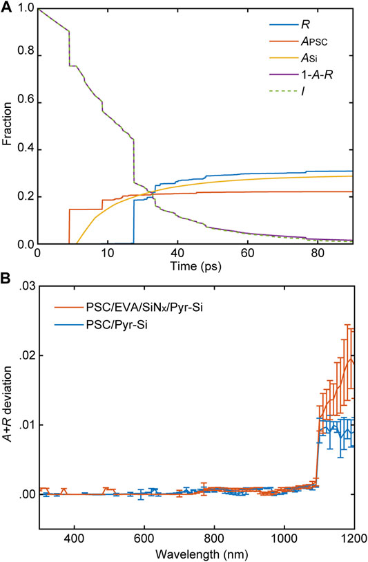
FIGURE 5. (A) Time evolution for reflection and absorption in the PSC and Si solar cell layers of a tandem cell, at 1,100 nm wavelength. The PSC absorption occurs mainly in the TCO layers and the initial 10% intensity loss is due to absorption in the glass. (B) Average
The difference
3.2 Application to Bare Si Solar Cells
As a reference case, the method is first applied to the bare Si solar cell described in Table 2, structured with inverted pyramids whose insides are coated by 80 nm SiNx serving as an ARC (Fell et al., 2015). The ARC can be modeled in a few different ways. If neglecting absorption in the film, thin film interference effects can be managed directly through the option to add a thin dielectric coating to material discontinuities in the Comsol ray optics module. As a second option, the treatment of SiNx as a dielectric coating is complemented with corrections for strongly absorbing media in the ray tracing algorithm, which have an effect due to the absorbing Si. With these corrections, basic relations such as Snell’s law and the Fresnel coefficients are modified and rays corresponding to inhomogeneous plane waves form upon refraction at oblique angles at the Si surfaces (Dupertuis et al., 1994a; Chang et al., 2005). Finally, the method of separate EM wave calculations presented in the present work, is applied to account for absorption in the SiNx thin film. Due to assuming periodicity in the EM wave calculations, inhomogeneous plane waves cannot generally be represented unless the lateral extent of the unit cell is large enough to accommodate a full beam profile. This is computationally expensive, especially at high angles of incidence, and in this work only homogeneous waves are considered in the EM wave calculations. Then, for consistency, corrections are not applied to ray tracing combined with EM wave calculations. The Si absorptance curves for the three different cases are shown in Figure 6A and summarized in Table 3, and their differences are highlighted in Figure 6B. These differences are small, but with interesting spectral dependences.
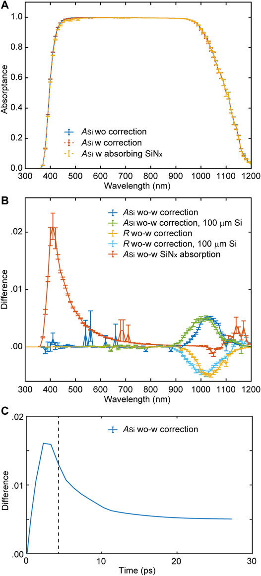
FIGURE 6. (A) Absorptance for a silicon solar cell with an 80 nm SiNx coating applied as an ARC. In the standard case, the SiNx is treated as a dielectric and no correction for absorbing media (Si) is performed. This is compared to the case with corrections but still a dielectric SiNx, and to the case without correction but full EM wave calculations for absorbing SiNx. (B) The differences in silicon absorption and reflectance without and with correction, for the regular (180 µm) and a thinner (100 µm) Si layer. The difference for a dielectric SiNx calculation and a full EM wave calculation for absorbing SiNx is also shown. (C) Average differences in silicon absorption without and with correction as a function of time, at 1,030 nm wavelength. The dashed line indicates the minimum time required for normal incident rays to be reflected at the Si back and return to the front interface.
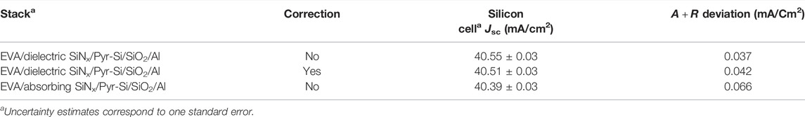
TABLE 3. Comparison of calculations for bare silicon solar cells.
The effect of the correction for absorbing media is studied with a dielectric SiNx, and it is found to reduce the Si absorptance by up to 0.5% in a region around 1,030 nm wavelength (Figure 6B). This is in the shoulder region where the Si absorptance declines due to the decreasing Si absorption coefficient with increasing wavelengths. As a consequence, a higher fraction of the intensity is absorbed in the backside metal layer or lost as it escapes at the front Si/SiNx interface after returning from backside reflection. It can be understood that the correction has a peak-like effect in this wavelength region, since for shorter wavelengths, all light entering the Si is absorbed both with and without correction. Meanwhile with longer wavelengths, as the Si absorption coefficient decreases, the correction becomes less important. This interpretation is supported by a calculation for a thinner, 100 µm thick Si absorber layer, where the maximum difference, shown in Figure 6B, shifts to a shorter wavelength by about 30 nm. Although the correction makes an overall difference in the integrated photocurrent of less than 0.1 mA/cm2 here, it is plausible that this would both grow and broaden spectrally with yet thinner absorber layers, since the absorption shoulder would then move further into a spectral region where the Si absorption coefficient is higher. It should be mentioned that a few outliers with more than 5% deviation from energy conservation were omitted in the analysis. These were associated with glitches where the ray intensity increased in an unphysical manner in the corrected runs. This turned out to be connected to a numerical instability associated with low ray intensity in the corrected runs, and could be amended by increasing the intensity cut-off threshold from
One may conceive of three contributions to the reduced Si absorption in the corrected calculations. First, the external reflection at the SiNx/Si front interface could in principle be enhanced by the correction, although this is not expected when the medium of incidence is non-absorbing. Second, rays corresponding to inhomogeneous waves with a non-zero inhomogeneity angle (
When comparing the calculation for dielectric SiNx with the full EM wave calculation performed with the more realistic absorbing SiNx coating, the difference (Figure 6B) again shows a maximum, but this time at wavelengths around 410 nm and with a peak amplitude of 2%. This can be understood as a consequence of the maximum in the product of the spectral dependence for the SiNx absorption coefficient—which increases with shorter wavelengths—and the transmittance of the EVA layer at the front of the cell—which increases with longer wavelengths. Weak oscillations may also be perceived in the long wavelength region. Overall, the effect of SiNx absorption is a reduction of the integrated short circuit current density by
Generally, the Si absorption spectra have a relatively slow sub-gap tail-off for the longest wavelengths, which may in part be due to the somewhat old data set used for the Si optical constants in these calculations (Herzinger et al., 1998). If instead using Si optical constants from Green, (Green, 2008), a more pronounced tail-off is indeed observed for wavelengths above 1,170 nm (not shown). The overall photocurrent also increases by about 0.1 mA/cm2, mainly due to higher absorptance in the shoulder region between 930 and 1,050 nm wavelengths.
It may finally be noted that with a less absorbing EVA layer, or with a bare Si cell, up to 1.4 mA/cm2 higher photocurrent could be gained, giving a total of 41.8 mA/cm2 when considering the realistic, absorbing SiNx ARC. This is comparable to the best Si solar cells reported to date, for instance at 41.6 mA/cm2 for the LONGi p-type PERC (Green et al., 2021). Slightly higher values could be realized with a microstructured back interface and a fully optimized ARC.
3.3 Tandem Solar Cells
When a PSC and Si solar cell are combined into a tandem cell, the photocurrent generation of the bottom cell changes strongly compared to its isolated response, but some modification also occurs for the top cell photocurrent because of the back reflection from the bottom cell. The changes depend on the detailed configuration. Here, both planar Si surfaces and microstructured Si front surfaces with inverted pyramids are considered, as they are commonly employed in Si solar cells (see Figure 3). The configurations include those where the top cell is separated from the bottom cell by a thick layer of polymer (here in the form of EVA, see Figures 3A,B), of relevance for a 4-terminal device, and those where the top cell is located directly on the Si top surface (see Figure 3C), of higher concern for a 2-terminal device. In the 4T case, it is here assumed that the PSC is always planar, while in the 2T case, the PSC layers are assumed to follow the local orientation of the Si surface. The considered geometries and their calculated photocurrents are summarized in Table 4. The corresponding calculated absorptance spectra are displayed in Figure 6.
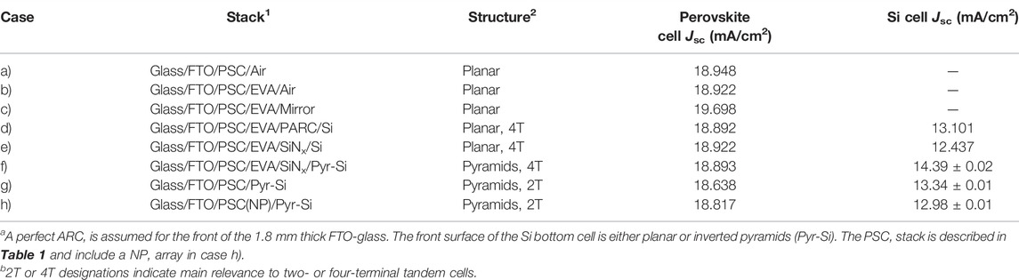
TABLE 4. Perovskite and perovskite/Si tandem cell evaluations.
For reference, calculations for a planar PSC with and without a 400 µm EVA polymer sealing on the back (Figure 7A and Table 4a and b), show a very small difference in the PSC photocurrent density of 0.02 mA/cm2. Thus the back reflection at the PSC/Air interface is only slightly higher than for the PSC/EVA and EVA/Air interfaces combined. It is also instructive to study the case where the back reflection at the EVA/Air interface is eliminated by a perfect ARC (PARC) on top of a Si bottom cell (Table 4d). This results in a PSC photocurrent density drop by another 0.03 mA/cm2. On the other hand, the effect of a perfect mirror backing the EVA is more significant (Table 4c), increasing the current density by 0.77 mA/cm2 compared to an EVA/air interface. The latter, basic light management, would bring the PSC photocurrent up to 19.7 mA/cm2 if it could be implemented as a long pass filter on the Si surface (Schneider et al., 2014). The effect is mainly observed on the shoulder of the PSC absorption curve, above 600 nm wavelengths (Figure 7A). This PSC photocurrent density is comparable to the 19.8 mA/cm2 reported for one of the highest efficiency perovskite-Si tandems so far, from HZB (Green et al., 2021).
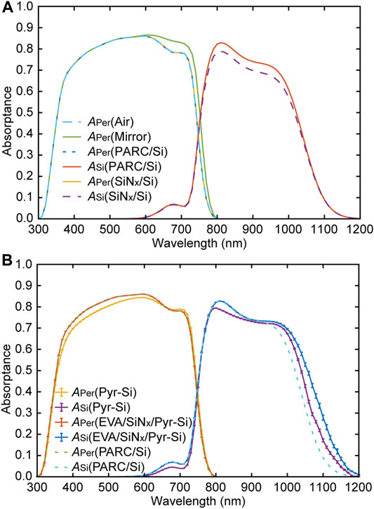
FIGURE 7. (A) Absorptance in the perovskite and Si layers for planar configurations including a bare PSC in air, a PSC with EVA backed by a mirror surface, a PSC with EVA and perfect ARC on Si, and a planar stack of PSC/EVA/SiNx/Si. (B) Absorptance for tandems with microstructured Si including PSC located directly on the Pyr-Si, or on a planarizing EVA layer (EVA/Pyr-Si). For reference, the curves obtained with a PARC on planar Si are also included. Error bars correspond to one standard error.
The effects of the intermediate layers are stronger on the photocurrent generation in the Si cell, as they filter (together with the rest of the PSC) all incident light. For example, the photocurrent density drops from 13.1 to 12.4 mA/cm2 when the PARC (Table 4d) is exchanged to the more realistic absorbing SiNx ARC (Table 4e) at the front of a planar Si solar cell.
For the 4T-case with an inverted pyramid Si front surface (Figure 3B), the planar PSC is separated from the Si by a 400 µm EVA intermediate layer. With an absorbing SiNx ARC, the Si cell produces a photocurrent density of 14.4 mA/cm2 (Table 4g), which is significantly higher than the 13.1 mA/cm2 for the case of a PARC on planar Si. The enhanced photocurrent generation in the long wavelength region results from the prolonged optical path length associated with the refraction and internal reflections of rays interacting with the obliquely oriented pyramid surfaces. Meanwhile, the reflection losses approach those with a PARC, as evident from the virtually identical spectra between 600 and 900 nm (Figure 7B).
This 4-terminal configuration may be compared to that of a PSC placed directly on top of the inverted pyramid Si surface, of higher relevance for a 2-terminal tandem cell (Figure 3C). Here, the SiNx is omitted in the calculation as it does not yield any benefit from an optical viewpoint. Without any other form of optimization however, the tandem cell performance is observed to decline in several respects. The PSC photocurrent density is reduced from 18.9 to 18.6 mA/cm2 due to increased reflection losses in a broad spectral range up to 650 nm wavelength, while it is only slightly enhanced near the PSC bandgap. Meanwhile the Si photocurrent density is reduced from 14.4 to 13.3 mA/cm2, despite reduced reflection losses overall. This is explained by a much enhanced parasitic absorption in the transparent conducting oxides of the PSC in the long wavelength region. Thus while this type of configuration can show benefits, it is clear that optimization of the tandem stack as a whole is required to avoid unnecessary losses. Further, the bandgap of the PSC may need to be increased in order to approach a higher current density in the Si part of this 2T configuration.
3.4 Nanostructured Tandem Cells
To demonstrate the capability of the method with regards to combinations of nanostructure and larger microstructures, calculations were finally performed for the geometry illustrated in Figure 2 and Figure 3D. Here, an array of gold nanoparticles (NPs) is located on top of the back interface of the perovskite absorber layer in the PSC. Such NPs may be of interest for enhancing the photocurrent generation via their localized surface plasmon resonance, as well as for improved contact conductivity in PSCs (Hägglund et al., 2016; Ai et al., 2022). The NPs were here assumed to be of cylindrical shape, of 5 nm height and 5 nm diameter, and with edges rounded with a radius of 1 nm. Although a chemical barrier coating would likely be required to preserve the metal NPs, this is neglected for simplicity. A spacing of 12 nm was chosen to preserve the unit cell size as in the rest of this work. EM wave calculations were performed for the corresponding PSC stacks located directly on the Si front surface, as for the 2-terminal configuration described above. The results, after ray optics calculations for the full tandem cell geometry were performed, are presented in Figure 8. A peak due to the plasmon resonance is found near the perovskite absorption edge, at 750 nm wavelength (Figure 8B). This is associated with a small positive effect on the perovskite absorption, corresponding to a photocurrent increase of 0.18 mA/cm2. On the other hand, as another 0.18 mA/cm2 is absorbed in the Au NPs themselves, the net effect in the Si layer is negative with a photocurrent reduction of 0.36 mA/cm2 compared to the case without NPs. The weak feature observed in the difference spectrum of the Si absorption slightly below 1,100 nm wavelength is likely an effect of the phase shift imposed by the NP array. Overall, the net photocurrent loss is close to the Au NP absorption of 0.18 mA/cm2 and a rebalancing of the photocurrents could readily be accomplished by means of a small adjustment of the perovskite layer thickness or bandgap. However, as the goal was mainly to demonstrate the method applicability here, such optimization was not performed.
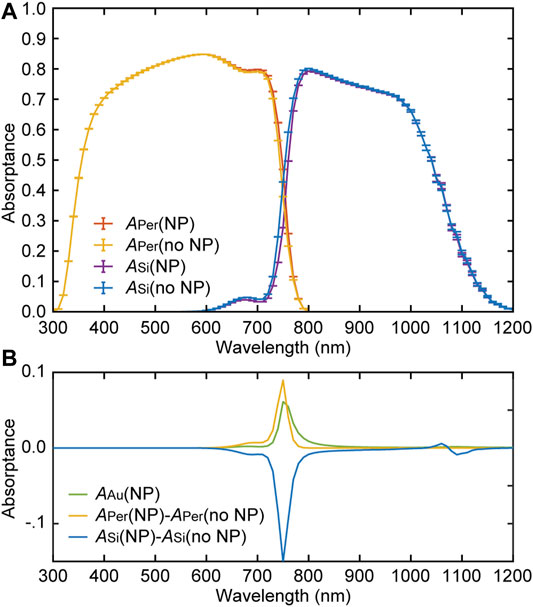
FIGURE 8. (A) Absorptance in the perovskite and Si layers with and without a gold NP array included at the back of the perovskite layer. (B) Absorptance in the Au NPs and the absorptance differences in the perovskite and Si layers with and without NPs.
4 Discussion
With the method demonstrated here for typical perovskite-Si tandem solar cells, more rigorous calculations with corrections for the ray tracing in absorbing media display slightly reduced Si photocurrents at longer wavelengths in comparison to standard calculations. Previous work estimated that such corrections become important in the context of ray optics when the extinction coefficient exceeds approximately 10% of the refractive index (Dupertuis et al., 1994b). Later analysis involving wedge shaped geometries on the other hand concluded that, for accurate treatment of polarized light, corrections are needed already for the corresponding ratio of 1% (Chang et al., 2005). These effects are nevertheless usually neglected or assumed negligible in ray optics calculations for solar cells, (Dahan et al., 2013; Lumb et al., 2014) and there appears to be no quantitative evaluation of the errors caused by this. It is thereby quite interesting that a reduction of 0.5 percentage units is observed here for the absorptance in a regular Si solar cell, for wavelengths between 1,000 and 1,100 nm where the extinction coefficient to refractive index ratio is less than 10–4. It is also quite interesting that the effect is found to originate from corrections to the effective absorption coefficient rather than from the more well-known correction to the total internal reflectance. A more extensive investigation would be needed to draw more general conclusions regarding its importance for ray tracing in solar cells, especially when applied to cells with thinner absorber layers and higher absorption coefficients. Nevertheless, the corrections observed in the present work have a small overall effect that is, for instance, less significant than the typical absorption losses in an 80 nm SiNx ARC.
In the current approach, regions with small scale layered and/or periodic structure are represented as grating interfaces in the ray optics calculations, with their properties (transfer functions) determined using EM wave calculations. In the EM wave calculations, light is assumed to be representable as homogeneous plane waves, such that periodic boundary conditions and a small unit cell can be used. Under these conditions, the treatment is rigorously correct. Importantly, this applies to sunlight incident at any angle on a periodic or stratified structure. Thus calculations for the first passage of sunlight through a thin, planar or nanostructured solar cell, will produce rigorously correct results with this method, at least as long as the transparent media in front of it can be considered non-absorbing from the viewpoint of wave homogeneity. As the corrections to the ray tracing are seen to have negligible effect in the spectral range of the top cell absorption, and this effect would only come into play via back reflected contributions, the non-corrected standard calculations will predict the top cell performance with excellent accuracy.
Should one consider Si absorber thicknesses on the order of 10 µm using a ray optics approach, the correction for strongly absorbing media could be more important and require an appropriate treatment of inhomogeneous waves in the EM wave calculation. The latter would need to enclose a full Gaussian beam profile, and because the beam width would exceed the wavelength and expand in one direction for oblique angles, such calculations could become computationally expensive. Moreover, taking the additional inhomogeneity angle into account would substantially increase the number of calculations required for accurate interpolation in the ray optics calculation. It appears likely that such an approach would be intractable on a regular PC, at least unless restricting the calculation in some other sense, for instance to single wavelengths.
Another limitation of the present approach, as briefly mentioned in the introduction, is that it does not handle more general, non-periodic scattering surfaces. Again, this would require a larger simulation domain for the EM wave calculations. It would result in scattered waves coupling into a continuum of output angles, making a non-deterministic Monte Carlo type approach more suitable.
Finally, the approximation here of a small scale structure by a surface-like interface, neglects the lateral translation resulting for obliquely incident rays as they cross layers of finite thickness. While multiple internal reflections are fully accounted for, the exit point will always coincide with the entrance point in the present approach. The omission of lateral translation conceivably slows the rate at which rays equilibrate and fill up the phase space of all possible angles, polarizations and positions in the ray optics calculation, and could therefore increase the dependence on initial conditions to some extent. On the other hand, if a sufficient number of initial positions are evaluated, it seems plausible that the average result would not differ appreciably—at least as long as the interface only represents structures of small thickness compared to length scales in the ray tracing domain.
5 Conclusion
The method presented here combines EM wave and ray tracing calculations for simulating the optics over a wide range of length scales in an accurate yet computationally feasible manner. This is demonstrated for perovskite-silicon tandem solar cells, where the perovskite top cell properties vary on the nanoscale in one or more dimensions, while the length scales of the silicon bottom cell are much greater than the wavelength in all directions. The calculations are consistent with energy conservation and experimental results where comparison is relevant. Rigorous corrections for strongly absorbing media, which are often neglected in ray tracing calculations, were evaluated for a Si bottom cell with an inverted pyramid textured front surface. Despite a very small extinction coefficient to refractive index ratio of less than 10–4, small but significant effects of the corrections are observed, amounting to a reduction of the photocurrent density of the Si bottom cell by approximately 0.1 mA/cm2. The corrections are greatest at wavelengths around 1,030 nm here, and mostly affect the effective absorption coefficient of the Si rather than the internal reflectance at its front surface. More substantial corrections are conceived with thinner absorber layers. The method is applied to three different tandem cell configurations to demonstrate its usefulness for cases relating to both 4-terminal and 2-terminal cells, and tandem cells including nanopatterned layers located, for instance, on the oblique front surfaces of the Si bottom cell. It was found, without optimization and therefore somewhat arbitrarily, that the optics of the 4T configuration was more advantageous than the 2T case with regards to absorption in both the perovskite and Si cells. In the nanopatterned case, on the other hand, the plasmon resonance associated with a gold nanoparticle array located at the back of the perovskite layer produced a small positive effect on the perovskite absorption, but a somewhat stronger negative effect on the Si absorption. The method enables exploration of a broad range of nanostructured materials in combination with larger scale structures where calculations by ray optics are preferable. The implementation in Comsol Multiphysics is described in detail in the Supplementary Material.
Data Availability Statement
The original contributions presented in the study are included in the article/Supplementary Material, further inquiries can be directed to the corresponding author.
Author Contributions
Apart from the fabrication and measurements of the modeled perovskite solar cell by Evolar AB, the work was performed by CH.
Conflict of Interest
The author declares that the research was conducted in the absence of any commercial or financial relationships that could be construed as a potential conflict of interest.
Publisher’s Note
All claims expressed in this article are solely those of the authors and do not necessarily represent those of their affiliated organizations, or those of the publisher, the editors and the reviewers. Any product that may be evaluated in this article, or claim that may be made by its manufacturer, is not guaranteed or endorsed by the publisher.
Acknowledgments
I thank Evolar AB for sharing measurement data on a perovskite solar cell. I also like to thank the team at Comsol Multiphysics, in particular Linus Andersson, Chris Boucher and Vaibhav Adhikar, for helpful support. Finally, I am grateful for funding from the Swedish Energy Agency, project number 45409-1.
Supplementary Material
The Supplementary Material for this article can be found online at: https://www.frontiersin.org/articles/10.3389/fphot.2022.921438/full#supplementary-material
References
Ai, B., Fan, Z., and Wong, Z. J. (2022). Plasmonic-perovskite Solar Cells, Light Emitters, and Sensors. Microsyst. Nanoeng. 8 (1), 5. doi:10.1038/s41378-021-00334-2
Brendel, R. (1995). Coupling of Light into Mechanically Textured Silicon Solar Cells: A Ray Tracing Study. Prog. Photovolt. Res. Appl. 3 (1), 25–38. doi:10.1002/pip.4670030103
Byrnes, S. J. (2016). Multilayer Optical Calculations. arXiv e-prints:[arXiv:1603.02720 p.]. Available at: https://ui.adsabs.harvard.edu/abs/2016arXiv160302720B (Accessed April 15, 2022).
Chang, P. C. Y., Walker, J. G., and Hopcraft, K. I. (2005). Ray Tracing in Absorbing Media. J. Quant. Spectrosc. Radiat. Transf. 96 (3), 327–341. doi:10.1016/j.jqsrt.2005.01.001
Chen, J. (2010). Spectroscopic Ellipsometry Studies of II-VI Semiconductor Materials and Solar Cells. PhD thesis. Toledo: The University of Toledo.
Comsol Multiphysics (2021a). Comsol Multiphysics Reference Manual 2021. Available at: https://doc.comsol.com/6.0/docserver/ (Accessed April 15, 2022).
Comsol Multiphysics (2021b). Ray Optics Module User's Guide 2021. Available at: https://doc.comsol.com/6.0/docserver/ (Accessed April 15, 2022).
Dahan, N., Jehl, Z., Guillemoles, J. F., Lincot, D., Naghavi, N., and Greffet, J.-J. (2013). Using Radiative Transfer Equation to Model Absorption by Thin Cu (In,Ga) Se2 Solar Cells with Lambertian Back Reflector. Opt. Express 21 (3), 2563–2580. doi:10.1364/oe.21.002563
Dupertuis, M. A., Acklin, B., and Proctor, M. (1994). Generalization of Complex Snell-Descartes and Fresnel Laws. J. Opt. Soc. Am. A 11 (3), 1159–1166. doi:10.1364/josaa.11.001159
Dupertuis, M. A., Acklin, B., and Proctor, M. (1994). Generalized Energy Balance and Reciprocity Relations for Thin-Film Optics. J. Opt. Soc. Am. A 11 (3), 1167–1174. doi:10.1364/josaa.11.001167
Duttagupta, S., Ma, F., Hoex, B., Mueller, T., and Aberle, A. G. (2012). Optimised Antireflection Coatings Using Silicon Nitride on Textured Silicon Surfaces Based on Measurements and Multidimensional Modelling. Energy Proc. 15, 78–83. doi:10.1016/j.egypro.2012.02.009
Fell, A., McIntosh, K. R., Altermatt, P. P., Janssen, G. J. M., Stangl, R., Ho-Baillie, A., et al. (2015). Input Parameters for the Simulation of Silicon Solar Cells in 2014. IEEE J. Photovolt. 5 (4), 1250–1263. doi:10.1109/jphotov.2015.2430016
Ferlauto, A. S., Ferreira, G. M., Pearce, J. M., Wronski, C. R., Collins, R. W., Deng, X., et al. (2002). Analytical Model for the Optical Functions of Amorphous Semiconductors from the Near-Infrared to Ultraviolet: Applications in Thin Film Photovoltaics. J. Appl. Phys. 92 (5), 2424–2436. doi:10.1063/1.1497462
Gauthier, J., and Hägglund, C. (2020). Guide to Modeling a Heterojunction Solar Cell Using COMSOL Multiphysics. Technical Report. DIVA portal: Uppsala University. Engineering DoMSa.
Ghosh, A., Nelson, C. M., Abdallah, L. S., and Zollner, S. (2015). Optical Constants and Band Structure of Trigonal NiO. J. Vac. Sci. Technol. A Vac. Surfaces Films 33 (6), 061203. doi:10.1116/1.4932514
Green, M., Dunlop, E., Hohl‐Ebinger, J., Yoshita, M., Kopidakis, N., and Hao, X. (2021). Solar Cell Efficiency Tables (Version 57). Prog. Photovolt. Res. Appl. 29 (1), 3–15. doi:10.1002/pip.3371
Green, M. A. (2008). Self-consistent Optical Parameters of Intrinsic Silicon at 300K Including Temperature Coefficients. Sol. Energy Mater. Sol. Cells 92 (11), 1305–1310. doi:10.1016/j.solmat.2008.06.009
Hägglund, C., Zeltzer, G., Ruiz, R., Wangperawong, A., Roelofs, K. E., and Bent, S. F. (2016). Strong Coupling of Plasmon and Nanocavity Modes for Dual-Band, Near-Perfect Absorbers and Ultrathin Photovoltaics. ACS Photonics 3 (3), 456–463. doi:10.1021/acsphotonics.5b00651
Herzinger, C. M., Johs, B., McGahan, W. A., Woollam, J. A., and Paulson, W. (1998). Ellipsometric Determination of Optical Constants for Silicon and Thermally Grown Silicon Dioxide via a Multi-Sample, Multi-Wavelength, Multi-Angle Investigation. J. Appl. Phys. 83 (6), 3323–3336. doi:10.1063/1.367101
Holst, H., Winter, M., Vogt, M. R., Bothe, K., Köntges, M., Brendel, R., et al. (2013). Application of a New Ray Tracing Framework to the Analysis of Extended Regions in Si Solar Cell Modules. Energy Proc. 38, 86–93. doi:10.1016/j.egypro.2013.07.253
Horiba Scientific (2006). New Amorphous Dispersion Formula. Technical Note-TN12. Available at: https://www.horiba.com/fileadmin/uploads/Scientific/Downloads/OpticalSchool_CN/TN/ellipsometer/New_Amorphous_Dispersion_Formula.pdf (Accessed April 15, 2022).
Horiba Scientific (2015). An Ellipsometric Study of the Optical Constants of C60 & C70 Thin Films. Available at: https://www.horiba.com/int/applications/materials/material-research/carbon-based-materials-graphene/c60-and-c70-optical-constants-study-by-ellipsometry/ (Accessed April 15, 2022).
Jäger, K., Fischer, M., Van Swaaij, R. A. C. M. M., and Zeman, M. (2012). A Scattering Model for Nano-Textured Interfaces and its Application in Opto-Electrical Simulations of Thin-Film Silicon Solar Cells. J. Appl. Phys. 111 (8), 083108. doi:10.1063/1.4704372
Jäger, K., Sutter, J., Hammerschmidt, M., Schneider, P-I., and Becker, C. (2020). Prospects of Light Management in Perovskite/silicon Tandem Solar Cells. Nanophotonics 10 (8), 1991–2000. doi:10.1515/nanoph-2020-0674
Jansson, R., and Arwin, H. (1994). Selection of the Physically Correct Solution in the N-Media Bruggeman Effective Medium Approximation. Opt. Commun. 106 (4), 133–138. doi:10.1016/0030-4018(94)90309-3
Jošt, M., Köhnen, E., Morales-Vilches, A. B., Lipovšek, B., Jäger, K., Macco, B., et al. (2018). Textured Interfaces in Monolithic Perovskite/silicon Tandem Solar Cells: Advanced Light Management for Improved Efficiency and Energy Yield. Energy Environ. Sci. 11 (12), 3511–3523. doi:10.1039/C8EE02469C
Lipovšek, B., Krč, J., and Topič, M. (2011). Optical Model for Thin-Film Photovoltaic Devices with Large Surface Textures at the Front Side. Inf. MIDEM - J. Microelectron. Electron. Components Mater. 41 (4), 264–271.
Lokar, Z., Lipovsek, B., Topic, M., and Krc, J. (2018). Performance Analysis of Rigorous Coupled-Wave Analysis and its Integration in a Coupled Modeling Approach for Optical Simulation of Complete Heterojunction Silicon Solar Cells. Beilstein J. Nanotechnol. 9, 2315–2329. doi:10.3762/bjnano.9.216
Löper, P., Stuckelberger, M., Niesen, B., Werner, J., Filipič, M., Moon, S. J., et al. (2015). Complex Refractive Index Spectra of CH3NH3PbI3 Perovskite Thin Films Determined by Spectroscopic Ellipsometry and Spectrophotometry. J. Phys. Chem. Lett. 6 (1), 66–71. doi:10.1021/jz502471h
Lumb, M. P., Steiner, M. A., Geisz, J. F., and Walters, R. J. (2014). Incorporating Photon Recycling into the Analytical Drift-Diffusion Model of High Efficiency Solar Cells. J. Appl. Phys. 116 (19), 194504. doi:10.1063/1.4902320
Mellor, A., Tobías, I., Martí, A., and Luque, A. (2011). A Numerical Study of Bi-periodic Binary Diffraction Gratings for Solar Cell Applications. Sol. Energy Mater. Sol. Cells 95 (12), 3527–3535. doi:10.1016/j.solmat.2011.08.017
Mizuyama, Y. (2017). Comsol Multiphysics. Available at: https://www.comsol.com/blogs/how-does-the-choice-of-ray-tracing-algorithm-affect-the-solution/ (Accessed April 15, 2022).
Niklasson, G. A., and Granqvist, C. G. (1984). Optical Properties and Solar Selectivity of Coevaporated Co‐Al2O3 Composite Films. J. Appl. Phys. 55 (9), 3382–3410. doi:10.1063/1.333386
Rodríguez, J. M., Tobías, I., and Luque, A. (1997). Random Pyramidal Texture Modelling. Sol. Energy Mater Sol. Cells 45 (3), 241–253.
Rothemund, R., Umundum, T., Meinhardt, G., Hingerl, K., Fromherz, T., and Jantsch, W. (2013). Light Trapping in Pyramidally Textured Crystalline Silicon Solar Cells Using Back-Side Diffractive Gratings. Prog. Photovolt. Res. Appl. 21 (4), 747–753. doi:10.1002/pip.2192
Santbergen, R., Meguro, T., Suezaki, T., Koizumi, G., Yamamoto, K., and Zeman, M. (2017). GenPro4 Optical Model for Solar Cell Simulation and its Application to Multijunction Solar Cells. IEEE J. Photovolt. 7 (3), 919–926. doi:10.1109/jphotov.2017.2669640
Schneider, B. W., Lal, N. N., Baker-Finch, S., and White, T. P. (2014). Pyramidal Surface Textures for Light Trapping and Antireflection in Perovskite-On-Silicon Tandem Solar Cells. Opt. Express 22 (S6), A1422–A30. doi:10.1364/oe.22.0a1422
Smith, D. Y., Shiles, E., and Inokuti, M. (1997). “The Optical Properties of Metallic Aluminium,” in Handbook of Optical Constants of Solids. I. Editor E. D. Palik (Burlington: Academic Press), 397–400.
Tucher, N., Eisenlohr, J., Kiefel, P., Höhn, O., Hauser, H., Peters, M., et al. (2015). 3D Optical Simulation Formalism OPTOS for Textured Silicon Solar Cells. Opt. Express 23 (24), A1720–A34. doi:10.1364/oe.23.0a1720
Tucher, N., Höhn, O., Goldschmidt, J. C., and Bläsi, B. (2018). Optical Modeling of Structured Silicon-Based Tandem Solar Cells and Module Stacks. Opt. Express 26 (18), A761–A8. doi:10.1364/oe.26.00a761
Vogt, M. R., Holst, H., Schulte-Huxel, H., Blankemeyer, S., Witteck, R., Hinken, D., et al. (2016). Optical Constants of UV Transparent EVA and the Impact on the PV Module Output Power under Realistic Irradiation. Energy Proc. 92, 523–530. doi:10.1016/j.egypro.2016.07.136
Weaver, J. H., and Frederikse, H. P. R. (2002). “Optical Properties of Selected Elements,” in CRC Handbook of Chemistry and Physics. Editor D. R. Lide. 83 ed. (Boca Raton, FL: CRC Press), 133–156.
Keywords: multiscale optical modeling, perovskite solar cells, silicon solar cells, tandem cells, inhomogeneous plane waves, optical absorption, COMSOL multiphysics
Citation: Hägglund C (2022) Multiscale Optical Modeling of Perovskite-Si Tandem Solar Cells. Front. Photonics 3:921438. doi: 10.3389/fphot.2022.921438
Received: 15 April 2022; Accepted: 30 May 2022;
Published: 04 July 2022.
Edited by:
Janez Krc, University of Ljubljana, SloveniaReviewed by:
Judikaël Le Rouzo, UMR7334 Institut des Matériaux, de Microélectronique et des Nanosciences de Provence (IM2NP), FranceRudi Santbergen, Delft University of Technology, Netherlands
Copyright © 2022 Hägglund. This is an open-access article distributed under the terms of the Creative Commons Attribution License (CC BY). The use, distribution or reproduction in other forums is permitted, provided the original author(s) and the copyright owner(s) are credited and that the original publication in this journal is cited, in accordance with accepted academic practice. No use, distribution or reproduction is permitted which does not comply with these terms.
*Correspondence: Carl Hägglund, Y2FybC5oYWdnbHVuZEBhbmdzdHJvbS51dS5zZQ==