 Milan Kovačič1*
 Janez Krč1
 Kyriaki Savva2Stella Maragkaki2
 Emmanuel Stratakis2
 Mudasar Rashid3,4,5Merve Tutundzic3,4,5Yinghuan Kuang3,4,5
 Jessica de Wild3,4,5Tom Aernouts3,4,5Bart Vermang3,4,5
 Marko Topič1
- 1Faculty of Electrical Engineering, University of Ljubljana, Ljubljana, Slovenia
- 2Institute of Electronic Structure and Laser, Foundation for Research and Technology-Hellas, Heraklion Crete, Greece
- 3Imo-Imomec Partner in Solliance, Hasselt University, Hasselt, Belgium
- 4Imec, Imo-Imomec Partner in Solliance, Genk, Belgium
- 5EnergyVille, Imo-Imomec, Genk, Belgium
Tandem solar cells present a promising solution to overcome the Schottky–Queisser efficiency limit of single-junction solar cells. In this article, an all–thin-film tandem solar cell based on perovskite (PK) top cell and chalcopyrite Cu (In, Ga) Se2 (CIGS) bottom cell is researched. Device optical simulations are validated on the top and bottom cells and employed for the analysis of PK/CIGS tandem cells. In particular, the optical effects of introduced laser reduced graphene oxide (rGO) layers at two positions in the tandem cell: 1) at the position between the top PK and bottom CIGS cell and 2) underneath the front transparent electrode. The purpose of introducing rGO layers is to improve the optoelectrical properties of the device, based on the tunable electronic and optical characteristics of rGO layers. Optical simulation results show that the parasitic absorption in rGO layers may noticeably affect the optical performance of the tandem cell if the layers are not optimized. The use of a thin and a few nanometer-thick rGO is suggested from the analysis if its parasitic absorption is not reduced. Directions for further optimization of optical rGO, including the reduction of parasitic absorption and tuning of the real part of the refractive index, are performed.
1 Introduction
Various technologies of single-junction solar cells are approaching the theoretical (Shockley and Queisser, 1961) or practical (technology-related) power conversion efficiency limits of devices. Thus, research is focused on multijunction solar cells, where thermalization losses related to high-energy photons of visible light can be minimized, enabling higher power conversion efficiencies of photovoltaic (PV) devices. The simplest multijunction solar cell concept presents double-junction (tandem) solar cells. In recent years, perovskite (PK) materials are researched widely, and significant increase in power conversion efficiencies of the PK-based solar cells has been reported (Green et al., 2021). Single-junction PK-based solar cells currently reach 25.8% of power conversion efficiency (Min et al., 2021). Due to the possibility to fabricate wide-bandgap perovskites and compatible low-temperature processing, they are also a very promising solution for a top cell in tandem configurations of solar cells. In combination with crystalline silicon (c-Si) bottom solar cell, the published highest efficiency value of PK/c-Si tandems is 29.15% (Al-Ashouri et al., 2020). In the case of all–thin-film tandem solar cell technology, structures with PK-based top cell and copper indium gallium diselenide (CIGS) bottom cell, with published certified efficiencies above 24.2%, have been reported (Jošt et al., 2022). To further improve the performance of PK/CIGS tandem devices, besides optimizing the electrical and optical properties of PK and CIGS absorbers with accompanying supporting layers and interfaces formed, the introduction of novel materials (e.g., graphene-related materials) serving as transparent electrodes and interlayers (in the role of recombination junction) in tandem structures is the key for pushing the performance of solar cell devices toward theoretical limits (You et al., 2020; Maragkaki et al., 2021).
Among them, graphene-related materials have been considered as ideal candidates due to their superior electrical and tunable optical properties (Stylianakis et al., 2015; Konios et al., 2016; and Petridis et al., 2018). As an important graphene derivative, graphene oxide (GO) can be produced over a large area due to its solution-processing capability (Konios et al., 2014). However, due to the presence of oxygen-containing groups, a suitable reduction process is necessarily prior to its usage in the photovoltaic cell. Oxygen-containing groups are undesired because they are responsible for the very low-conductivity of the GO layer. GO acts as an insulating material due to its disrupted sp2 bonding networks, while the reduction of GO can recover the π-network and restore the electrical conductivity of graphene. In order to use graphene in large-scale applications, including PVs, the reduction of graphene oxide is the most desirable route toward the large-scale application of graphene-like materials. The reduction of thin GO layers opens additional opportunities to tailor their electrical and optical properties according to specific requirements of photovoltaic devices, such as energy band alignment, conductivity, optical reflectivity, and transparency (Stratakis et al., 2014; Konios et al., 2015, 2016; and Stylianakis et al., 2015). The laser-induced reduction of GO is a single-step chemical free method with high precision and suitable for flexible electronic applications.
In this article, we study the optical effects related to the introduction of thin rGO layers in the role of 1) an interlayer between the top PK and bottom CIGS subcell and 2) as an interfacial layer beneath the top transparent conductive oxide (TCO) electrode of the top PK subcell. While optical losses in PK-based tandem solar cells have already been widely studied, we focus our research in this article to study the effect of introduced rGO material in PK/CIGS tandem devices. The reduction of the GO material is performed by laser processing (Stylianakis et al., 2015and Konios et al., 2016). The process enables the tuning of GO structure and electronic properties, which offers the possibility of exact energy level matching of the rGO layers with adjacent PV layers, opening the potential for efficient charge collection with low-voltage loss or undesired recombination pathways. The laser processing technique can be simple, low-cost, scalable and readily adapted to the PV industry (Sygletou et al., 2017). It also enables the development of in situ, noncontact, and room temperature processing schemes, suitable for the high-precision manufacturing of solar cells (Booth, 2010; Kymakis et al., 2013; Sugioka and Cheng, 2013; and Konios et al., 2015).
In our analysis, the rationalization behind the selection of the aforementioned positions (1) and (2), for the rGO layers is as follows. Regarding the interlayer position (1), in two-terminal tandem structures, this serves as a recombination junction, connecting the electrical current (represented by holes from one side and electrons from another side) of the top and the bottom cell. Different transparent electrode interlayers have been researched, which are often based on relatively unstable conductive polymers (Yu and Sun, 2015; Hawash et al., 2018). rGO with its tunable electronic properties presents a possible candidate to improve the characteristics of the junction between the top and bottom subcell. Regarding the top position (2) of the introduced interfacial rGO layer, in this case, the rGO can provide the shielding of the PK solar cell layers against moisture and can be used as a part of the transport layer, which improves stability and performance of the devices (Lang et al., 2015; Liu et al., 2018; and Petridis et al., 2018).
Detailed optical modeling of the PK/CIGS tandem device is carried out in this article with the selected focus on optical effects related to introduced rGO layers. First, the optical model is calibrated and validated on fabricated PK and CIGS subcells. Then, it is used to determine the optical situation in the tandem device without rGO layers first. For analysis of optical effects related to rGO layers, wavelength-dependent complex refractive indices of selected fabricated rGO layers are determined and used in simulations of tandem devices. Further optimization directions of rGO material and of the complete device have been determined. For the used samples, parasitic absorption in the nonoptimized rGO layers limits the performance of devices. Presented results can serve as a guideline to find the balance between optical and electrical properties in order to achieve gain in the efficiency of tandem PK/CIGS solar cells with rGO layers.
2 Modelling and Experimental Approaches
2.1 Optical Models
Numerical simulations were performed using two in-house developed optical simulators, both used for specific optical analysis. To determine complex refractive indices of fabricated rGO layers, a simulator Nika (Čampa et al., 2005 and Čampa, 2012) was used, which was developed to determine real and imaginary parts of the complex refractive index of unknown material from reflectance–reflectance and/or reflectance–transmittance or transmittance–transmittance measurements at different incident angles and light polarization. The advantage of the tool is that the wavelength dispersion function of the material does not need to be known in advance. This is important, especially when dealing with novel materials, such as rGO. All possible mathematical solutions are calculated that are based on known relations between complex refractive indices and measured reflectance and/or transmittance characteristics from which the physical solution is extracted. It also enables detailed determination of the thickness of the characterized layer based on wavelength continuation of solutions.
For simulation of a single-junction and tandem thin-film solar cells, presented by a multilayer stack of layers, the simulator SunShine was used (Krč et al., 2002a; 2002b, and 2003). The simulator was developed specifically for simulations of thin-film solar cells with flat and randomly nanotextured interfaces. It is based on a one-dimensional, semicoherent optical model, enabling the analysis of coherent (thin-layers) and incoherent (thick layers) propagation of light in terms of electromagnetic waves and incoherent rays, respectively, in solar cell structures. Light scattering, if applied, is described by the scalar scattering theory including calibration functions for specific textures. For the angular distribution of light, predefined functions can be used or external values are imported as calculated by an appropriate external model or deduced by measurements (Krc et al., 2005, 2006, 2016, and 2017). In the presented analysis of PK/CIGS tandem devices, the native nanotexture of the CIGS absorber was not considered as the prior test simulations of the structures including the nanotextures show no visible changes in the trends investigated here. The SunShine simulator has been applied before to various concepts of single and multijunction thin-film solar cells (Krc et al., 2005; Zeman and Krc, 2008; Schmid et al., 2010; and Krč et al., 2012).
Using presented optical models, we simulated wavelength-dependent reflectance and transmittance of the entire structures and determined absorptances of individual layers. To determine external solar cell parameters which are directly linked to optical behavior, i.e., external quantum efficiency, EQE, and short-circuit current density, Jsc, we considered the following electrical simplifications which are close to state-of-the-art-devices, ideal extraction of charge carriers from the absorber (PK and CIGS) layers, and neglecting the contribution of the generated carriers from other supporting thin layers. Considering these assumptions, each absorbed photon results in an electron–hole pair, and all generated electrons and holes are expected to be extracted to the contacts; thus, the ratio between charge-carriers flux and incident photon flux, defining the EQE, can be equalized with the absorptance curve of the absorber layer (we denote such obtained EQE as EQEopt). Applying the AM1.5 g solar spectrum, we calculated JSCopt from EQEopt. Such an approach turns out to be effective and sufficiently accurate when studying effects related to optical properties, as shown in our previous research (Krc et al., 2006, 2017; Kovacic et al., 2019; Kovačič et al., 2019).
From simulated JSCopt values, it is possible to predict the power conversion efficiency of solar cells by accessing (from electrical simulations or measurements) the two other external electrical parameters, i.e., open-circuit voltage (VOC) and fill factor (FF). However, in this article, we focused on optical effects only by expecting that the main benefits related to rGO layers are expected from the electrical improvements of devices. In any case, rGO layers and the entire structure have to be optimized from both optical and electrical point of view. A detailed electrical simulation study of the structures is underway.
2.2 Device Structures
In this section, we present the single-junction PK and CIGS solar cell structures and the complete tandem PK/CIGS solar cell. The single-junction structures were used for model calibration and validation, whereas the tandem structure was considered in the main simulation analysis.
In Figure 1A, a schematic representation of the fabricated PK solar cell is given. This cell was designed already in the direction of a top cell in the tandem device, thus as a semitransparent PK cell. The cell layers are deposited on the top of a glass substrate, where the PK active layer (with energy band-gap EG = 1.6 eV) is sandwiched between the hole- (NiO) and the electron- (C60&BCP) transport layers, while indium tin oxide (ITO) transparent conductive oxide (TCO) electrode is used on both, top and bottom side of the device. Presented antireflection (AR) layers, ∼100 nm of MgF2, deposited on top of ITO and on the glass substrate, are used only for single-junction PK cell, while in tandem structure, these are not used. In a tandem device, a bit thinner front ITO contact (70 nm) is used than in single-junction PK cell (100 nm) to minimize near-infrared absorption and assure higher transparency of long-wavelength light to be absorbed in the bottom of the CIGS solar cell. The illumination is considered from the top side in both cases, for single-junction and for tandem devices.
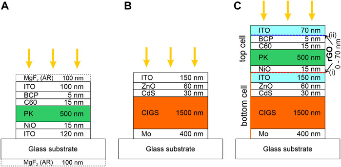
FIGURE 1. Schematic representation of fabricated single-junction (A) PK solar cell, (B) CIGS solar cell, and (C) tandem PK/CIGS cell. In the later one, the two positions of the introduced rGO layers are marked with dashed lines.
A single-junction CIGS cell, already designed for usage as a bottom cell in tandem structure, was also fabricated and used for calibration and verification of the optical model. Its schematic structure is presented in Figure 1B. An Mo back contact was deposited on a soda-lime glass (SLG) substrate, followed by an absorbing CIGS layer (with EG = 1.07 eV) as p-type material and thin CdS as an n-type material, forming the p–n solar cell junction. On the top side, the cell was contacted with thin ZnO followed by an ITO electrode in our case. A complete PK/CIGS tandem structure, as used in simulations, and the corresponding layer thicknesses are presented in a schematic cross-section in Figure 1C. The incorporation of thin rGO layers at positions (1) and (2) in the PK/CIGS structure is indicated.
2.3 Experimental
2.1.1 Experimental
In this article, commercially available graphene oxide (GO) flakes in an aqueous solution (Graphene Supermarket) are used and spray-coated onto glass substrates, which were heated at 100°C during the coating process. A Simcoat XYZ tabletop ultrasonic coating system with an ultrasonic spray nozzle of 120 kHz is used for the GO flakes deposition onto glass substrates. The liquid flow rate is kept constant at 0.5 ml/min and the air pressure is at 3 psi. Several layers were deposited by the spray-coating process to achieve the desirable GO layer thickness. The thickness of the GO layer was tuned to be 80 nm, measured by means of atomic force microscopy. For the laser reduction process, a KrF excimer nanosecond UV laser source (248 nm, 20 ns) was employed. In particular, the spray-coated GO layers on glass substrates were subjected to irradiation with a number of laser pulses of specific laser fluence in ambient conditions.
2.1.2 Perovskite Solar Cell Fabrication
The ITO-coated glass substrates (Colorado Concept Coatings LLC, ∼15 Ω/□) were cleaned sequentially in soap water, deionized water, acetone, and isopropyl alcohol in an ultrasonicator. 15 nm nickel oxide (NiOx) layer was deposited on ITO-coated substrates by linear magnetron sputtering. The perovskite precursor solution was prepared by dissolving CsI, FAI, FABr, and PbI2 in a mixed solvent of DMF:NMP to obtain Cs0.2FA0.8Pb (I0.947 Br0.053)3. The perovskite solution was blade-coated at room temperature. The obtained wet layer was then gas quenched with an N2 knife. Afterward, the film was annealed at 100°C for 30 min in an N2-filled glovebox. 15 nm Fullerene C60 and 5 nm BCP were thermally evaporated on perovskite film. Finally, 100 nm ITO was deposited by magnetron sputtering. 100 nm MgF2 was thermally evaporated as the antireflection coating either on the front side of the glass or on top of the ITO layer.
2.1.3 CIGS Solar Cell Fabrication
The CIGS layers are produced by TNO, a partner in Solliance. The CIGS absorber layers are fabricated using sputtered CuGa, and in layers on Mo/glass substrates and selenized in a Smit Oven (van der Vleuten et al., 2020). The CIGS absorber layers were then cleaned with ammonium sulfide [(NH4) S2] to etch undesired secondary phases. Subsequently, the CdS buffer layer was deposited at 60°C by chemical bath deposition. The CIGS layers are further finished into solar cells using sputtered i-ZnO/ITO window layers and sputtered Ni/Ag/Ni grids. The cells of 0.5 cm2 are manually scribed.
2.1.4 Characterization Methods
For GO-based samples the detailed measurements of wavelength-dependent optical transmission and reflection under different incident angles (0°, 35°, and 45°) for TE and TM polarization of light were performed using PerkinElmer LAMBDA 950 spectrophotometer, producing input data for the Nika software. Measurements of both, initial GO and rGO on glass substrates and on ITO coated substrates, were performed.
The EQE measurements were performed using a Bentham PVE300 spectral response setup with Halogen and Xenon lamps. The tool was calibrated with a Si reference cell and Ge cell for the NIR. The EQE spectra were recorded from 300 to 900 nm with the step of 5 nm for perovskite cells and from 300 to 1400 nm with a 10 nm step for the CIGS cells. The reflection was measured using an integrated sphere, and a calibration file for the reflection was used.
3 Results
3.1 Determination of Complex Refractive Indices of GO-Based Layers
The first step was to determine the optical properties of fabricated GO-based layers. Here, results of wavelength-dependent complex refractive indices of a GO film and a rGO film, both deposited on glass substrates, are presented. The rGO film was reduced upon irradiation with 50 UV laser pulses of 248 nm laser wavelength, 20 ns pulse duration, and laser fluence of 20 mJ/cm2. The thicknesses of the GO and the rGO layers were determined to be 70 and 57 nm, respectively. Both layers were deposited on a 1 mm thick glass substrate. Complex refractive indices were determined by the reflectance–reflectance method under different incident angles of the applied beam.
Real part (n) and the imaginary part extinction coefficient (k) of the extracted complex refractive indices for the initial GO and the reduced rGO are shown in Figures 2A,B, respectively. Results show that, in this case, the initial GO exhibits a bit higher refractive index, compared to the rGO layer. On the other hand, the extinction coefficient shows higher values for the characterized rGO, indicating higher absorption in this layer. Increased absorption due to the reduction process may be linked to increased carbon density as a result of the rGO volume reduction. The gradual increase of the absorption also suggests that electronic conjugation within the graphene sheets is restored while irradiating and reducing GO (Huang et al., 2011). In addition, during the reduction process, removal of oxygen-containing groups occurs. There is evidence that the oxygen-containing group is removed through the change of the GO layer transparency (coloration) after laser treatment. This can be attributed to a higher carbon density in the reduced material, due to oxygen group removal. The gradual increase in the absorption also suggests that electronic conjugation within the graphene sheets is restored while irradiating and reducing GO (Huang et al., 2011). Also, during the reduction process, removal of oxygen-containing groups occurs, which leads to the recovery of the π-network. The alteration of the refractive index value during the reduction process could also be attributed to the significant increase in the free carrier density. However, the laser reduction process allows further optimization of the optical and electrical properties of layers. In this article, we used the as-determined optical properties of the rGO layer when simulating the tandem device. Parasitic optical losses were analyzed and quantified inside the solar cell in order to indicate directions and need for further rGO optimizations.
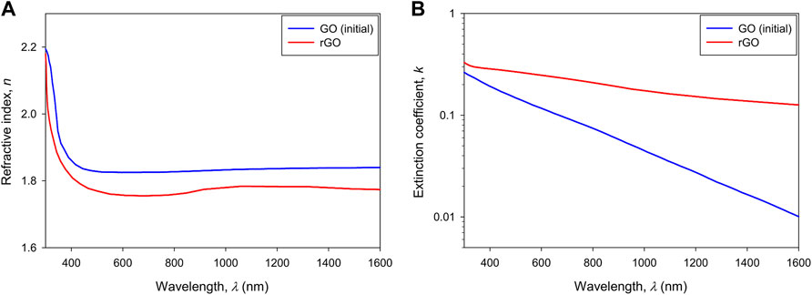
FIGURE 2. (A) Real part of refractive index and (B) imaginary part: extinction coefficient of an initial GO layer and a laser-treated rGO layer.
Complex refractive indices of other materials used in the tandem PK/CIGS solar cell have been also determined for realistic layers in CIGS cell by either reflectance–reflectance, reflectance–transmittance, or ellipsometry measurements, as published in (Kovacic et al., 2019). For PK cells, optical constants and thicknesses of the NiOx, PK, C60, BCP, and ITO layers were extracted by spectroscopic ellipsometry measurements using the J.A. Woollam RC2® ellipsometer.
3.2 Validation of Optical Model on Subcells
Before starting with the loss analysis and optimization of structures in relation to rGO in tandem devices, it is important to check the exact status of simulations with respect to obtained experimental results of the available current state solar cells. Here, the validation of optical simulator SunShine was done on single-junction cells used later as subcells in simulated tandem configuration, namely, PK cell and CIGS cell. Selected structure configurations for this investigation are given in Tables 1, 2 for the case of top semitransparent PK and bottom CIGS cells, respectively. Solar cell parameters of both fabricated cells can be found in Table 3. Relatively low-performance values, especially for the CIGS cell, can be attributed to, so far, the nonoptimized electrical and optical properties of devices. The fabricated cells are still from the early stage of optimization processes.
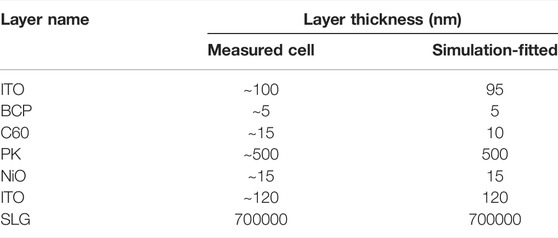
TABLE 1. The structure of the semitransparent PK cell with the thicknesses as set for fabrication and as fitted in optical simulations.
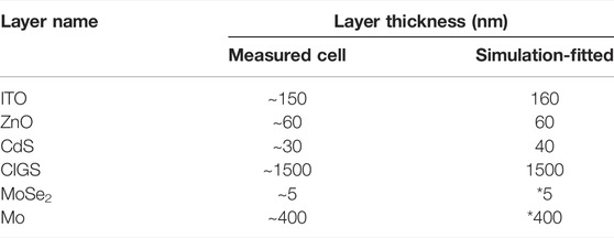
TABLE 2. The structure of the CIGS bottom cell with the thicknesses set for fabrication and as-fitted in optical simulations (*reduced back reflection).
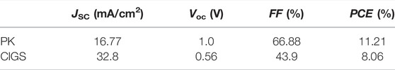
TABLE 3. Photovoltaic performance parameters of fabricated single-junction solar cells.
A comparison of measured and simulated EQEs is given in Figures 3A,B for the PK and CIGS cell, respectively. In general, relatively good matching between measurements and simulations can be observed for both cells. In simulations, only minor variation of layer thicknesses, well in the range of fabrication uncertainties, both for perovskite solar cell as well as CIGS solar cell, had to be performed to match the positions of interference fringes in wavelength-dependent characteristics. Detailed layer thicknesses as specified for fabrication and as determined by simulations are given in Tables 1 and 2 for PK and CIGS cells, respectively. In this case, the CIGS cell was simulated by considering the front random native roughness of ∼1500 nm thick CIGS film, with a value of σrms = 52 nm (Krc et al., 2005). This value was applied to all interfaces of layers on top of the CIGS absorber. Additional simulations reveal that roughness, in this case, has only minimal effect and is thus not considered in further simulations.
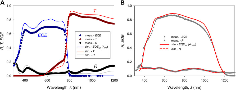
FIGURE 3. Measured EQE and simulated EQEopt, reflectance R, and transmittance T of (A) a semitransparent PK cell and (B) CIGS cell.
For the PK cell, simulated EQEopt shows higher values than the measured EQE. We attribute this variation to limited charge carrier extraction, as the developed PK recipe for semitransparent cell and the layers stack was not yet fully optimized in this case. Some deviations can be also observed in reflectance and transmittance curves, which can be contributed to the deviations of structures regarding the antireflection coatings. The EQE was measured for cells without added antireflection coatings (no MgF2 at back or front), while R and T were measured on devices with 100 nm MgF2 antireflection coatings at both, front and backside of the device.
For the CIGS cell, significantly reduced back reflection (reduced by 80% compared to the value calculated from refractive indices) had to be considered in simulations, indicating optically nonoptimized CIGS/Mo interface and Mo back contact in the case of these test cells. In case of better back reflection, an increase in long-wavelength reflectance and EQEopt is expected (Krc et al., 2017). In further simulations, reflectance of the CIGS/Mo interface was considered as expected from our previous experiments (including a thin MoSe2 interfacial layer in between, resulting in a ∼25% decrease in reflectance characteristics) (Lin et al., 2016 and Kovačič et al., 2019). Besides, nonperfect extraction of charge carriers from the CIGS absorber may be attributed to somewhat lower measured EQE compared to simulated EQEopt.
The results of validation and previous model applications (Kovacic et al., 2019 and Kovačič et al., 2019) present in our opinion a sufficient level of confidence in the models and input data to study the trends in single-junction and tandem PK/CIGS devices. In our optical study of tandem devices, we still consider an ideal extraction of charge carriers from absorber layers; thus, EQEopt can be compared to EQE.
3.3 Determination of Optical Losses in Tandem Cell Without rGO Layers
Tandem devices can be contacted via two terminals (2T), at the most front and most rear contact or intermediate terminal(s) can be used in 3- or 4-terminal (3T and 4T) devices, where each subcell in stacked configuration can be contacted individually. In the case of a 2T device, the subcell with minimal photocurrent determines the total current of the tandem cell due to a series of electrical connections. Thus, there exists a requirement of current matching to avoid the current losses. In the case of 3T or 4T, the photocurrents and voltages can be accessed individually and the restriction on current matching is not important anymore.
In the scope of further optical simulations, we detect short-circuit current densities, JSCopts, of the top and bottom cell individually; however, we consider the 2T configuration, where only the initial tandem cell without the rGO layers was approximately current matched. In further modifications of the cell (introduction of rGO layers), current matching has not been performed in this study (by tunning the PK layer thickness and bandgap) since our intention was to decouple and clearly indicate the effect of introduced rGOs on the performance of the individual subcell. For 2T device configuration, thus, the minimal JSC (corresponding either to the top or bottom subcell) has to be considered as JSC of the entire 2T tandem cell. In the final device, a further optimization process of current matching is required as well.
Initially, a detailed optical analysis of reflectance, transmittance, and absorptance in individual layers for tandem cells without introduced rGO layers was performed. The results of wavelength-dependent R, T, and A in individual layers are presented in Figure 4A. Absorbances of PK and CIGS active layers, corresponding to the EQEopt of the top and the bottom subcell, lead to the photocurrents, whereas A of other supporting layers is considered as parasitic losses with neglected contributions to the photocurrent. JSCopt values calculated from As by considering AM1.5g solar spectrum in the range from 300 to 1200 nm are presented in Figure 4B. Results show that absorbed light in active PK and CIGS layers contributes to JSCopt of 17.7 mA/cm2 and 17.0 mA/cm2 for the top and bottom subcell, respectively. Together, around 75% of incident light photons in the given wavelength range is converted to useful photocurrent, leaving 25% of light photons lost due to different optical loss channels.
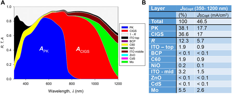
FIGURE 4. (A) Distinctive color sections represent a wavelength-dependent relative part of individual layer absorptances (A) - absorption, and reflectance-related loss presented by 1, reflectance (1—R) for the proposed tandem PK/CIGS solar cell (without rGO). Indicated are beneficial absorptances (APK and ACIGS), while other parts represent parasitic absorption losses in individual layers and reflection losses. (B) Distribution of JSCopt active contributions from PK and CIGS layers and losses in other layers in relative (%) and absolute values for the AM1.5 spectrum in the wavelength range of 350–1200 nm.
Results point towards relatively high reflectance as one of the main optical loss factors for both PK and CIGS cells in tandem configuration, contributing up to 12.3% of lost JSCopt. This loss can be decreased by applying antireflection films (e.g., MgF2) or additional microtextured light management foils to the device to trap long-wavelength light in the cell and increase the probability to be absorbed in active PK and CIGS layers (Jošt et al., 2017; Kovacic et al., 2019; and Kovačič et al., 2019).
For the top PK cell, the main optical losses are due to absorption in the top ITO and C60 layer, together contributing up to 3.8% of JSCopt losses in tandem.
For the bottom CIGS cell, main optical losses seem to be attributed to the poorly reflecting Mo back reflector, contributing up to 5.5% current loss. However, it should be noted that these losses occur in the wavelength range where photon energies are close or lower with respect to the selected CIGS bandgap. Therefore, by improving the back reflector of the cell with a 1500 nm thick CIGS absorber, only a part of reflected light can be absorbed in the CIGS layer, being rather reflected out of the device. Additional optical simulations of the hypothetical tandem device with ideally reflecting flat back contact would increase the JSCopt of the bottom cell by 0.7 mA/cm2 which is 4.1% relatively. Further analysis of the results shown in Figure 4 indicates that nonnegligible optical loss is also due to the ITO layer in the middle of the device, presenting up to 3.2% of JSCopt. Here, losses could be decreased by thinning down the layer or using an alternative solution at this recombination junction between subcells.
3.4 Analysis of Tandem PK/CIGS Structure With rGO Layers
The introduction of rGO layers at the two possible positions (see Figure 1C) is analyzed from the optical point of view. As mentioned, electrical simulations are not carried out in this article. The optical properties of the rGO layers as presented in Figure 2A and B are used in simulations. The thickness of rGO layers was selected as a variable parameter in simulations and was varied from 0 to 70 nm. Although in some applications very thin rGO films are used (less than 3 layers of material), we extend the research here to a much broader range of thicknesses (up to 70 nm) to achieve the best compromise between optical (transparency and low parasitic absorption) and electrical properties (conductivity and carrier recombination) of the layer in the PK/CIGS tandem devices.
Results of optical simulations of tandem PK/CIGS device with the rGO layer in the middle (1), at the top (2), and at both positions are presented in plots in Figure 5. In addition, rGO with the optical properties as determined in Figure 2, and a hypothetical case for optically idealized rGO with zero parasitic absorption (zero extinction coefficient) was included in simulations to quantify the theoretical optical potential of such interlayers. Optimization of the laser reduction process allows for the improvement of optical and electrical properties of layers. With the further tuning of the reduction process much lower absorption of rGO material should be achievable. In Figure 5, graphs on the left present the EQEopt and parasitic absorptance in the rGO layer. 1-R curves are added as well. Graphs on the right present the corresponding JSCopts as a function of rGO thickness.
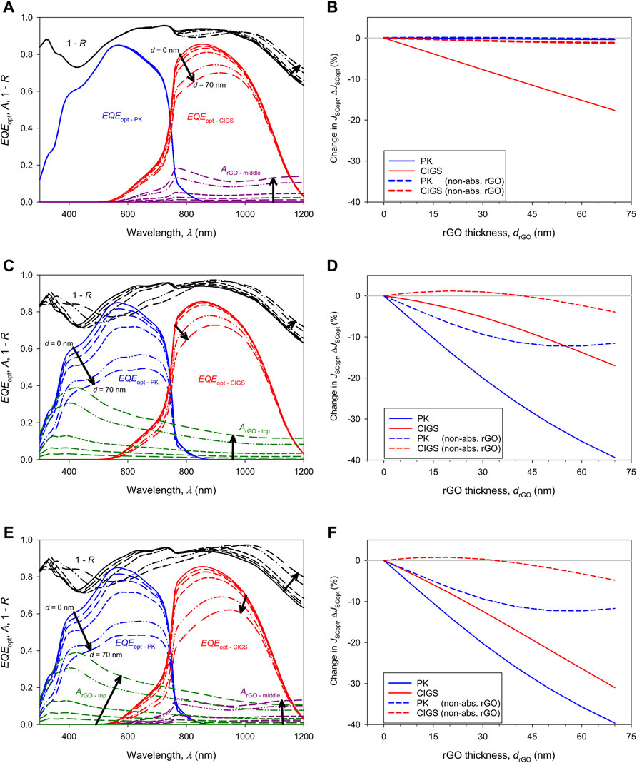
FIGURE 5. EQEopt, 1-R, and ArGO considering rGO layers at (A) middle position (1), (C) top position (2), (E) both positions (1) and (2) and corresponding JSCopt depending on thickness of introduced rGO layers (B), (D), and (F), respectively). Lines in (A), (C), and (E) correspond to rGO thickness of 0, 5, 10, 20, 50, and 70 nm following the sequence as indicated with the arrows.
Results show that the tandem cell with rGO at the middle position (1), has an impact on EQEopt of the bottom (CIGS) cell predominantly, while the top PK cell is almost not affected optically, see Figures 5A and B. Such a small effect on the PK top cell is expected in this case since the amount of incident light that passes the top PK cell is not affected and a negligible change in absorptance is associated with slightly changed reflectivity properties at the backside of the PK cell due to the introduced rGO layer (see discussion section). However, by the introduction of rGO and by increasing its thickness from 0 to 70 nm, EQEopt of the CIGS cell noticeably falls. This decrease is mainly attributed to the increased parasitic absorption in the thicker rGO layer. Focusing on 1-R curves, in the wavelength range λ = 800–900 nm, a decrease with the increased thickness or rGO layer is observed, whereas in the long-wavelength range (λ > 900 nm), the opposite trend occurs. The decrease in 1-R curves (increase in R) is due to increased parasitic absorption in the thicker rGO layer in this wavelength range, letting less light to leave the structure. The increase in 1-R curves at longer wavelengths (decrease in R) is attributed to interference effects due to introduced rGO as it will be addressed in the discussion by partial structure simulations.
The same trend as observed for absorptances of the active CIGS layer in Figure 5A is reflected in the JSCopt values of the CIGS cell (Figure 5B). For example, in a 5 nm thin rGO, a decrease in the JSCopt of the CIGS cell is around −1.3% and increases linearly with the increased thickness, according to simulations. For the idealized rGO with zero absorption, the JSCopt values stay almost unchanged as indicated by dashed lines in the plot.
Next, we analyze the results of simulations of the tandem cell with the rGO layer at top position 2), i.e., between the top ITO and BCP layer. Both EQEopt for PK and CIGS subcell shown in Figure 5C decrease with an increased rGO layer thickness in this case. This is since the rGO located at the top position absorbs short- and long-wavelength incident light prior to reaching both active layers (PK and CIGS). The corresponding JSCopt dependencies are plotted in Figure 5D. Again, almost linear decreases in JSCopts are observed for increased thickness of rGO. A higher rate of decrease is present in JSCopt of the PK cell. This is because rGO has a higher extinction coefficient and thus parasitic absorption in the short-wavelength range of light where the PK subcell is sensitive to light absorption. For a 5 nm thick rGO layer, JSCopts of the top and bottom cells are reduced by 3.5% and 0.6%, respectively. In this case, the requirement for using either very thin or low-absorbing rGO material (at short and long wavelengths) is even more important in the final optimization of the device. Simulation results of a hypothetical rGO layer without absorption losses show shallow interference effects in JSCopt dependency on rGO thickness, resulting in even slight improvement in JSCopt of the CIGS cell around the thickness of 20 nm.
The last study case includes rGO at both positions in the middle and at the top of the tandem cell [(1) and (2)]. Again, reduced EQEopt in both, PK and CIGS cells is observed (Figure 5E) and the corresponding JSCopts (Figure 5F). In both graphs, the values at the horizontal axis correspond to both rGOs (thickness variation of both rGOs simultaneously). As indicated before, the main restriction are parasitic optical losses, now in both rGOs, resulting in a cumulative reduction of JSCopt in the CIGS subcell. However, due to the higher extinction coefficient of rGO at shorter wavelengths, the losses in the PK subcell are higher. If both rGO layers are set to 5 nm, the corresponding decreases in JSCopts are 3.5% for the top PK and 1.9% for the bottom CIGS cell. Simulation results with hypothetical rGOs with zero absorption losses show a very similar trend as in the case study before.
4 Discussion
In the previous section, we pointed out and quantified optical losses related to introduced optically nonoptimized rGO layers in the PK/CIGS structure. The loss percentage in JSCopt for optically nonoptimized rGOs needs to be compensated by the FF and/or VOC improvement linked to the introduced rGO to achieve the gain in device performance already by using optically nonoptimized rGOs. Simulation results show that, from the optical (absorption loss) point of view, it is important to use the rGO layer as thin as possible. A detailed analysis of the electrical properties according to the rGO materials in combination with the presented optical analysis will reveal and quantify the actual benefits related to the introduced rGO layers. In any case, further optimization of optical properties of rGO materials is of high importance. Therefore, we performed further optical analysis to check optical potential related to idealized (hypothetical) cases in this section.
For this purpose, we analyze the optical situation in the partial internal structure around the introduced rGO layers. This analysis also contributes to a better understanding of the effects presented in previous sections. Here, we present simulation results for an isolated internal structure stack related to rGO position (1), namely, NiO/rGO/ITO. Reflectance into the incident medium (in this case NiO), absorptance in rGO, and transmittance into the outgoing medium (ITO) were simulated and analyzed. This additional analysis was motivated by the fact that the introduction of a new layer into the two adjacent ones affects (decreases or increases) the reflectivity properties of the stack, depending on the sequence of refractive indices of adjacent layers. While for the top position (2) of the introduced layer, reduced reflectance is desired for a broad wavelength range; for the middle position (1), increased reflectance for shorter wavelengths (to improve back reflectance of short-wavelength light to the top cell) and increased transmittance of long-wavelength light (to gain in optical absorption in CIGS) would be the optimal case. Results of simulations of R into NiO and T into the ITO layer are presented in Figure 6A,B, respectively, for two different rGO layer thicknesses (5 and 70 nm). In addition, beside rGO with complex refractive indices as presented in Figure 2, also an ideal case with nonabsorbing rGO, was considered in simulations again. Additionally, for both mentioned cases, the real part of refractive index (n) was changed by ‘+/−20% to detect possible improvements in reflectance/transmittance properties of the stack related to different n of rGO. Tuning of the n values of rGO is possible by proper control of the reduction process and by the timing of the laser irradiation parameters (such as fluency and exposure time). Please note the magnified scale for R in Figure 6A compared to the scale for T in Figure 6B.
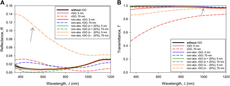
FIGURE 6. Simulated (A) R and (B) T of isolated internal structure stack NiO/rGO/ITO for the rGO intermediate position (1).
In the simulated NiO/rGO/ITO stack, the sequence of the corresponding n values (at λ = 550 nm) is 2.23/1.76/1.87. Thus, rGO with lower n compared to ITO and NiO introduces a high/low/(moderately) high sequence of n, giving the opportunity to affect the reflectance/transmittance properties of the stack. Simulations of structures with a 5 nm thick rGO layer reveal very similar behavior of R and T in Figure 6, regardless of the variation in rGO absorption properties or refractive index change. This was also observed in EQEopt and JSCopt results presented in the previous section (Figure 5) for the nonoptimized and nonabsorbing rGO case. However, going to thicker rGO, interference effects start to play a role in R and T characteristics. As already pointed out in the previous section, nonoptimized absorption properties of rGO hinder the behavior of the bottom CIGS cell, which is also reflected in the low T curve for the nonoptimized rGO with the thickness of 70 nm. However, considering 70 nm thick nonabsorbing rGO, with decreased n by 20%, the corresponding R and T curves reveal a direction towards the mentioned desired wavelength-dependent characteristics, increased R at shorter wavelengths to enhance back reflection to top PK cell and increased T at longer wavelengths to enable high transmission to the bottom CIGS cell (see grey arrows in Figure 6A and B). The decreased n of rGO increases the contrast in the high/lower n/(moderately) high refractive index stack. Without further optical optimization, the potential increase in JSCopt of the top PK due to the mentioned interference effect, simulated on the complete PK/CIGS cell level, is +0.8%, compared to the reference cell without rGO. The decrease of JSCopt in the bottom cell still stays at a relatively low level of −6.6%. A similar effect can be observed if increasing n of rGO by +20%. In this case interference effects for 70 nm thick rGO result in a JSCopt increase of 1.2% for the CIGS subcell, while the decrease in JSCopt of the PK subcell remains low at −0.6%. Thus, if achieving very low absorbing rGO layers with lower or higher n values at the same time, thicker interlayers might be of interest.
5 Conclusion
In the presented article, we carried out optical simulations to study optical effects related to the laser-treated (reduced) graphene oxide layers, rGOs, introduced at the top and middle position in the PK/CIGS tandem solar cells. First, complex refractive indices of initial, GO, and an rGO layer were determined and presented. Gained optical data served as a basis for further optical simulations and analysis of the complete tandem structure.
The quantification of optical losses in tandem device with rGOs indicates noticeable effects of parasitic absorption in rGO, which for thick (70 nm) optically nonoptimized rGO at the middle position brings over −17% decrease in Jsc of the CIGS subcell and even larger decrease when used at the top position with over −39% reduction in Jsc of the PK subcell. It is further shown that the usage of thin rGO layers (<5 nm) is beneficial in this case, as only a small decrease in Jsc of around 3.5% for the PK and even lower for the CIGS subcell is predicted. These small loss percentages in Jsc due to optically nonoptimized rGOs need to be compensated by the FF and/or VOC improvement to assure the gain in device performance.
Furthermore, optical analysis revealed potential related to idealized, nonabsorbing rGO. In this case, much lower losses in Jsc can be observed for both subcells. Additionally, for thicker nonabsorbing rGO, the interference effects in internal reflection and transmission start to play a role. For the case of 70 nm thick nonabsorbing rGO, with decreased n by –20%, results show the desired wavelength-dependent characteristics, increased R at shorter wavelengths, enhancing back reflection to top PK sub-cell, and increased T at longer wavelengths, supporting transmission to the bottom CIGS cell. This results in improved Jsc of PK subcell of 0.8% with only a slight decrease in Jsc of CIGS subcell. This indicates that, by further trimming the complex refractive index of introduced rGO layers, which might be achieved by the laser reduction process, additional positive interference effects could be achieved resulting in further improvements of Jsc of both PK and CIGS subcells related to optical properties of rGO.
Results indicate that, from the optical point of view, rGO absorption needs to be reduced, either by reduction of absorption coefficient or by using very thin rGO layers. In addition to, further research has to be focused on the optimization of rGO layers to establish improvements in electrical parameters (fill factor and/or open-circuit voltage) of the devices. In this regard, our work presents a guideline for optical requirements of rGOs and quantifies, based on the JSC changes, what improvements need to be achieved in the electrical optimization of rGO layers to be successfully deployed in PK/CIGS tandem devices.
Data Availability Statement
The original contributions presented in the study are included in the article/Supplementary Material, further inquiries can be directed to the corresponding author.
Author Contributions
MK performed optical simulations and optical characterization of rGO layers. MK and JK prepared the basic concept and first draft of the manuscript together with MAT. MAT and JK together with MK coordinated the activities of research and manuscript preparation. KS, SM, and ES, prepared rGO layers for optical characterization for the purpose of later integration in the tandem devices. MET, YK, JD, TA, and BV provided experimental results on PK and CIGS solar cells. They all contributed to the experimental parts of the manuscript. All authors contributed to manuscript revision, read, and approved the submitted version.
Funding
The authors acknowledge the financial support of the FLAG-ERA JTC 2019 LASERGRAPH project (reference no.: JTC-2019-013) and Slovenian Research Agency ARRS (P2-0415 and J2-1727). TNO, a partner in Solliance, is acknowledged for providing the CIGS absorber layers.
Conflict of Interest
The authors declare that the research was conducted in the absence of any commercial or financial relationships that could be construed as a potential conflict of interest.
Publisher’s Note
All claims expressed in this article are solely those of the authors and do not necessarily represent those of their affiliated organizations or those of the publisher, the editors and the reviewers. Any product that may be evaluated in this article, or claim that may be made by its manufacturer, is not guaranteed or endorsed by the publisher.
References
Al-Ashouri, A., Köhnen, E., Li, B., Magomedov, A., Hempel, H., Caprioglio, P., et al. (2020). Monolithic Perovskite/silicon Tandem Solar Cell with >29% Efficiency by Enhanced Hole Extraction. Science 370, 1300–1309. doi:10.1126/science.abd4016
Booth, H. (2010). Laser Processing in Industrial Solar Module Manufacturing. Jlmn 5, 183–191. doi:10.2961/jlmn.2010.03.0001
Čampa, A., Krč, J., Smole, F., and Topič, M. (2005). “Determination of Optical Constants of Thin Amorphous Silicon Films by Reflectance and Transmittance Measurements,” in 41th International Conference on Microelectronics, Devices and Materials and the Workshop on Green Electronics (Ribno, Slovenia: IEEE).
Čampa, A. (2012). NIKA - Model for Extracting Refractive Indices. Otočec, Slovenia: Laboratory of Photovoltaics and Optoelectronics.
Green, M. A., Dunlop, E. D., Hohl‐Ebinger, J., Yoshita, M., Kopidakis, N., and Hao, X. (2021). Solar Cell Efficiency Tables (Version 58). Prog. Photovolt. Res. Appl. 29, 657–667. doi:10.1002/pip.3444
Hawash, Z., Ono, L. K., and Qi, Y. (2018). Recent Advances in Spiro‐MeOTAD Hole Transport Material and its Applications in Organic-Inorganic Halide Perovskite Solar Cells. Adv. Mater. Inter. 5, 1700623. doi:10.1002/admi.201700623
Huang, L., Liu, Y., Ji, L.-C., Xie, Y.-Q., Wang, T., and Shi, W.-Z. (2011). Pulsed Laser Assisted Reduction of Graphene Oxide. Carbon 49, 2431–2436. doi:10.1016/j.carbon.2011.01.067
Jošt, M., Albrecht, S., Kegelmann, L., Wolff, C. M., Lang, F., Lipovšek, B., et al. (2017). Efficient Light Management by Textured Nanoimprinted Layers for Perovskite Solar Cells. ACS Photon. 4, 1232–1239. doi:10.1021/acsphotonics.7b00138
Jošt, M., Köhnen, E., Al-Ashouri, A., Bertram, T., Tomšič, Š., Magomedov, A., et al. (2022). Perovskite/CIGS Tandem Solar Cells: From Certified 24.2% toward 30% and beyond. ACS Energ. Lett 7, 1298–1307. doi:10.1021/acsenergylett.2c00274
Konios, D., Kakavelakis, G., Petridis, C., Savva, K., Stratakis, E., and Kymakis, E. (2016). Highly Efficient Organic Photovoltaic Devices Utilizing Work-Function Tuned Graphene Oxide Derivatives as the Anode and Cathode Charge Extraction Layers. J. Mater. Chem. A. 4, 1612–1623. doi:10.1039/C5TA09712F
Konios, D., Petridis, C., Kakavelakis, G., Sygletou, M., Savva, K., Stratakis, E., et al. (2015). Reduced Graphene Oxide Micromesh Electrodes for Large Area, Flexible, Organic Photovoltaic Devices. Adv. Funct. Mater. 25, 2213–2221. doi:10.1002/adfm.201404046
Konios, D., Stylianakis, M. M., Stratakis, E., and Kymakis, E. (2014). Dispersion Behaviour of Graphene Oxide and Reduced Graphene Oxide. J. Colloid Interf. Sci. 430, 108–112. doi:10.1016/j.jcis.2014.05.033
Kovačič, M., Krč, J., Lipovšek, B., Chen, W.-C., Edoff, M., Bolt, P. J., et al. (2019). Modelling Supported Design of Light Management Structures in Ultra-thin Cigs Photovoltaic Devices. Informacije MIDEM 49, 183–190. doi:10.33180/InfMIDEM2019.307
Kovacic, M., Krc, J., Lipovsek, B., Chen, W.-C., Edoff, M., Bolt, P. J., et al. (2019). Light Management Design in Ultra-thin Chalcopyrite Photovoltaic Devices by Employing Optical Modelling. Solar Energ. Mater. Solar Cell 200, 109933. doi:10.1016/j.solmat.2019.109933
Kr?, J., Smole, F., and Topi?, M. (2003). Analysis of Light Scattering in Amorphous Si:H Solar Cells by a One-Dimensional Semi-coherent Optical Model. Prog. Photovolt: Res. Appl. 11, 15–26. doi:10.1002/pip.460
Krc, J., Cernivec, G., Campa, A., Malmström, J., Edoff, M., Smole, F., et al. (2007). Optical and Electrical Modeling of Cu(In,Ga)Se2 Solar Cells. Opt. Quant Electron. 38, 1115–1123. doi:10.1007/s11082-006-9049-1
Krč, J., Lipovšek, B., and Topič, M. (2012). “Light Management in Thin-Film Solar Cell,” in Next Generation of Photovoltaics: New Concepts. Editors A. B. Cristóbal López, A. Martí Vega, and A. Luque López (Berlin, Heidelberg: Springer Berlin Heidelberg), 95–129. doi:10.1007/978-3-642-23369-2_4
Krc, J., Malmström, J., Smole, F., and Topic, M. (2005). “Determination of Light Scattering Properties of Cu(In, Ga)Se2 Films for Solar Cells,” in Proc 20th Eur. Photovolt. Sol. Energy Conf. (Springer), 1831–1834.
Krc, J., Sever, M., Campa, A., Lokar, Z., Lipovsek, B., and Topic, M. (2017). Optical Confinement in Chalcopyrite Based Solar Cells. Thin Solid Films 633, 193–201. doi:10.1016/j.tsf.2016.08.056
Krč, J., Smole, F., and Topič, M. (2002a). One-dimensional Semi-coherent Optical Model for Thin Film Solar Cells with Rough Interfaces. Inf. MIDEM 32, 6–13.
Krc, J., Topic, M., and Topic, M. (2016). Optical Modeling and Simulation of Thin-Film Photovoltaic Devices. Boca Raton, FL: CRC Press. doi:10.1201/b14551
Krč, J., Zeman, M., Smole, F., and Topič, M. (2002b). Optical Modeling Ofa-Si:H Solar Cells Deposited on Textured glass/SnO2 Substrates. J. Appl. Phys. 92, 749–755. doi:10.1063/1.1487910
Kymakis, E., Savva, K., Stylianakis, M. M., Fotakis, C., and Stratakis, E. (2013). Flexible Organic Photovoltaic Cells with In Situ Nonthermal Photoreduction of Spin-Coated Graphene Oxide Electrodes. Adv. Funct. Mater. 23, 2742–2749. doi:10.1002/adfm.201202713
Lang, F., Gluba, M. A., Albrecht, S., Rappich, J., Korte, L., Rech, B., et al. (2015). Perovskite Solar Cells with Large-Area CVD-Graphene for Tandem Solar Cells. J. Phys. Chem. Lett. 6, 2745–2750. doi:10.1021/acs.jpclett.5b01177
Lin, Y.-C., Hsieh, Y.-T., Lai, C.-M., and Hsu, H.-R. (2016). Impact of Mo Barrier Layer on the Formation of MoSe 2 in Cu(In,Ga)Se 2 Solar Cells. J. Alloys Comp. 661, 168–175. doi:10.1016/j.jallcom.2015.11.194
Liu, R., Qiu, R., Zou, T., Liu, C., Chen, J., Dai, Q., et al. (2018). SnO2-rGO Nanocomposite as an Efficient Electron Transport Layer for Stable Perovskite Solar Cells on AZO Substrate. Nanotechnology 30, 075202. doi:10.1088/1361-6528/aaf2ad
Maragkaki, S., Savva, K., and Stratakis, E. (2021). Advanced Photonic Processes for Photovoltaic, Energy Storage, and Environmental Systems. Adv. Sust. Syst. 5, 2000237. doi:10.1002/adsu.202000237
Min, H., Lee, D. Y., Kim, J., Kim, G., Lee, K. S., Kim, J., et al. (2021). Perovskite Solar Cells with Atomically Coherent Interlayers on SnO2 Electrodes. Nature 598, 444–450. doi:10.1038/s41586-021-03964-8
Petridis, C., Kakavelakis, G., and Kymakis, E. (2018). Renaissance of Graphene-Related Materials in Photovoltaics Due to the Emergence of Metal Halide Perovskite Solar Cells. Energy Environ. Sci. 11, 1030–1061. doi:10.1039/C7EE03620E
Schmid, M., Klenk, R., Lux-Steiner, M. C., Topič, M., and Krč, J. (2010). Modeling Plasmonic Scattering Combined with Thin-Film Optics. Nanotechnology 22, 025204. doi:10.1088/0957-4484/22/2/025204
Shockley, W., and Queisser, H. J. (1961). Detailed Balance Limit of Efficiency of P‐n Junction Solar Cells. J. Appl. Phys. 32, 510–519. doi:10.1063/1.1736034
Stratakis, E., Savva, K., Konios, D., Petridis, C., and Kymakis, E. (2014). Improving the Efficiency of Organic Photovoltaics by Tuning the Work Function of Graphene Oxide Hole Transporting Layers. Nanoscale 6, 6925–6931. doi:10.1039/C4NR01539H
Stylianakis, M. M., Sygletou, M., Savva, K., Kakavelakis, G., Kymakis, E., and Stratakis, E. (2015). Photochemical Synthesis of Solution-Processable Graphene Derivatives with Tunable Bandgaps for Organic Solar Cells. Adv. Opt. Mater. 3, 658–666. doi:10.1002/adom.201400450
Sugioka, K., and Cheng, Y. (2013). Ultrafast Laser Processing: From Micro- to Nanoscale Singapore: Routledge CRC Press. Available at: https://www.routledge.com/Ultrafast-Laser-Processing-From-Micro--to-Nanoscale/Sugioka-Cheng/p/book/9789814267335 (Accessed February 15, 2022).
Sygletou, M., Petridis, C., Kymakis, E., and Stratakis, E. (2017). Advanced Photonic Processes for Photovoltaic and Energy Storage Systems. Adv. Mater. 29, 1700335. doi:10.1002/adma.201700335
van der Vleuten, M., Theelen, M., Aninat, R., van der Werf, K., Mannetje, H. t., Reyes-Figueroa, P., et al. (2020). “Control over the Gallium Depth Profile in 30×30 cm2Sequentially Processed CIGS,” in 2020 47th IEEE Photovoltaic Specialists Conference, Calgary, AB, Canada (PVSC), 0640–0645. doi:10.1109/PVSC45281.2020.9300963
You, R., Liu, Y. Q., Hao, Y. L., Han, D. D., Zhang, Y. L., and You, Z. (2020). Laser Fabrication of Graphene‐Based Flexible Electronics. Adv. Mater. 32, 1901981. doi:10.1002/adma.201901981
Yu, Z., and Sun, L. (2015). Recent Progress on Hole-Transporting Materials for Emerging Organometal Halide Perovskite Solar Cells. Adv. Energ. Mater. 5, 1500213. doi:10.1002/aenm.201500213
Keywords: perovskite, CIGS, graphene oxide, optical simulation, tandem
Citation: Kovačič M, Krč J, Savva K, Maragkaki S, Stratakis E, Rashid M, Tutundzic M, Kuang Y, de Wild J, Aernouts T, Vermang B and Topič M (2022) Optical Simulation Study of Perovskite/CIGS Tandem Solar Cells With Reduced Graphene Oxide Layers. Front. Photonics 3:888486. doi: 10.3389/fphot.2022.888486
Received: 02 March 2022; Accepted: 06 April 2022;
Published: 04 May 2022.
Edited by:
Jianyu Yuan, Soochow University, ChinaReviewed by:
Qian Zhao, Nankai University, ChinaYong Peng, Wuhan University of Technology, China
Xufeng Ling, Chongqing University, China
Copyright © 2022 Kovačič, Krč, Savva, Maragkaki, Stratakis, Rashid, Tutundzic, Kuang, de Wild, Aernouts, Vermang and Topič. This is an open-access article distributed under the terms of the Creative Commons Attribution License (CC BY). The use, distribution or reproduction in other forums is permitted, provided the original author(s) and the copyright owner(s) are credited and that the original publication in this journal is cited, in accordance with accepted academic practice. No use, distribution or reproduction is permitted which does not comply with these terms.
*Correspondence: Milan Kovačič, bWlsYW4ua292YWNpY0BmZS51bmktbGouc2k=