 Jonas Mensing
 Wilfred G. van der Wiel
 Andreas Heuer
- 1Theory of Complex Systems Group, Institute of Physical Chemistry, University of Münster, Münster, Germany
- 2NanoElectronics Group, MESA+ Institute for Nanotechnology, Center for Brain-Inspired Nano Systems (BRAINS), University of Twente, Enschede, Netherlands
- 3Institute of Physics, Unversity of Münster, Münster, Germany
Nanoparticles interconnected by insulating organic molecules exhibit nonlinear switching behavior at low temperatures. By assembling these switches into a network and manipulating charge transport dynamics through surrounding electrodes, the network can be reconfigurably functionalized to act as any Boolean logic gate. This work introduces a kinetic Monte Carlo-based simulation tool, applying established principles of single electronics to model charge transport dynamics in nanoparticle networks. We functionalize nanoparticle networks as Boolean logic gates and assess their quality using a fitness function. Based on the definition of fitness, we derive new metrics to quantify essential nonlinear properties of the network, including negative differential resistance and nonlinear separability. These nonlinear properties are crucial not only for functionalizing the network as Boolean logic gates but also when our networks are functionalized for brain-inspired computing applications in the future. We address fundamental questions about the dependence of fitness and nonlinear properties on system size, number of surrounding electrodes, and electrode positioning. We assert the overall benefit of having more electrodes, with proximity to the network’s output being pivotal for functionality and nonlinearity. Additionally, we demonstrate an optimal system size and argue for breaking symmetry in electrode positioning to favor nonlinear properties.
1 Introduction
Brain-inspired computing represents an approach to advancing computation in machine learning applications by emulating the information processing of biological neural networks (Schuman et al., 2017). Compared to von-Neumann computing, it leverages massively parallel operation without separating memory and processing (Schuman et al., 2022). The implementation of these brain-like infrastructures aim to overcome limitations of traditional hardware and ultimately reduce energy consumption of current machine learning applications (Markov, 2014; Nakajima, 2020).
Nanoparticle (NP) networks as one example of physical systems (Dale et al., 2021; Milano et al., 2023) offer a promising avenue in this field. One current approach uses percolating scale-free NP networks with small-world properties (Fostner and Brown, 2015; Bose et al., 2017; 2019; Daniels et al., 2023; Mallinson et al., 2023). The intrinsic architecture of these networks includes conductivity dynamics which are crucial for computational tasks (Deng and Zhang, 2007; Kawai et al., 2019). Tunnel gaps forming between adjacent areas or clusters of nanoparticles act as nonlinear units or memristors, with their resistance exhibiting nonlinear responses to alterations in conductance. While the origin of the nonlinearity here arises from the connections of large clusters of NPs and not the particles themselves (Daniels et al., 2023), our approach is different.
Our research in this domain centers on single electronics within gold NP networks (Likharev, 1999; Durrani, 2003). Each NP serves as a conductive island, tunnel-coupled with its neighboring NP by an insulating organic molecule. When a NP is charged, its excess charges can tunnel to an adjacent NP only when the potential difference between them surpasses the repelling force exerted by the Coulomb energy. This Coulomb blockade effect imbues the charge tunneling dynamics in between NPs with a nonlinear activation function (van der Wiel et al., 2002).
The network is surrounded by electrodes, which serve as network inputs, outputs or controls (see Figure 1). The latter manipulate the network’s potential landscape and its charge tunneling dynamics, enabling the mapping of various functionalities to the input and output electrodes. Previous research has demonstrated the network’s input to output dependence to reconfigurably function as any type of Boolean logic gate when applying suitable control electrode voltages (Bose et al., 2015; Greff et al., 2016). Figure 1 shows a circuit diagram of a small NP network and electrode setup.
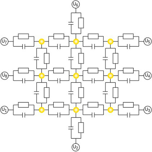
Figure 1. Circuit diagram of a gold nanoparticle network. Single nanoparticles (golden dots) are tunnel-coupled with each other by organic insulators. The network represents a regular-grid like connection topology. A NP-NP connection is represented by a capacitor and resistor in parallel. The network is placed on a highly doped Si substrate with an insulating SiO2 top-layer (not shown). The nanoparticles are surrounded by 8 Ti/Au electrodes applying voltages U1, …U8.
The integration of theoretical frameworks and simulation methods is of key importance in order to enable a closer understanding and subsequent optimization of these systems. In this paper, we use a kinetic Monte Carlo (KMC) approach to simulate electronic charge tunneling dynamics within the NP network. Prior research has already demonstrated the effectiveness of the KMC approach for studying single electronics devices (Kirihara et al., 1994; Wasshuber et al., 1997; Lee et al., 2008; Elabd et al., 2012). In particular, Van Damme et al. (van Damme et al., 2016) configured small networks of 16 nanoparticles to act as any Boolean logic gate. Although also smaller networks of just single NPs combined with electrostatic gates already show complex behavior such as XOR dependence for single realizations of voltages Yutaka Majima et al. (2017), our work extend these previous analyses by a comprehensive statistical investigation in several directions. First, it addresses the influence of system size (number of NPs) as well as the number and location of electrodes to optimize the chance to observe Boolean logic functionality. This information is relevant for the future design of such NP networks. Second, from a methodological perspective we introduce quantitative indicators for negative differential resistance and nonlinear separability. These nonlinear properties are imperative for a broad spectrum of brain-inspired computing (Yi et al., 2018) and machine learning applications (Elizondo, 2006). Here, we explicitly show that these indicators are quantitatively related to the ability of the network to display Boolean logic functionality. Third, due to the availability of fast array-based computations we highlight the efficiency of the implementation of the KMC approach.
2 Theory and methods
2.1 Nanoparticle networks
In this section, we first describe some fundamentals of the NP network design of (Bose et al., 2015) which served as a starting point for our work on this simulation tool. We then go through the electrostatic properties of the network and describe the dynamics of single-electron tunneling.
2.1.1 Electrostatics
The system of (Bose et al., 2015) consists of about 100 single Au NPs (20 nm diameter) which are interconnected by 1-octanethiols as an insulating organic molecule. The network is placed on a highly doped Si substrate with an insulting SiO2 top-layer and is surrounded by 8 Ti/Au electrodes.
From an electrostatic point of view, we just speak of a network of conductive islands interconnected by resistors and capacitors in parallel. Electrodes are understood as voltage sources UE. Figure 1 shows a circuit diagram of a 9-NP network in a regular grid-like connection topology.
We derive the capacitance values of the network using the image charge method (see Supplementary Section S1). The capacitance Cij between island i and j depends on the NP radii ri, rj, the distance between both NPs dij and the permittivity of the insulating material ϵm. The self capacitance Ci,self for the isolated island i close to the SiO2 layer depends on its radius ri and the permittivity of the insulating environment
For a given connection topology, we define the capacitance matrix C where diagonal components (C)ii represent the sum of all capacitance values attached to NP i and its self capacitance, while off-diagonal components (C)ij represent the cross capacitance in between NP i and j. In this work, we will not cover the impact of having variable connection topologies. Therefore, for all results we align NP in a regular grid like two-dimensional topology, such as in Figure 1, to isolate the upcoming results from additional disorder effects. Although we measure deviations in our system from the experiment due to the absence of disorder, still the overall statistical trends remain consistent (see Supplementary Section S4). Furthermore, the general statistical concepts to characterize non-linear behavior in the present type of systems are sufficiently general to be applied to the disordered case as well. Finally, it should be stressed that due to the generally different choice of control voltages, the overall system is not fully symmetric even for a symmetric network.
2.1.2 Single-electron tunneling
The network consists of conductive NPs interconnected by insulating molecules. The insulating molecules serve as tunnel barriers and functionalize the network. Excess charges residing on NP i tunnel to an adjacent NP j if their associated potential ϕi exceeds the repelling force resulting from the Coulomb energy
We define the network state
with C−1 as the inverse of the capacitance matrix. The internal electrostatic energy is described as
When voltages are applied to the surrounding electrodes, charges either enter the network or getting drained from it. The Helmholtz free energy determines the tunneling process and consists of the difference of total energy stored inside the network E and work W done by external electrodes
In its current state, the network will enter its next state associated to a change in free energy, either by a charge tunneling event from NP i to j
or by a charge tunneling event from NP i to electrode E
with elementary charge e. The change in free energy caused by a tunnel event serves as a measure of probability for this specific event with tunnel rate
where Rij denotes the resistance for jump path i → j and T the network’s temperature. If we apply constant voltages to all electrodes and execute around 10,000 charge tunneling events, the network will eventually settle in an equilibrium with constant electric currents entering or exiting the system via the electrodes. In this work we will not distinguish between charge tunneling events in between nanoparticles or in between nanoparticles and electrodes except for the above difference in free energy. We argue that this is a fair approximation, as also in the experimental situation the tunnel barrier with the electrodes is formed by an insulating layer of molecules.
We revisit Eq. 6 and see that increasing the network’s temperature T leads to drastically larger rates. Then, differences in the potential landscape are negligible and thermal excitation will be the dominant factor for the charge tunneling through the network. Overall, the device looses its functionality due to the linearization of the charge tunneling dynamics, i.e., its nonlinear activation functions (see Supplementary Section S2; Supplementary Figure S2). Therefore, we have to choose the temperature, so that condition EC > kBT is true. In this work we will stick to a temperature value of T = 0.28 K as in (Bose et al., 2015) which easily satisfies the latter condition with kBT ≈ 2.5 ⋅ 10–2 meV much smaller than the maximum charging energy of E ≈ 16 meV.
Additionally we also want to neglect coherent quantum processes, i.e., co-tunneling. For this we have to choose the tunneling resistance Rij in between NPs to be much higher than the quantum resistance of
2.2 Modelling and simulation
Based on the findings in the previous section, we explain how to build a KMC simulation tool to model the charge tunneling dynamics in NP networks. We also explain how to configure the network to mimic Boolean logic gates. In the main part of this project we focus on the six fundamental Boolean logic gates AND, OR, XOR, NAND, NOR, and XNOR. However we also show in Supplementary Figure S4 and argue in Supplementary Section S4 that our networks are able to function as any of the 16 two-input Boolean logic functions. In the last part we define the fitness value as a way to evaluate the quality of the network behaving as a particular Boolean logic gate. Based on this quality factor we derive QNDR and QNLS as new quantities to measure the properties of negative differential resistance (NDR) and nonlinear separability (NLS).
2.2.1 Kinetic Monte Carlo method
For a given network topology of NNP nanoparticles, initialized capacitance matrix C and set of electrode voltages UE, we firstly initialize the network’s state
In the next step we compute the cumulative distribution function (CDF) of all tunnel rates CDFΓ(n). The CDF consists of NT steps, one for each charge tunneling event n with its last step CDFΓ(n = NT) as the total rate constant ktot. Now, for the KMC procedure we first need to sample two random numbers x1 and x2 and find n where
As n was selected, we execute its corresponding charge tunneling event from NP i to NP j. This will leave the current state
Since only two elements of the state vector have been updated, for the next potential landscape we can just evaluate
where
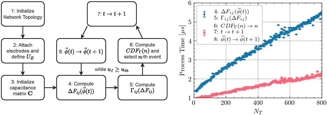
Figure 2. Using the different KMC steps shown in the flow shart, the process time is shown for steps 4-5 (tunneling events, blue curve) and steps 6-8 (advancing to the next step by selecting an event, red curve).
2.2.2 Computing functionalities
In this paper we want to investigate computing functionalities in the form of Boolean logic gates as a systematic property of the NP network. For Boolean logic we need two inputs and one output. Inputs, either set on/1 or off/0, produce an output signal depending on the underlying logic operation.
In our case, two electrodes will always serve as input electrodes. These electrodes are set to UI ∈ {0.0, 10.0} mV. Accordingly, there is an output electrode, which is always grounded, thus UO = 0.0 V. At the output we will measure the electric current
It enters the time t passed in the KMC procedure and the number of elementary charge jumps from network to output NNet→O and from output to network NO→Net. All other electrodes are called control electrodes with voltages set inside a range of UC ∈ [−50.0, 50.0] mV. The system’s phase space is spanned by NC electrodes with each point in phase representing a set of four different electric currents (I00, I10, I01, I11) corresponding to the four possible input electrode voltage combinations.
When increasing the network size, the electrode voltages drop across an increasing amount of NPs. To ensure comparable results, we scale the voltages of control and input electrodes to prevent the electric current at the output electrode from simply converging to zero as the network expands. To achieve this, we conducted simulations to assess the dependencies between input electrode voltage and output electrode electric current (I-V curves) across multiple systems. Through this analysis, we derived a scaling factor that maintains the electric current at a consistent level when multiplied by the initial voltage value, see Supplementary Section S3; Supplementary Figure S3.
Summarizing the simulation procedure, we first initialize a network of regular grid-like topology, electrode positions and electrostatics. Then we apply constant voltages to all electrodes and evolve the system into its equilibrium state. Afterwards, we start to track the times and the number of charge jumps exiting and entering the system via the grounded output electrode. This allows us to compute the electric current I and its relative uncertainty uI. The simulation ends when the KMC procedure reaches uI = 5% uncertainty or when ten million charge tunneling events have been executed.
2.2.3 Analysis methods
For a single simulation run, we sample 20,000 different control combinations, resulting in a set of four electric currents (I00, I10, I01, I11) for each combination, totaling 80,000 currents. To characterize nonlinear properties we introduce the three parameters
Ml/Mr signify the increase in output current upon altering the first/second input voltage, whereas X quantifies the cross-correlation between the two input voltages. In qualitative terms, Ml and Mr can be interpreted as an effective mobility of the output current concerning one of the two input voltages, while X denotes a measure of nonlinear coupling between both inputs.
Our objective is to evaluate the network’s ability to be configured into each Boolean logic gate using the fitness function
as a quality metric for the accuracy with which a given set of currents (I00, I10, I01, I11) represents a specific gate (Bose et al., 2015). The fitness comprises the slope or signal m, the mean squared error or noise MSE, and the absolute offset |c|. The signal is defined as
For δ = 0 we can exactly rewrite Eq. 12 for the individual gates in form of the quantities introduced in Eq. 11
Our goal is to estimate the first and second moment of the fitness distribution for each gate in terms of the statistical properties of Ml, Mr, and X. For this purpose we use two approximations: Firstly, we approximate
Using these approximations, for the AND, OR, NAND, and NOR gates we can write
and for the XOR and XNOR gates
Nonlinear behavior is in particular relevant for the NAND, NOR, XOR, and XNOR gates. For these gates we want to define measures which reflect the likelihood to find gates with sufficiently high fitness. For the NAND/NOR gates we consider the ratio
In the last step we have neglected the Pearson correlation between Ml and Mr.
The properties of the tanh-function mathematically restrict QNDR to values between 0 and 1. Since ⟨M⟩ is always positive, the actual upper bound is 0.5. For values of QNDR close to zero, the possibility of NAND and NOR gates is very small. Qualitatively, this measure allows us to assess the nonlinear feature of NDR required to achieve NAND/NOR gates.
A second statistical access to Eq. 16 is based on the fact that exactly for negative M NDR becomes visible in the input-output dependence. Therefore, when sampling many M values with corresponding probability density p(M), the integral
We mention in passing that the variance in Eq. 14 becomes larger for stronger correlations between Ml and Mr. This increases the probability to find gates (AND, OR, NAND, NOR) with higher fitness values.
From Eq. 15 we may conclude that XOR and XNOR gates have the same statistical properties. Since in this case the likelihood to find well-performing exclusive gates with high fitness values is directly related to the size of the variance of the fitness distribution, we can introduce
as a general measure for nonlinear separability (NLS), strongly reflecting the size of the nonlinear coupling X between both inputs.
In Supplementary Section S5, we generalize the approach described in this section towards systems of arbitrary numbers of inputs. However, for the sake of simplicity and as this work only covers two-input devices we will stick to the quantities of Eqs 11, 16, 17.
3 Results
In our study of nanoparticle networks manipulated by surrounding electrodes, key design features include the number of nanoparticles (NNP) and the location and quantity of control electrodes (NC). Although we find any possible two-input Boolean logic function in the sampled phase space (see Supplementary Section S4), here we just focus on the six major Boolean logic gates AND, OR, XOR, NAND, NOR, and XNOR. In this section, we first analyze the dependence of logic gate fitness (F) on the location and number of control electrodes. Given the significant impact of electrode positioning, the subsequent section addresses an increase in system size while considering two distinct electrode positioning setups. All results are contextualized within the framework of nonlinear properties. Additional insights into parameter dependence on NNP and NC can be found in Supplementary Section S7; Supplementary Figure S8.
3.1 Number and positioning of control electrodes
In this section, we explore the impact of the number of control electrodes and their positioning on network functionality, focusing on regular grid-like networks as discussed in Section 2.1.1. We use a 7 × 7 grid of NPs (NNP = 49) with one output and two input electrodes. To ensure that the majority of the system resides between input and output, we connect the output to a corner NP, and both inputs to the opposite edges.
We start by adding control electrodes near both inputs as we move closer to the output. These simulations are denoted ANC, where NC represents the number of controls. Subsequently, controls are removed from the system, starting with those near both inputs. These simulations are denoted BNC. The upper sketches in Figure 3 illustrate these simulated systems. This procedure allows us to study the effect on network functionality for varying control numbers and control positioning.
Figure 3. (A) Box plots of fitness values for all logic gates for networks with varying numbers of control electrodes. The length of a bar is equal to two standard deviations. Each box corresponds to one of the network diagrams shown above. The networks are projected along the x-axis in first ascending and then descending order of control electrode numbers. (B) Measure of negative differential resistance (QNDR), nonlinear separability (QNLS), and Pearson correlation corr (Ml, Mr) across variable numbers of control electrodes.
For each network, we sample 20,000 control voltage combinations, producing 20,000 sets of electric currents (I00, I10, I01, I11) using KMC. Utilizing Eq. 12, we calculate the fitness of each control voltage combination for each Boolean logic gate at δ = 0. The fitness distributions for each gate across different networks are depicted as box plots in Figure 3A, providing insights into the relationship between functionality and number of control electrodes.
First, in agreement with theoretical expectation, see Eqs 14, 15, we observe similar distributions for the respective AND/OR, NAND/NOR, and XOR/XNOR pairs. Furthermore, the distributions of the first two pairs are just mirror images of each other. Any remaining variations in
The impact on fitness when altering the number or position of control electrodes is significantly pronounced. We observe the most dramatic effect for controls in close proximity to the output electrode. The measures of nonlinear behavior, i.e., QNDR and QNLS, exhibit much larger values, see Figure 3B. Theoretically, one expects a strong correlation between QNDR and the availability of high-fitness NAND/NOR gates as well as between QNLS and the number of exclusive gates XOR/XNOR. Indeed, as seen from the box plots, a significant correlation is indeed observed.
As a secondary effect, it turns out to be helpful to use the maximum number of control electrodes NC = 9. Only in the case of AND/OR gates, a reduction in the number of controls generally leads to an increase in average fitness, while retaining electrodes near the output results in the most significant second moment.
Moreover, we observe a strong impact on the correlation coefficient between Ml and Mr. The presence of control electrodes adjacent to the output electrode as well as an increase in the number of control electrodes significantly reduces this correlation, going along with a stronger independence of I01 and I10.
As the results in Figure 3 suggest a substantial impact of the positioning of controls relative to the output or inputs, we performed two additional simulations for a network of size 7 × 7 as skechted in Figure 4A. First, we randomly adjusted the voltages of all seven electrodes and determined the resulting correlation between individual voltages and the output current. The Pearson correlations are illustrated in Figure 4B. In alignment with previous observations, electrodes in close proximity to the output electrode (specifically E5/E6) exhibit a strong impact via notable correlations between electrode voltages and output electric current I. This observation is further supported by the current-voltage dependencies, which are strongest when altering electrode voltages near the output (see Supplementary Figure S2).
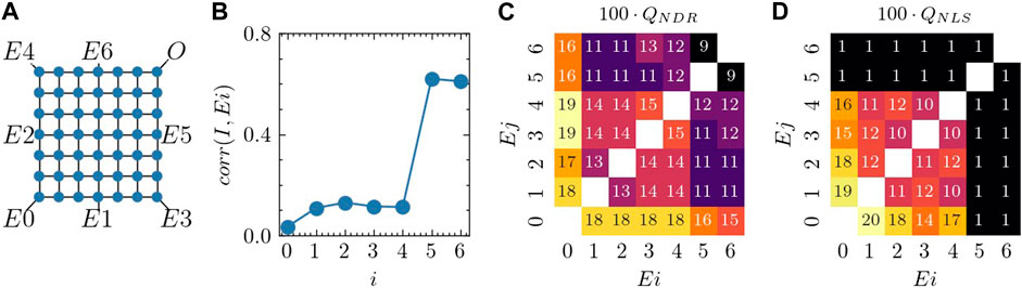
Figure 4. Influence of input electrode positions. (A) The graph depicts the simulated network. For every electrode combination (Ei, Ej), we examine four scenarios (Ei, Ej), (Ei + Δ, Ej), (Ei, Ej + Δ), (Ei + Δ, Ej + Δ). (B) The figures show current-voltage correlation, (C) negative differential resistance (NDR), and (D) nonlinear separability (NLS). To display the matrix values as integers in (C,D), each cell is scaled by a factor of 100.
In Supplementary Section S8; Supplementary Figure S9 we further study the charge tunneling behavior in a 1D system of NPs in two control electrode configurations. The first attaches the control electrode in the middle of the 1D string while the second attaches the control electrode in close proximity to the output. In the second setup we detect much stronger variation in the input electrode voltage regime associated to the Coulomb Blockade. Here we argue, that electrodes in close proximity to the output contribute most to the overall tunability of the network’s functionality as those electrodes primarily contribute to the manipulation of the potential landscape at the output region.
Second, we selected inputs at all possible electrode combinations (Ei, Ej) and sampled multiple control voltage combinations for any possible input electrode voltage combination {(Ei, Ej), (Ei + Δ, Ej), (Ei, Ej + Δ), (Ei + Δ, Ej + Δ)} with Δ = 10 mV. Figures 4C, D depict the nonlinear features of NDR and NLS, respectively, for each input position combination. If a single input is positioned adjacent to the output at E5 or E6, NLS is lost entirely due to the strong correlation with the electric current. For either NDR or NLS, optimal results are achieved by breaking symmetry and attaching one electrode at the corner opposite to the output electrode at position E0, with the second input placed elsewhere. In fact, there is not a significant difference in attaching the second input at E1, E2, E3, or E4. The advantage of having an asymmetric electrode connection may indicate a potential functionality gain for disordered networks in general.
3.2 System size
In this section, we investigate the influence of system size on the network functionality of regular grid-like NP networks. Following the experimental device proposed in (Bose et al., 2015), each network is surrounded by a configuration of eight electrodes. We connect the output to one corner of the network, and both inputs to the opposite edges to ensure that most NPs are between the input and output. This leaves five control electrodes to be attached at the remaining corners or edges.
Considering the strong relation to electrode positioning indicated in the previous section, we distinguish between two setups, as displayed in Figure 5A. In Setup A, we maintain consistent relative distances between all electrodes, connecting them either to a network corner or to the center of a network edge. In Setup B, the two electrodes, adjacent to the output, keep this minimum distance independent of system size.
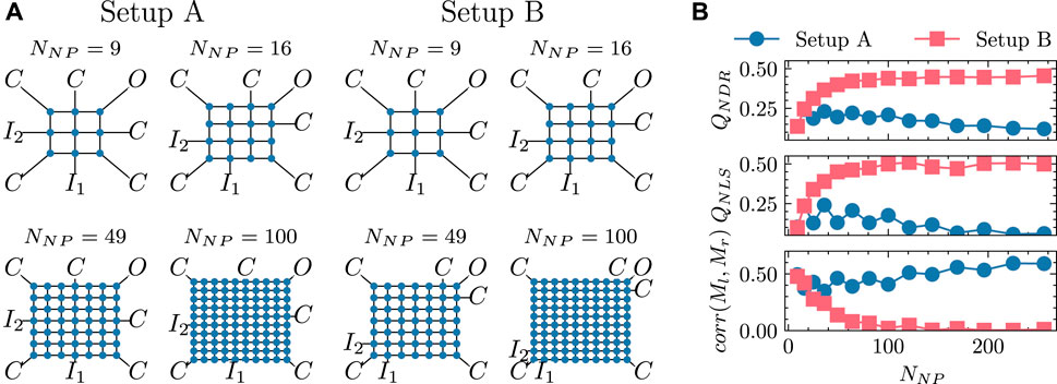
Figure 5. Simulation results for negative differential resistance (QNDR), nonlinear separability (QNLS), and input mobility correlation (corr (Ml, Mr)) in networks with varying numbers of NPs (NNP). These networks are surrounded by five control electrodes (C), two input electrodes (I1, I2), and one output electrode (O). Two setups are considered: Setup (A) maintains same relative distances between all electrodes, while Setup (B) keeps the electrodes at fixed positions.
Each simulation covers a specific system size, ranging from a 3 × 3 grid of NPs (NNP = 9) to a 16 × 16 grid of NPs (NNP = 256). We conduct 20,000 simulations for each system size, sampling control voltage combinations and producing sets of electric currents (I00, I10, I01, I11).
In Figure 5B, we break down the fitness into its key nonlinear components: QNDR, QNLS, and corr (Ml, Mr). There is a noticeable difference between both setups. In Setup B, a saturation behavior is observed for each nonlinear component. For NNP > 100, maximum NDR and NLS are achieved, and both inputs start to become fully independent. In fact, QNDR even reaches its theoretical upper bound QNDR = 0.5 as described in Section 2.2.3. In contrast, Setup A shows a less pronounced dependence. For systems seeking nonlinear separability, those with more than 50 NPs are not preferred. There is a decline in performance for increasing numbers of NPs, suggesting that smaller systems tend to perform better in terms of nonlinear features, provided there is a minimum of about 16 NPs. Regarding the correlation between both mobility values Ml and Mr, we observe that independence between input electrodes is never achieved, with corr (Ml, Mr) ≈ 0.5 for all networks. As shown in Supplementary Section S6; Supplementary Figure S5 the fitness distributions for AND, NAND, and XOR follow the same trend.
Similar to the findings in the previous section, we observe that control electrodes in close proximity to the output electrode play a pivotal role in overall network functionalities, particularly in terms of nonlinearity. As the system size increases in Setup A, the distance between the output and its closest control electrodes also increases, leading to a negative impact on performance. Despite achieving better results in larger systems with Setup B, it is crucial to note that in practical experiments, the network configuration may not resemble Setup B. Therefore, we argue that in experiments, one should be cautious about making the network too large, even though theoretically, saturation in nonlinearity should occur. Optimal results are obtained when aiming for a maximum of about NNP = 100, especially if electrodes can be densely packed. Otherwise, even a smaller system may prove to be more beneficial.
It is noteworthy that the saturation observed in Figure 5 occurs only for δ = 0, as QNDR and QNLS have been derived under this assumption (see Section 2.2.3). For larger values of δ, indicating a contribution of the logic gates offsets to the fitness value, we deviate from the saturation behavior, showing a clear maximum in fitness at about NNP = 100. Considering the preference for logic gates without an offset in the experimental setup, this observation further supports the identification of an optimal system size at or below 100 NPs.
4 Conclusion
We have developed a versatile and efficient kinetic Monte Carlo simulation tool designed to model charge tunneling dynamics in NP networks. Building upon established concepts of single electronics, the model has been specifically tailored for NP networks. The tool allows for the investigation of larger networks, comprising hundreds of NPs, within reasonable processing times.
Within our simulation framework, electrodes can be connected to the network at arbitrary positions and designated as input, output, or control electrodes. We have successfully mapped Boolean logic gate functionality to the dependence between input and output electrodes. Adjusting the control electrode voltages, the charge tunneling dynamics is manipulated, enabling the same network to be configured into any desired logic gate.
We assessed the quality of the network in functioning as a logic gate through a fitness function. Increasing the number of control electrodes consistently enhances fitness, with controls in close proximity to the output electrode proving most pivotal. When altering the positions of inputs and controls, our results demonstrated a loss of functionality when inputs are positioned in close proximity to the output. Additionally, we observed that an asymmetric connection of inputs could be advantageous.
We further related the fitness of each logic gate to a novel set of variables, enabling the derivation of measurement tools for key qualitative nonlinear features such as negative differential resistance and nonlinear separability. These features, while essential for Boolean logic, also hold relevance for other classification or machine learning functionalities.
Upon increasing the network’s size, we unveil optimal nonlinear properties for a minimum of about 100 nanoparticles. However, this saturation needs electrodes to remain close to the network’s output. If an increase in size is accompanied by an enlargement of the area between the output and its neighboring electrodes, a clear maximum is achieved below 100 nanoparticles. The same holds true when the logic gate offset is also considered in the fitness. In this context, we argue that smaller networks, 100 nanoparticles at maximum, are advantageous in experimental setup where ensuring the correct electrode connection distance (i.e., nanoparticles in between) may be challenging.
The results in this work describe the impact of constant voltage signals on the network response. An important next step involves time-varying signals, aligning the input time scales with the intrinsic time scales of the network states. This should allow us to explore memory effects, interpreting the network as a dynamical system due to its recurrent connection topology. Subsequently, the potential application of reservoir computing allow us to utilize NP networks for temporal signal processing, encompassing tasks such as time series forecasting and approximating not only functions, as Boolean logic, but also dynamical systems.
Given the findings of this work on the influence of disorder and asymmetry, the study of disordered network topologies or variable NP sizes, resistances or materials may also provide new interesting facets of brain-inspired applications.
Data availability statement
The raw data supporting the conclusion of this article will be made available by the authors, without undue reservation.
Author contributions
JM: Conceptualization, Formal Analysis, Investigation, Methodology, Validation, Writing–review and editing, Data curation, Software, Visualization, Writing–original draft. WW: Investigation, Methodology, Writing–review and editing, Funding acquisition, Project administration, Resources. AH: Funding acquisition, Investigation, Methodology, Project administration, Resources, Writing–review and editing, Conceptualization, Formal Analysis, Supervision, Validation.
Funding
The author(s) declare financial support was received for the research, authorship, and/or publication of this article. This work was funded by the Deutsche Forschungsgemeinschaft (DFG, German Research Foundation) through project 433682494–SFB 1459.
Acknowledgments
We are grateful for helpful discussions with M. Beuel, P. A. Bobbert, M. Gnutzmann, B. J. Ravoo, L. Schlichter, H. Tertilt, and E. Wonisch about the topic of this paper.
Conflict of interest
The authors declare that the research was conducted in the absence of any commercial or financial relationships that could be construed as a potential conflict of interest.
The author(s) declared that they were an editorial board member of Frontiers, at the time of submission. This had no impact on the peer review process and the final decision.
Publisher’s note
All claims expressed in this article are solely those of the authors and do not necessarily represent those of their affiliated organizations, or those of the publisher, the editors and the reviewers. Any product that may be evaluated in this article, or claim that may be made by its manufacturer, is not guaranteed or endorsed by the publisher.
Supplementary material
The Supplementary Material for this article can be found online at: https://www.frontiersin.org/articles/10.3389/fnano.2024.1364985/full#supplementary-material
References
Bose, S. K., Lawrence, C. P., Liu, Z., Makarenko, K., van Damme, R., Broersma, H. J., et al. (2015). Evolution of a designless nanoparticle network into reconfigurable boolean logic. Nat. Nanotechnol. 10, 1048–1052. doi:10.1038/nnano.2015.207
Bose, S. K., Mallinson, J. B., Gazoni, R. M., and Brown, S. A. (2017). Stable self-assembled atomic-switch networks for neuromorphic applications. IEEE Trans. Electron Devices 64, 5194–5201. doi:10.1109/TED.2017.2766063
Bose, S. K., Shirai, S., Mallinson, J. B., and Brown, S. A. (2019). Synaptic dynamics in complex self-assembled nanoparticle networks. Faraday Discuss. 213, 471–485. doi:10.1039/C8FD00109J
Dale, M., Miller, J., Stepney, S., and Trefzer, M. (2021). Reservoir computing in material substrates. Germany: Springer, 141–166. doi:10.1007/978-981-13-1687-6_7
Daniels, R. K., Arnold, M. D., Heywood, Z. E., Mallinson, J. B., Bones, P. J., and Brown, S. A. (2023). Brainlike networks of nanowires and nanoparticles: a change of perspective. Phys. Rev. Appl. 20, 034021. doi:10.1103/PhysRevApplied.20.034021
Deng, Z., and Zhang, Y. (2007). Collective behavior of a small-world recurrent neural system with scale-free distribution. IEEE Trans. Neural Netw. 18, 1364–1375. doi:10.1109/TNN.2007.894082
Durrani, Z. A. (2003). Coulomb blockade, single-electron transistors and circuits in silicon. Phys. E Low-dimensional Syst. Nanostructures 17, 572–578. doi:10.1016/S1386-9477(02)00874-3
Elabd, A., Shalaby, A. A., and El-Rabaie, E. S. (2012). D4. Monte Carlo simulation of single electronics based on orthodox theory 1, 581–591. doi:10.1109/NRSC.2012.6208569
Elizondo, D. (2006). The linear separability problem: some testing methods. IEEE Trans. Neural Netw. 17, 330–344. doi:10.1109/TNN.2005.860871
Fostner, S., and Brown, S. A. (2015). Neuromorphic behavior in percolating nanoparticle films. Phys. Rev. E 92, 052134. doi:10.1103/PhysRevE.92.052134
Greff, K., van Damme, R., Koutnik, J., Broersma, H. J., Mikhal, J., Lawrence, C. P., et al. (2016). “Unconventional computing using evolution-in-nanomaterio: neural networks meet nanoparticle networks,” in Eighth international conference on future computational technologies and applications, FUTURE COMPUTING 2016, 15–20.
Harris, C. R., Millman, K. J., van der Walt, S. J., Gommers, R., Virtanen, P., Cournapeau, D., et al. (2020). Array programming with NumPy. Nature 585, 357–362. doi:10.1038/s41586-020-2649-2
Kawai, Y., Park, J., and Asada, M. (2019). A small-world topology enhances the echo state property and signal propagation in reservoir computing. Neural Netw. 112, 15–23. doi:10.1016/j.neunet.2019.01.002
Kirihara, M., Kuwamura, N., Taniguchi, K., and Hamaguchi, C. (1994). Monte Carlo study of single-electronic devices. Jpn. Soc. Appl. Phys. doi:10.7567/ssdm.1994.s-iii-7
Lam, S. K., Pitrou, A., and Seibert, S. (2015). “Numba: a llvm-based python jit compiler,” in Proceedings of the second workshop on the LLVM compiler infrastructure in HPC (New York, NY, USA: Association for Computing Machinery). LLVM ’15. doi:10.1145/2833157.2833162
Lee, J., Isa, R., and Dasuki, K. (2008). Modeling and simulation of single-electron transistors. Malays. J. Fundam. Appl. Sci. 1. doi:10.11113/mjfas.v1n1.9
Likharev, K. (1999). Single-electron devices and their applications. Proc. IEEE 87, 606–632. doi:10.1109/5.752518
Majima, Y., Hackenberger, G., Azuma, Y., Kano, S., Matsuzaki, K., Susaki, T., et al. (2017). Three-input gate logic circuits on chemically assembled single-electron transistors with organic and inorganic hybrid passivation layers. Sci. Technol. Adv. Mater. 18, 374–380. doi:10.1080/14686996.2017.1320190
Mallinson, J., Heywood, Z., Daniels, R., Arnold, M., Bones, P., and Brown, S. (2023). Reservoir computing using networks of memristors: effects of topology and heterogeneity. Nanoscale 15, 9663–9674. doi:10.1039/D2NR07275K
Markov, I. L. (2014). Limits on fundamental limits to computation. Nature 512, 147–154. doi:10.1038/nature13570
Mensing, J. (2023). Nanonets. Available at: https://github.com/JonasMnsing/NanoNets.
Milano, G., Montano, K., and Ricciardi, C. (2023). In materia implementation strategies of physical reservoir computing with memristive nanonetworks. J. Phys. D Appl. Phys. 56, 084005. doi:10.1088/1361-6463/acb7ff
Nakajima, K. (2020). Physical reservoir computing—an introductory perspective. Jpn. J. Appl. Phys. 59, 060501. doi:10.35848/1347-4065/ab8d4f
Schuman, C., Kulkarni, S., Parsa, M., Mitchell, J., Date, P., and Kay, B. (2022). Opportunities for neuromorphic computing algorithms and applications. Nat. Comput. Sci. 2, 10–19. doi:10.1038/s43588-021-00184-y
Schuman, C. D., Potok, T. E., Patton, R. M., Birdwell, J. D., Dean, M. E., Rose, G. S., et al. (2017). A survey of neuromorphic computing and neural networks in hardware.
van Damme, R., Broersma, H., Mikhal, J., Lawrence, C. P., and van der Wiel, W. G. (2016). “A simulation tool for evolving functionalities in disordered nanoparticle networks,” in 2016 IEEE congress on evolutionary computation (CEC), 5238–5245. doi:10.1109/CEC.2016.7748354
van der Wiel, W. G., Franceschi, S., Elzerman, J., Fujisawa, T., Tarucha, S., and Kouwenhoven, L. (2002). Electron transport through double quantum dots. Rev. Mod. Phys. 75, 1–22. doi:10.1103/RevModPhys.75.1
Wasshuber, C., Kosina, H., and Selberherr, S. (1997). Simon-a simulator for single-electron tunnel devices and circuits. IEEE Trans. Computer-Aided Des. Integr. Circuits Syst. 16, 937–944. doi:10.1109/43.658562
Keywords: kinetic Monte Carlo, brain-inspired computing, neuromorphic computing, simulation, nanoparticle networks, negative differential resistance, nonlinear system, single electronics
Citation: Mensing J, van der Wiel WG and Heuer A (2024) A kinetic Monte Carlo approach for Boolean logic functionality in gold nanoparticle networks. Front. Nanotechnol. 6:1364985. doi: 10.3389/fnano.2024.1364985
Received: 03 January 2024; Accepted: 08 April 2024;
Published: 17 May 2024.
Edited by:
Carlo Ricciardi, Polytechnic University of Turin, ItalyReviewed by:
Francesca Borghi, University of Milan, ItalyYuki Usami, Kyushu Institute of Technology, Japan
Copyright © 2024 Mensing, van der Wiel and Heuer. This is an open-access article distributed under the terms of the Creative Commons Attribution License (CC BY). The use, distribution or reproduction in other forums is permitted, provided the original author(s) and the copyright owner(s) are credited and that the original publication in this journal is cited, in accordance with accepted academic practice. No use, distribution or reproduction is permitted which does not comply with these terms.
*Correspondence: Andreas Heuer, YW5kaGV1ZXJAdW5pLW11ZW5zdGVyLmRl