- 1Groningen Cognitive Systems and Materials Center, University of Groningen, Groningen, Netherlands
- 2Zernike Institute for Advanced Materials, University of Groningen, Groningen, Netherlands
The development of in-memory computing hardware components based on different types of resistive materials is an active research area. These materials usually exhibit analog memory states originating from a wide range of physical mechanisms and offer rich prospects for their integration in artificial neural networks. The resistive states are classified as either non-volatile or volatile, and switching occurs when the material properties are triggered by an external stimulus such as temperature, current, voltage, or electric field. The non-volatile resistance state change is typically achieved by the switching layer’s local redox reaction that involves both electronic and ionic movement. In contrast, a volatile change in the resistance state arises due to the transition of the switching layer from an insulator to a metal. Here, we demonstrate volatile resistive switching in twinned LaAlO3 onto which strained thin films of La0.67Sr0.33MnO3 (LSMO) are deposited. An electric current induces phase transition that triggers resistive switching, close to the competing phase transition temperature in LSMO, enabled by the strong correlation between the electronic and magnetic ground states, intrinsic to such materials. This phase transition, characterized by an abrupt resistance change, is typical of a metallic to insulating behavior, due to Joule heating, and manifested as a sharp increase in the voltage with accompanying hysteresis. Our results show that such Joule heating-induced hysteretic resistive switching exhibits different profiles that depend on the substrate texture along the current path, providing an interesting direction toward new multifunctional in-memory computing devices.
1 Introduction
In modern computers, the computation and memory units are separated, leading to a large amount of memory traffic for data retrieval and storage. In contrast, computation in the brain is performed in the memory itself; this co-location of memory and processing reduces latency and energy consumption. Hence, there is a significant interest in developing architectures that mimic brain-like neuronal networks. Hardware components that can emulate brain-like characteristics and possess analog functionalities are promising building blocks for such architectures. A key functionality associated with these devices is resistive switching that relies on the non-linear electrical transport of the switching material driven by an external stimulus.
In strongly correlated electronic systems (Hwang et al., 2012; Rana et al., 2013; Sulpizio et al., 2014; Roy et al., 2015), correlated oxides are an important material class. Such materials exhibit switching from an insulator to a metal, triggered by various external stimuli such as temperature, pressure, or electric field (Zhang et al., 2020). Mott insulators such as VO2, V2O3, and NbO2 are examples of such materials (Stoliar et al., 2014; Kumar et al., 2017; Valmianski et al., 2018; Kalcheim et al., 2020). When electrically triggered, they undergo a change in resistance, spanning over an order of magnitude, changing from an insulating behavior below its critical temperature (TC) to a metallic state above it (Imada et al., 1998), rendering them useful for volatile resistive switching applications. Such switching of resistive states between two phases involves a structural transition that happens at high operational temperatures. These materials are reported to be quite efficient for mimicking certain brain functionalities, including integrate and fire neurons and short-term memory, and involve the requirement of high temperature to drive the structural transformation to derive the distinct resistive phases (Liu et al., 2016; Kumar et al., 2017). In this context, the quest for material systems that exhibit volatile resistive switching but not involving any structural transition is a promising research direction.
In this work, we demonstrate volatile resistive switching in strained thin films of La0.7Sr0.3MnO3 (LSMO) deposited on LaAlO3 (LAO) substrates. LSMO is a mixed-valence doped material in the La1−xSrxMnO3 manganite family, displaying a wide range of electronic and magnetic phases (Izyumskaya et al., 2009) depending on the doping and ionic radii of the divalent cations. Thin films of LSMO are metallic ferromagnets below their TC of approximately 370 K and undergo transition to insulating paramagnets above this temperature. In our earlier works (Burema et al., 2019; Burema and Banerjee, 2021), we have demonstrated that compressively strained thin films of La0.7Sr0.3MnO3 on a LaAlO3 substrate with twin domains lead to the coexistence of different magnetically ordered phases, as revealed from magnetization and electronic transport measurements. This was ascribed to the strain-induced Jahn–Teller distortion that favors d3z2−r2 orbitals over dx2−y2 orbitals at such compressively strained interfaces. The coupling between the electronic and magnetic phases in such strained films, without any accompanying structural transition, makes them good candidates for volatile resistive switching operation. In this work, we electrically induce resistive switching, by Joule heating, in 10-nm strained LSMO films deposited on textured substrates of LAO. We observe volatile resistive switching in LSMO and use the morphology of twin planes in LAO to capture the nature of resistive switching across different connection pathways. By designing contacts that intersect differently oriented twin planes, we demonstrate abrupt changes in the film resistance, with accompanying hysteresis at temperatures close to the phase transition. We foresee that volatile and non-volatile switching can be realized in such LSMO films deposited on LAO by a careful choice of both the operating temperature and the magnitude of the input stimuli. Such features are useful for charge-based oscillators that can mimic the spiking behavior of neurons in the human brain, relevant for in-memory computing applications.
2 Materials and methods
LSMO films of 10 nm thickness were grown on textured (001)pc oriented LAO substrates using pulsed laser deposition (PLD). A KrF excimer laser (248 nm) was focused onto an LSMO target with a laser fluence of 2 J/cm2 and a repetition rate of 1 Hz. During the growth, the substrate temperature was kept at 750°C, at an oxygen pressure of 0.35 mbar. After deposition, the films were cooled to room temperature at an oxygen pressure of 100 mbar. Different X-ray diffraction techniques, including X-ray reflectivity (XRR) and reciprocal space mapping (RSM), were used to infer the structure, thickness, and strain of the deposited films. Temperature-dependent magnetic measurements, using a superconducting quantum interference magnetometer (SQUID), were carried out to determine the magnetic phase of the films. For electrical measurements, Ti/Au gold contacts were deposited at the four corners of the film using UV-lithography and electron beam evaporation. Current- and voltage-controlled resistive switching measurements were performed using a Keithley 2451source meter.
3 Results
The growth of the films is monitored using the high-energy electron diffraction (RHEED) technique. The observed diffraction spots at (00), (01), and (0

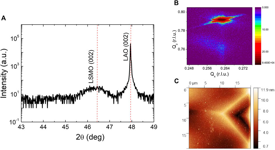
FIGURE 1. (A) XRD pattern of LSMO/LAO thin film showing a smooth and epitaxial growth of ∼ 24 unit cells. This thickness is in close correspondence to that determined by in situ RHEED (Supplementary Figure S1A) and by XRR (Supplementary Figure S1B). The corresponding angles for LSMO (002) and LAO (002) are indicated by the red dotted lines. (B) Reciprocal space map of the (103) Bragg reflection peak of LAO and LSMO shows that the grown film is elongated out of the plane direction to match the lattice parameter of the LAO substrate. (C) AFM image shows structural twin domains of the LAO substrate.

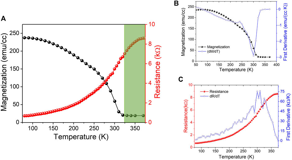
FIGURE 2. (A) Magnetization (black) and resistance (red) vs temperature. The region in white is the ferromagnetic metallic regime, and the green-shaded region is the paramagnetic insulating regime. (B) Zero-field-cooled magnetization vs temperature plot obtained with a running magnetic field of 50 Oe shows that the film follows the Curie–Weiss law exhibiting ferromagnetic behavior up to TC ∼ 325 K, determined by the slope change (dM/dT) with respect to temperature. (C) Zero-field-cooled resistivity vs temperature dependence obtained with a fixed direct current of 1 µA in the van der Pauw configuration, which shows metallic behavior up to TMIT ∼ 325 K, determined by the slope change (dR/dT) with respect to temperature.
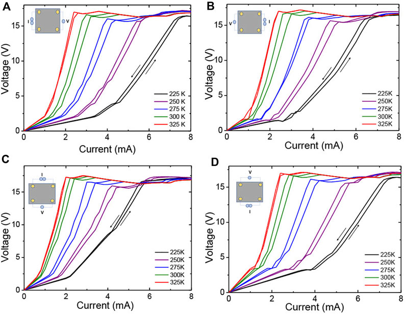
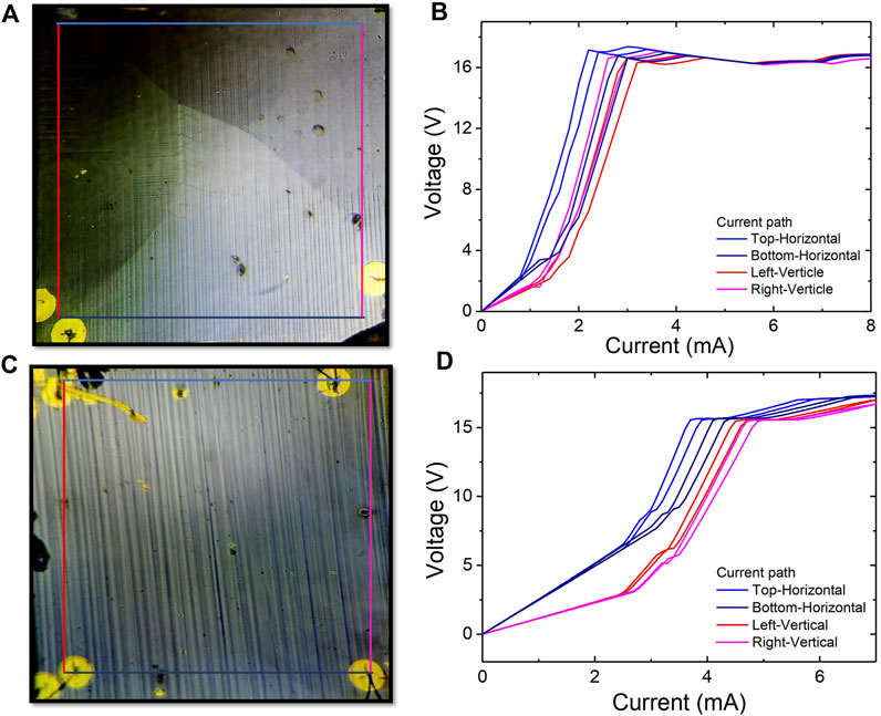
Ti/Au gold contacts were deposited at the four corners of the sample for resistive switching experiments. One pair of contact is chosen at each edge, to source the current, and another pair is used to sense the voltage at the opposite edge. This configuration enables us to probe the entire surface of the film in four different combinations and directions. Voltage (V) vs current (I) sweeps were taken in all directions at different temperatures, as shown in Figure 3. Each graph shows a transition from a linear to non-linear transport across the entire substrate with increasing current. At 225 K, below TMIT, the measured voltage is linear up to 3.25 mA (left-vertical), 2.27 mA (right-vertical), 2 mA (top-horizontal), and 3.62 mA (bottom-horizontal). This is followed by an abrupt change in the slope of the resistance as the current is further increased. This is associated with the transition of the film from a ferromagnetic low-resistance state to a paramagnetic high-resistance state accompanied by a small hysteresis due to Joule heating. A further slope change is observed for higher currents, after which the measured voltage levels off near compliance voltage. The film returns to its initial low-resistance state when the sourced current is ramped to zero, indicative of volatile resistance behavior. Furthermore, as the temperature is increased closer to TMIT, the threshold current for switching decreases, as shown in Figure 3. This is consistent with the associated metal-to-insulator transition, as observed in the R–T measurements (shown in Supplementary Figure S6B). Similarly, the voltage-controlled sweeps (shown in Supplementary Figure S6A) show a rapid increase in current beyond a threshold voltage. Thus, in both measurement types, we identify distinct regimes of changes in resistive states across the entire substrate at each temperature. The corresponding I–V curves measured in all directions show a systematic variation with increasing temperature (Figure 3) (See Supplementary Figure S5 and Supplementary Figure S13). Furthermore, we have carried out similar measurements on different twinned substrates and also on LSMO films of different thicknesses (Supplementary Figures S11, S12). Schematics of the current conduction path along different directions of the films deposited on two distinctly textured LAO substrates are shown in Figures 4A, C. Current vs voltage sweeps in different directions are shown in Figures 4B, D for the two substrates (See Supplementary Figure S9). The optical image of the two substrates shows that the twin domain density, orientation, and homogeneity are different for substrates A and B. The distribution of twin domains influences the magnitude of the current needed to drive the LSMO phase transition, resulting in differences between the two samples and along the different directions as shown in Figures 4A, C. Furthermore, we see that the resistance post-switching and the current at which the voltage (∼ 15 V) levels off are also different for the vertical and horizontal directions. In uniformly terminated substrates, such as in SrTiO3, it is unusual for the dc electrical resistance of LSMO thin films to depend on the measurement direction (Oliveira et al., 2020). In twinned substrates of LAO, however, our findings show that the density, as well as the orientation of the twin domains, yields differences in the resistance when measured along or across the twin boundaries, induced by local changes in strain and electronic properties of the LSMO films.

FIGURE 3. Current-controlled hysteretic resistive switching behavior at different temperatures shown from 225 K to 325 K for (A) left-vertical, (B) right-vertical, (C) top-horizontal, and (D) bottom-horizontal directions. Left (right)-vertical refers to current sourcing in the vertical direction through a pair of left or right contacts. Current sourcing in the horizontal direction using a pair of top or bottom contacts is referred to as top-horizontal or bottom-horizontal. As the temperature increases and approaches TMIT, the current needed for switching to occur decreases establishing the Joule heating origin of the switching.

FIGURE 4. Optical microscopic image of an LSMO thin film grown on a 5 mm × 5 mm (A) inhomogeneously distributed vertical and horizontal twinned domain LAO substrate and (C) homogeneously distributed twinned domains along the vertical direction of the LAO substrate. The corresponding current vs voltage sweeps of (A) and (C) at 300 K are shown in (B) and (D).
4 Discussion
In manganites, non-volatile resistive phase transitions involving structural and stoichiometric changes are well studied (Asamitsu et al., 1997; Kalkert et al., 2011; Jeon et al., 2021). In LSMO, for example, it has been shown that oxygen vacancy-driven resistive phase transitions occur and are accompanied by structural transformations from a perovskite to a brownmillerite phase (Brockman et al., 2014). Volatile resistive switching, on the other hand, utilizes the strong coupling between electronic and magnetic phases (Salev et al., 2021) and does not involve structural phase transitions (See Supplementary Figure S3 and Supplementary Figure S8).
In our case, we determine the resistive switching to be volatile in nature and related to a metal-to-insulator transition in LSMO. We demonstrate electrical control of this transition in Figures 3, 4. Joule heating induces a local increase in temperature, triggering a phase transition when the film temperature locally exceeds TMIT. This is manifested as an abrupt increase in voltage across the entire film and measured by a pair of contacts positioned across different corners of the substrate. The film returns to its original state when the current is ramped down, thus representing a volatile change in the resistance state (Supplementary Figure S10A shows no film degradation up to 100 cycles). By increasing the measurement temperature and bringing it closer to TMIT, the current required for the transition to occur is lowered (Figures 3, 4 and Supplementary Figure S4). Due to the substrate’s morphology involving the random orientation of twin domains, the resistance is expected to depend on whether it is measured across the horizontal or vertical contacts. Rhombohedral wedge-shaped twin domains are frequently observed in the plane of such LAO substrates (shown in Figure 1C and Supplementary Figure S2A). Although these domains are unidirectional, the spacing and angle between the twin boundaries are not equal in all directions. This creates differences in the strain environment, leading to a distribution of ferromagnetic metallic phases with small differences in the oxygen of the MnO6 octahedra, resulting in a complex structure. In such a network, the electrical conductivity is distinctly controlled by the hopping probability of the itinerant d electrons from one Mn site to another, which varies locally due to local differences in the Mn-O-Mn bond angle across or along the twin domains as shown in Figure 3. The accompanying hysteresis results from the lower current needed to maintain the same voltage during retrace. Bare LAO substrates were measured as shown in Supplementary Figure S7; in this case, the resistance is found to be high, and no hysteretic behavior is observed.
5 Conclusion
The current-induced Joule heating-triggered resistive switching that our experiments demonstrate is unlike i) the widely studied Mott insulators that transform to a metallic state from an insulating state by forming a conducting filament parallel to the current flow or ii) LSMO films on well-ordered substrates, such as STO, where the switch from a metallic to an insulating state happens by the formation of a transverse barrier perpendicular to the current flow (Salev et al., 2021). By utilizing a substrate possessing twin domains, we are able to build a complex resistive structure based on the electronic phase transition. The local variations in strain results in a distribution of coexisting ferromagnetic metallic states. Given that each of these phases can transition to a paramagnetic phase at a nominally different threshold current value, this further increases the number of states in the complex structure. Additional tuning of the phase transition temperature is possible by controlling the epitaxial strain through film thickness, which allows control over the switching energy. Both volatile and non-volatile switching can be realized in the same film depending on the proximity of the operating temperature to the transition temperature and on the magnitude of the input stimuli. Contrary to the existing Mott-based memories, no structural transition is associated with the resistive phase transition demonstrated here, making the switching highly stable over a large number of cycles. Our work opens new possibilities for studying such coexisting states using nanoscale probing techniques (Banerjee et al., 2005) as well as for incorporating other transition metal oxides that can provide non-linear strain coupling due to their (pseudo)cubic crystal structure, useful for brain-inspired computing structures. These structures may be exploited in emergent complex learning functionalities ranging from shortest path optimization (Pershin and Di Ventra, 2013) to associative memory (Diaz-Alvarez et al., 2020) or providing a framework for reservoir computing applications.
Data availability statement
The original contributions presented in the study are included in the article/Supplementary Material, further inquiries can be directed to the corresponding authors.
Author contributions
AJ and TB conceived the idea, AJ and AG planned the different experiments including fabrication of the devices, JvR helped with the measurements and data analysis along with LvdZ. The paper was written by AJ and TB with useful input from all authors.
Acknowledgments
The authors would like to thank all members of the Spintronics of Functional Materials group at the University of Groningen, including P. Zhang, S. Chen, and A. Das, for useful scientific discussions. Thin film growth and device fabrication were realized using NanoLab NL facilities. The authors acknowledge technical support from J. Baas, J. G. Holstein, and H. H. de Vries.
Conflict of interest
The authors declare that the research was conducted in the absence of any commercial or financial relationships that could be construed as a potential conflict of interest.
Publisher’s note
All claims expressed in this article are solely those of the authors and do not necessarily represent those of their affiliated organizations, or those of the publisher, the editors and the reviewers. Any product that may be evaluated in this article, or claim that may be made by its manufacturer, is not guaranteed or endorsed by the publisher.
Supplementary material
The Supplementary Material for this article can be found online at: https://www.frontiersin.org/articles/10.3389/fnano.2023.1121492/full#supplementary-material
References
Asamitsu, A., Tomioka, Y., Kuwahara, H., and Tokura, Y. (1997). Current switching of resistive states in magnetoresistive manganites. Nature 388, 50–52. doi:10.1038/40363
Banerjee, T., Haq, E., Siekman, M., Lodder, J., and Jansen, R. (2005). Ballistic hole emission microscopy on metal-semiconductor interfaces. IEEE Trans. Magnetics 41, 2642–2644. doi:10.1109/TMAG.2005.854738
Brockman, J. S., Gao, L., Hughes, B., Rettner, C. T., Samant, M. G., Roche, K. P., et al. (2014). Subnanosecond incubation times for electric-field-induced metallization of a correlated electron oxide. Nat. Nanotechnol. 9, 453–458. doi:10.1038/nnano.2014.71
Burema, A. A., van Rijn, J. J., and Banerjee, T. (2019). Temperature dependence of the magnetization of l a 0.67 s r 0.33 m n o 3 thin films on l a a l o 3. J. Vac. Sci. Technol. A Vac. Surfaces, Films 37, 021103. doi:10.1116/1.5085933
Burema, A., and Banerjee, T. (2021). Temperature-dependent periodicity halving of the in-plane angular magnetoresistance in la0. 67sr0. 33mno3 thin films on laalo3. Appl. Phys. Lett. 119, 011901. doi:10.1063/5.0051629
Diaz-Alvarez, A., Higuchi, R., Li, Q., Shingaya, Y., and Nakayama, T. (2020). Associative routing through neuromorphic nanowire networks. AIP Adv. 10, 025134. doi:10.1063/1.5140579
Dörr, K. (2006). Ferromagnetic manganites: Spin-polarized conduction versus competing interactions. J. Phys. D Appl. Phys. 39, R125–R150. doi:10.1088/0022-3727/39/7/r01
Haeni, J., Theis, C. D., and Schlom, D. G. (2000). Rheed intensity oscillations for the stoichiometric growth of SrTiO3 thin films by reactive molecular beam epitaxy. J. Electroceramics 4, 385–391. doi:10.1023/a:1009947517710
Haghiri-Gosnet, A., and Renard, J. (2003). Cmr manganites: Physics, thin films and devices. J. Phys. D Appl. Phys. 36, R127–R150. doi:10.1088/0022-3727/36/8/201
Hwang, H. Y., Iwasa, Y., Kawasaki, M., Keimer, B., Nagaosa, N., and Tokura, Y. (2012). Emergent phenomena at oxide interfaces. Nat. Mater. 11, 103–113. doi:10.1038/nmat3223
Imada, M., Fujimori, A., and Tokura, Y. (1998). Metal-insulator transitions. Rev. Mod. Phys. 70, 1039–1263. doi:10.1103/revmodphys.70.1039
Izyumskaya, N., Alivov, Y., and Morkoc, H. (2009). Oxides, oxides, and more oxides: High-κ oxides, ferroelectrics, ferromagnetics, and multiferroics. Crit. Rev. Solid State Mater. Sci. 34, 89–179. doi:10.1080/10408430903368401
Jeon, J., Jung, J., and Chow, K. (2021). Electronic phase separation induced non-volatile bi-polar resistive switching in spatially confined manganite microbridges. J. Phys. D Appl. Phys. 54, 315002. doi:10.1088/1361-6463/abfef7
Kalcheim, Y., Camjayi, A., Del Valle, J., Salev, P., Rozenberg, M., and Schuller, I. K. (2020). Non-thermal resistive switching in Mott insulator nanowires. Nat. Commun. 11, 2985–2989. doi:10.1038/s41467-020-16752-1
Kalkert, C., Krisponeit, J.-O., Esseling, M., Lebedev, O. I., Moshnyaga, V., Damaschke, B., et al. (2011). Resistive switching at manganite/manganite interfaces. Appl. Phys. Lett. 99, 132512. doi:10.1063/1.3643425
Kumar, S., Wang, Z., Davila, N., Kumari, N., Norris, K. J., Huang, X., et al. (2017). Physical origins of current and temperature controlled negative differential resistances in NbO2. Nat. Commun. 8, 658. doi:10.1038/s41467-017-00773-4
Liu, X., Li, S., Nandi, S. K., Venkatachalam, D. K., and Elliman, R. G. (2016). Threshold switching and electrical self-oscillation in niobium oxide films. J. Appl. Phys. 120, 124102. doi:10.1063/1.4963288
Oliveira, F., Cipriano, R., da Silva, F., Romão, E., and Dos Santos, C. (2020). Simple analytical method for determining electrical resistivity and sheet resistance using the van der Pauw procedure. Sci. Rep. 10, 16379. doi:10.1038/s41598-020-72097-1
Pershin, Y. V., and Di Ventra, M. (2013). Self-organization and solution of shortest-path optimization problems with memristive networks. Phys. Rev. E 88, 013305. doi:10.1103/physreve.88.013305
Rana, K. G., Yajima, T., Parui, S., Kemper, A. F., Devereaux, T. P., Hikita, Y., et al. (2013). Hot electron transport in a strongly correlated transition-metal oxide. Sci. Rep. 3, 1274. doi:10.1038/srep01274
Roy, S., Autieri, C., Sanyal, B., and Banerjee, T. (2015). Interface control of electronic transport across the magnetic phase transition in srruo3/srtio3 heterointerface. Sci. Rep. 5, 15747. doi:10.1038/srep15747
Salev, P., Fratino, L., Sasaki, D., Berkoun, R., Del Valle, J., Kalcheim, Y., et al. (2021). Transverse barrier formation by electrical triggering of a metal-to-insulator transition. Nat. Commun. 12, 5499. doi:10.1038/s41467-021-25802-1
Stoliar, P., Rozenberg, M., Janod, E., Corraze, B., Tranchant, J., and Cario, L. (2014). Nonthermal and purely electronic resistive switching in a Mott memory. Phys. Rev. B 90, 045146. doi:10.1103/physrevb.90.045146
Štrbík, V., Reiffers, M., Dobročka, E., Šoltỳs, J., Španková, M., and Chromik, Š. (2014). Epitaxial lsmo thin films with correlation of electrical and magnetic properties above 400 k. Appl. Surf. Sci. 312, 212–215. doi:10.1016/j.apsusc.2014.04.045
Sulpizio, J. A., Ilani, S., Irvin, P., and Levy, J. (2014). Nanoscale phenomena in oxide heterostructures. Annu. Rev. Mater. Res. 44, 117–149. doi:10.1146/annurev-matsci-070813-113437
Tokura, Y., and Tomioka, Y. (1999). Colossal magnetoresistive manganites. J. magnetism magnetic Mater. 200, 1–23. doi:10.1016/s0304-8853(99)00352-2
Valmianski, I., Wang, P., Wang, S., Ramirez, J. G., Guénon, S., and Schuller, I. K. (2018). Origin of the current-driven breakdown in vanadium oxides: Thermal versus electronic. Phys. Rev. B 98, 195144. doi:10.1103/physrevb.98.195144
Keywords: volatile memristor, resistive switching, structural twin boundary (TB), neural network, metal to insulator transition (MIT), correlated oxides
Citation: Jaman A, Goossens AS, van Rijn JJL, van der Zee L and Banerjee T (2023) Morphology control of volatile resistive switching in La0.67Sr0.33MnO3 thin films on LaAlO3 (001). Front. Nanotechnol. 5:1121492. doi: 10.3389/fnano.2023.1121492
Received: 11 December 2022; Accepted: 13 February 2023;
Published: 28 February 2023.
Edited by:
Ming Wang, Fudan University, ChinaReviewed by:
Yingfen Wei, Fudan University, ChinaXiaojian Zhu, Chinese Academy of Sciences (CAS), China
Copyright © 2023 Jaman, Goossens, van Rijn, van der Zee and Banerjee. This is an open-access article distributed under the terms of the Creative Commons Attribution License (CC BY). The use, distribution or reproduction in other forums is permitted, provided the original author(s) and the copyright owner(s) are credited and that the original publication in this journal is cited, in accordance with accepted academic practice. No use, distribution or reproduction is permitted which does not comply with these terms.
*Correspondence: A. Jaman, YXptaW51bC5qYW1hbkBydWcubmw=; T. Banerjee, VC5CYW5lcmplZUBydWcubmw=
 A. Jaman
 A. S. Goossens
 J. J. L. van Rijn2
 T. Banerjee